Saumil G. Merchant, Gregory D. Peterson, and Seong G. Kong. Department of Electrical and Computer Engineering. The University of Tennessee. Knoxville, TN ...
Intrinsic Embedded Hardware Evolution of Block-based Neural Networks Saumil G. Merchant, Gregory D. Peterson, and Seong G. Kong Department of Electrical and Computer Engineering The University of Tennessee Knoxville, TN 37996-2100, U.S.A. E-mail: {smerchant,gdp,skong}@utk.edu Abstract - An intrinsic embedded online evolution system has been designed using Block-based neural networks and implemented on Xilinx VirtexIIPro FPGAs. The designed network can dynamically adapt its structure and parameters to input data pattern variations without any FPGA reconfiguration overheads, overcoming a major bottleneck for online evolution systems. With increasing speeds of silicon hardware and availability of faster embedded processors in the near future, a wide spread deployment of these platforms is becoming possible. Keywords: Intrinsic evolution, artificial neural networks, Block-based Neural Networks, Evolvable Hardware
1. Introduction Artificial neural networks (ANNs) have gained a lot of popularity over the last two decades. These networks can effectively model complex non-linear relationships between inputs and outputs and are also widely used to identify patterns in data. In most cases, an ANN is an adaptive system that changes its network structure and parameters based on external or internal information that flows through the network. The network has to be trained using a training dataset to correctly model the input – output mapping. This training is generally a trial and error based method using an objective function to minimize the error with multiple iterations. With offline training algorithms, an optimal network once found is frozen and deployed in production systems. But dynamics of many real world problems demand an online training and adaptation of the network to adjust to the changing input data patterns. The inherent parallelism in these networks is best exploited with custom digital hardware designs which can achieve much higher training as well as recall speeds, compared to the equivalent software implementations. But the lack of a general solution to determine the network structure and parameters and the required regular updates in the trial and error based training process, make these networks difficult to implement in static digital hardware like the ASICs (Application Specific Integrated Circuits). Higher routing requirements for popular fully connected multilayer perceptron models of artificial neural networks incur expensive redesigning, re-routing and fabrication penalties with addition of even a single neuron in one of the hidden layers. To gain the advantage of higher speedups associated with hardware implementations and the flexibility of
software implementations, FPGAs seem to be a more suitable choice. FPGA implementations can offer significant speedups over software implementations with the flexibility of runtime hardware reconfiguration. Many researchers have taken this route relying on full / partial FPGA reconfiguration capability to reuse the hardware for different applications on the designed artificial neural network [1-6]. But this again is a favorable approach for a statically frozen network. For a dynamic evolution system the FPGA reconfiguration overheads, which typically run in the order of a few milli-seconds would take away, any speedups advantages obtained in hardware implementation. This paper presents an intrinsic embedded hardware design of block-based neural networks (BbNNs) [7-10] that can be evolved dynamically to find the optimal network structure and parameters without requiring multiple FPGA reconfigurations. Intrinsic hardware evolution is an online evolution paradigm where the evolutionary algorithm is directly changing the hardware as opposed to an extrinsic model in which evolutionary algorithm is wrapped around a software model of the system [11]. This design has been targeted for Xilinx® VirtexIIPro™ (XC2VP30) FPGA. The design was implemented on Amirix AP130 platform housing the Xilinx FPGA chip.
2. Block-based Neural Networks Block-based neural networks are grid-based network structures of interconnected block-based neurons, the basic processing elements of the network. Each neuron block can have up to 3 inputs, 3 outputs and 9 synaptic weights and biases depending on the internal configuration determined by the network structure. The outputs are a function of weighted summation of inputs and a bias. The activation function on the output nodes can be linear (e.g., ‘purelin’) or a nonlinear function (e.g., ‘tangent sigmoid’). Depending on the internal configuration of the block, we can have a 2input / 2-output block, 1-input / 3-output block and 3-input / 1-output block. The structure and synaptic weights and biases of a network are encoded as genes in a BbNN chromosome for genetic evolution. A random population of these networks is genetically evolved using genetic operators like selection, crossover and mutation, over many generations to find a best candidate network that meets the target fitness [7-10, 12]. Although BbNN blocks structures can support a feedback connection with the bottom node
being an input we have initially restricted our hardware implementation to only feedforward networks for simplicity in hardware design and because many interesting applications can be successfully implemented as feedforward networks.
3. Hardware Design of BbNN Numerous successful FPGA implementations of artificial neural networks have been reported in the literature. Extensive use of multiplier and accumulator units in ANNs have directed many researchers to encode real data in bit streams to implement multipliers in a serial fashion avoiding area expensive direct implementations and compromising on computational speed. Real values have been encoded using pulse-streams [13], digital bit serial stochastic techniques [2, 14], delta encoded binary sequences [15], or vector based approach [16] to improve real estate efficiency for multipliers and accumulators. Some direct implementations have also been reported that use full or partial FPGA reconfigurations to reuse the reconfigurable fabric [1, 3-6, 17]. A review of the FPGA implementations by Zhu and Sutton [18], identifies general issues faced for hardware implementations of ANNs like the reconfiguration time overheads, activation function implementation and data precision used.
3.1. Reconfiguration Time Overheads Typical FPGA reconfiguration times being in order of a few milli seconds can pose a significant overhead when multiple FPGA reconfigurations are required during genetic evolution. Good performance can only be achieved if reconfiguration time is small compared to the computational time. The reconfigurable logic should be used q times before a reconfiguration cycle. This is a breakeven point beyond which density enhancement is no longer profitable. In [19], q is given by the equation: q = r /( s − 1) where r is the time (in cycles) taken to reconfigure the FPGA and s is the total computation time after each reconfiguration. In our implementation of BbNN the FPGA is initialized to support a maximum desired network size that can fit on the chip. Individual SBbNs can be selectively turned on/off in the network as needed using only the required subset of the network initialized in FPGA for fitness evaluation of a particular BbNN candidate. Thus, for example a 5x10 network in the FPGA can be used for any subsets like 2×10, 3×4, 5×9 etc. This eliminates any need for FPGA reconfiguration.
3.2. Activation Function Implementation Direct implementations of nonlinear activation functions can be expensive in terms of resource costs. A more practical approach would be to use a piecewise-linear approximation of the non-linear activation function [6] or a lookup table approach [5] which essentially pre-stores the output values of the activation function in memory. Advantages of using a LUT based approach is simplicity in
design, flexibility to use any activation function depending on the application at hand without hardware redesign and a 2 clock cycle lookup, but is expensive in terms of FPGA area. In our implementation of BbNN we have opted for LUT based approach using the available block RAMs in the Xilinx VirtexIIPro FPGA chip. Since these BRAMs are hardcoded in the chip they do not use a lot of reconfigurable FPGA fabric. Also, due to saturating nature of the typical activation functions we use a 12 bits × 16 bits (8 Kbytes) LUT, instead of 16 bits × 16 bits (128 Kbytes) LUT and hardcode the higher (or lower) out of range lookups to the positive saturation (or negative saturation) value of the activation function.
3.3. Data Representation and Precision A floating-point representation of data (weights, biases, inputs and outputs) in a neural network may still be impractical to implement on FPGAs despite the current advances in FPGA technology [20]. Thus fixed point implementations are preferred over floating point implementations as these can use regular integer multipliers and adders to compute the results. The choice of data precision is guided by the implementation cost in terms of area, simplicity of design, speed and power consumption. Higher precision will lead to less quantization error in the final implementation, while lower precision will produce more compact and faster designs consuming less power. A judicious choice needs to be made depending on the application at hand and available FPGA resources. Our current implementation uses 8.8 fixed point representations for the real values. A higher resolution network of 16.16 fixed point representations is currently being designed. The choice of data precision used would also be driven by the size of the activation function lookup table. Higher precision would require a much bigger table.
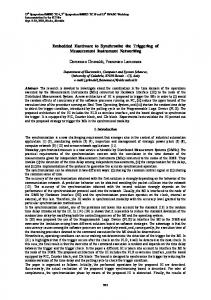
3.4. Design of Smart Block-Based Neurons For an online evolution system we need a block design that can be software configured to emulate any of the internal configurations of a general BbNN block. Based on this requirement a smart BbNN block (SBbN) was designed that can emulate any BbNN block configuration depending on the structure gene inputted to the FPGA. Figure 1 illustrates the idea. The bold synaptic connections are the active connections for the particular BbNN configuration emulated at the time as shown in Figure 1b. These blocks can also be selectively turned off/on using gray mode configuration in which the block is inactive and simply passes the inputs to outputs. Connecting these SBbNs in a grid like fashion creates a completely software configurable BbNN. Figure 2 shows internal logical diagram. The dataflow through the network has been implemented as a control structure inspired by Petri-net model architecture. Every block in the network ‘fires’ when it has valid input tokens on all of its input nodes, consuming all the input tokens and generating output tokens for every output node which are fed to inputs of the neighboring blocks.
and configure the network structure and weights of individual SBbNs and configure the activation function lookup table.
4.2. Processing Speeds
Figure 1 (a) SBbN model (b) Emulated 2/2 configuration
Figure 2 SBbN Internal Logical Diagram
The BbNN design gets its clock signal from OPB and hence runs at the 40 MHz, the clock rate of OPB. Currently this is one of the limiting factors on processing speed of our design as our synthesis results show peak clock frequency of 80 MHz. Once the input data, structure and synaptic weights are loaded to the FPGA each block takes 10 OPB clock cycles to compute the outputs on all of its output nodes. So considering a worst case scenario, a 3×3 BbNN would need 9 block computations to compute the final output, which is 90 OPB clock cycles or 2.25 µs. Depending on the internal configuration of a block, each block computation can involve up to a maximum of 8 connections (e.g., a 2/2 configuration). Thus, each block has a peak connection per second speed of 32 MCPS per block for a 16 bit data width. With generally more than one block computing at a time, depending on the network structure the peak CPS would be (n computing blocks)×(32 MCPS/block) processing speed. For example, a 16 block network could achieve up to 512 MCPS. In practice, typical BbNN execution cycles would achieve less than this bound depending on the specific network configuration.
4. Implementation
4.3. A Case Study
The BbNN structure described above was designed in VHDL and implemented as a programmable system-onchip (PSoC) on a Xilinx VirtexIIPro FPGA (XC2VP30) housed on an Amirix AP130 development board. The FPGA has two on-chip PowerPC 405 processors, 30,816 logic cells, 2448 KBits of on-chip BRAMs, 136 multiplier blocks (18×18) and 8 digital clock managers. This design of SBbNs is much smaller in footprint occupying only 396 logic slices, 4 BRAMs and one 18×18 multiplier; which is about 1% of logic slice usage on XC2VP30 FPGA. An earlier brute force library based approach occupied 327-582 slices depending on the internal configuration of the block [17]. Using these blocks a 3×3 BbNN grid occupies 4570 slice registers, 12 BRAMs and twenty-one 18×18 multipliers; which is about 16% of logic slice usage on XC2VP30 FPGA. Amirix provides a baseline platform along with the development board which is the default PSoC configured on the FPGA. The designed network has been added to this platform using Xilinx Embedded Development Kit toolset. It communicates with PowerPC 405 as a slave on the OPB (On-chip Peripheral Bus). On-chip PowerPC processors can run a software environment such as Timesys Linux or just a boot monitor program like PPCBoot which can be used to control the associated hardware resources.
The developed design was tested for an ‘Exclusive OR’ pattern classification problem. The GA evolution was coded in C running on on-chip PowerPC processor using the software interface to communicate with the in network designed on the FPGA for fitness evolution.
4.1. Software Interface BbNN hardware can be configured via a software interface available in C and C++, running on a PowerPC on the FPGA chip. The interface is designed to control and configure the BbNN in FPGA. It has functions to initialize
5. Conclusion An efficient intrinsic embedded online evolution system using BbNN was successfully designed. This network can be genetically evolved to find a candidate network that meets the desired target fitness. It is a completely software configurable general BbNN and can be used as a platform for further explorations. Being an embedded design it can be deployed in many real world scenarios like mobile robot navigation systems [7], pattern recognition [8], signal prediction applications [9] and ECG classification applications [10]. Currently our design gives 32 MCPS/block processing speeds when connected to the OPB bus running at 40 MHz. We are investigating possibilities of directly connecting the designed network to PLB bus running at 80 MHz, which would at least double our processing speed to 64MCPS/block. The GA evolution code currently runs on on-chip PowerPC processor on the VirtexIIpro FPGA, running at 300 MHz giving a throughput of 600+ MIPS. On the next generation Virtex4 FPGAs from Xilinx the supported CLK frequency has been increased to 450MHz with a throughput of 700+ MIPS. It is one of the faster processors available for programmable SoC applications on FPGAs. Following the trends in increasing processing
capabilities and decreasing feature sizes of silicon based systems as predicted by Moore’s law and availability of faster and higher capacity FPGA chips makes this approach more compelling over time. Achronix Semiconductor Corporation has already announced production of over 1 GHz FPGA chips by the end of this calendar year. Being more noise tolerant in extreme environments and economic feasibility of design and production make FPGAs a more favorable choice for a wide range of embedded applications. Also, the designed network being a digital system has higher noise immunity over some other analog approaches of ANN implementations. Many interesting research directions emanate from this base capability. We are currently investigating real-time scheduling techniques to reuse a network in real-time using temporal slicing where in the deployed network processes input data giving output results and immediately switches back to a training mode adapting the network to changing data patterns, again switching back to deployed mode on receiving newer data for processing. In fact, two separate networks could be used where one network continuously adapts and evolves using the real-time data and the other processes the data outputting the results. This reduces the downtime for retraining the systems. Also, taking advantage of the high speed serial connection busses on these FPGAs we can connect multiple FPGAs to develop a parallel distributed processing system. We are also investigating faster more efficient algorithms that can adapt the network in real-time and converge to desired target fitness.
6. Acknowledgment This work was supported in part by the National Science Foundation under grant Nos. ECS-0319002 and CCF-0311500.
7. References [1] C. E. Cox and W. E. Blanz, "GANGLION-a fast fieldprogrammable gate array implementation of a connectionist classifier," IEEE Journal of Solid-State Circuits, vol. 27, pp. 288-299, 1992. [2] G. P. K. Economou, et al, "FPGA implementation of artificial neural networks: an application on medical expert systems," Proc. 4th Intl. Conference on Microelectronics for Neural Networks and Fuzzy Systems., 1994. [3] J. G. Eldredge and B. L. Hutchings, "Density enhancement of a neural network using FPGAs and run-time reconfiguration," Proc. IEEE Workshop on FPGAs for Custom Computing Machines, 1994. [4] R. Gadea, et al, "Artificial neural network implementation on a single FPGA of a pipelined online backpropagation," 2000. [5] M. Krips, T. Lammert, and A. Kummert, "FPGA implementation of a neural network for a real-time hand tracking system," Proc. 1st IEEE Intl. Workshop on Electronic Design, Test and Applications, 2002.
[6] M. Porrmann, U. Witkowski, H. Kalte, and U. Ruckert, "Implementation of artificial neural networks on a reconfigurable hardware accelerator," Proc. 10th Euromicro Workshop Parallel, Distributed and Network-based Processing, 2002. [7] S. W. Moon and S. G. Kong, "Block-based neural networks," IEEE Transactions on Neural Networks, vol. 12, pp. 307-317, 2001. [8] S. W. Moon and S. G. Kong, "Pattern recognition with block-based neural networks," Proc. Intl. Joint Conference on Neural Networks (IJCNN-2002), 2002. [9] S. G. Kong, "Time series prediction with evolvable block-based neural networks," Proc. Intl. Joint Conference on Neural Networks (IJCNN-2004), 2004. [10] W. Jiang, S. G. Kong, and G. D. Peterson, "ECG Signal Classification using Block-based Neural Networks," Proc. Intl. Joint Conference on Neural Networks (IJCNN-2005), 2005. [11] H. DeGaris, "Evolvable Hardware : Principles and Practice”http://www.cs.usu.edu/~degaris/papers/CAC M-E-Hard.html, 1997. [12] S. Merchant, G. D. Peterson, S. K. Park, and S. G. Kong, "FPGA Implementation of Evolvable Blockbased Neural Networks," Proc. IEEE Congress on Evolutionary Computation, Vancouver, Canada, 2006. [13] P. Lysaght, et al, "Artificial Neural Network Implementation on a Fine-Grained FPGA," Proc. 4th Intl. Workshop on Field-Programmable Logic and Applications, Prague, Czech Republic, 1994. [14] M. van Daalen, et al, "Emergent activation functions from a stochastic bit-stream neuron," Electronics Letters, vol. 30, pp. 331-333, 1994. [15] V. Salapura, "Neural networks using bit stream arithmetic: a space efficient implementation," IEEE Intl. Symposium on Circuits and Systems. ISCAS '94., 1994. [16] S. A. Guccione and M. J. Gonzalez, "Neural network implementation using reconfigurable architectures," in Selected papers from the Oxford 1993 Intl. workshop on field programmable logic and applications on More FPGAs. Oxford, United Kingdom, 1994. [17] S. Kothandaraman, "Implementation of Block-based Neural Networks on Reconfigurable Computing Platforms," in ECE Dept, MS. Knoxville: University of Tennessee, 2004. [18] J. Zhu and P. Sutton, "FPGA Implementation of Neural Networks - A Survey of a Decade of Progress," 13th Intl. Conference on Field-Programmable Logic and Applications Lisbon, Portugal, 2003. [19] G. Steve and J. G. Mario, "Classification and Performance of Reconfigurable Architectures," in Proc. 5th Intl. Workshop on Field-Programmable Logic and Applications: Springer-Verlag, 1995. [20] K. Nichols, M. and S. A. Moussa, "Feasibility of Floating-Point Arithmetic in FPGA based Artificial Neural Networks," Proc. 15th Intl. Conference on Computer Applications in Industry and Engineering, San Diego, California, 2002.