ISAST Transactions on Electronics and Signal Processing, No. 2, Vol. 3, 2008 Brian Daniels and Ronan Farrell: Rigorous Stability Criterion for Digital Phase Locked Loops
1
Rigorous Stability Criterion for Digital Phase Locked Loops Brian Daniels and Ronan Farrell
Abstract—This paper proposes a rigorous stability criterion for an arbitrary order digital phase locked loop (DPLL), with a charge pump phase frequency detector (CP-PFD) component. Stability boundaries for such systems are determined using piecewise linear methods to model the nonlinear nature of the CP-PFD component block. The model calculates the control voltage, after a predetermined number of input reference signal sampling periods, to a small initial voltage offset. This paper, in particular, takes an in-depth look at the second order system. The second order stability boundaries, as defined by the proposed technique, are compared to that of existing linear theory stability boundaries, and display a significant improvement. The applicability of the proposed technique to higher order systems, using a numerically iterative solution, is presented. Finally the proposed methodology is used to determine the stability boundary of a third order system and thus the component values for a stable system. Using these component values the response of the DPLL to an initial control voltage offset is simulated using a circuit level simulation. Index Terms—High Order, Phase Locked Loop, Piecewise Linear, Stability.
I.
INTRODUCTION
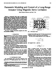
The Digital Phase Locked Loop (DPLL) is a versatile component block widely used in electronics for operations such as frequency synthesis and clock data recovery. The DPLL system considered in this paper consists of a bang bang phase frequency detector (PFD), a charge pump (CP), a voltage controlled oscillator (VCO), and a low pass loop filter (LF), with a structure as shown in fig. 1. Manuscript received March 25, 2008. Research presented in this paper was funded by a Centre for Telecommunications Value-Chain Research (SFI 03/CE3/I405) by Science Foundation Ireland under the National Development Plan, and by the Enterprise Ireland Commercialisation Fund. The authors gratefully acknowledge this support. B. Daniels is with the Institute of Microelectronics and Wireless Systems, National University of Ireland Maynooth, Maynooth, County Kildare, Ireland, (e-mail:
[email protected]) R. Farrell is with the Centre for Telecommunications Value-Chain Research, National University of Ireland Maynooth, Maynooth, County Kildare, Ireland, (e-mail:
[email protected])
FR
PFD
CP IP LF VC
VCO
FV
FV/N
÷N Fig. 1.
DPLL Loop Block Diagram
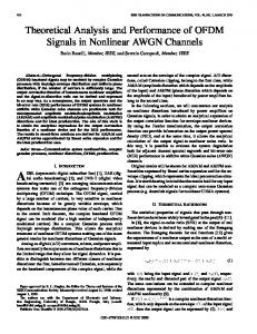
The DPLL loop uses a local oscillator reference signal to generate a robust signal at the output of the VCO. The phase of the reference and feedback signals are compared by the PFD and any difference is represented as a current on the charge pump output, IP. This error drives the VCO output signal towards that of the reference, and thus drives the loop towards lock. The most basic type of PLL, a first order PLL, has no loop filter and thus it is globally stable. But it produces large frequency jitter or phase noise on the output signal that is intolerable for most applications. It is normal practice to include a loop filter to reduce this jitter. Ideally the higher the order of filter the lower the phase noise on the output signal. However the inclusion of a loop filter introduces stability concerns that now need to be considered during the design process [1]. Because of these stability issues it is considered risky to design DPLL systems of order greater than third. Thus the second and third order DPLLs are the most common PLLs designed today. The DPLL loop filter structure for the third order loop is shown in fig. 2. In the case of a second order DPLL the capacitor C3 is removed. This paper aims to provide an alternative methodology that enables the design of high order systems by accurately determining their stability boundaries. To achieve this, a number of issues need to be considered; first the nonlinearity of the DPLL loop; and second the complexity of the higher order DPLL linear equations.
ISAST Transactions on Electronics and Signal Processing, No. 2, Vol. 3, 2008 Brian Daniels and Ronan Farrell: Rigorous Stability Criterion for Digital Phase Locked Loops
2 IP
VC R2 C3 C2
Fig. 2.
Third Order DPLL filter Structure
The nonlinearities of the DPLL system exist in the CPPFD and the VCO component blocks. The VCO can be assumed linear if the DPLL system operates away from the saturation regions of the VCO. The non-linearity in the PFD is due to quantization-like effects at the output of the PFD. This non-linearity is inherent to the operation of the loop and cannot be ignored if an accurate model is required. Due to this inherent non-linearity, linearization, which ignores this quantization, is not entirely accurate. Thus it is generally the case that empirical design and simulation are used concurrently to ensure the correct behaviour. This design methodology is outlined graphically in the flow chart of fig. 3. Traditionally the designer starts with a linear model and then applies rule of thumb or empirical simulation design techniques to redefine the system parameters.
loop bandwidth, from a fast locking wide bandwidth loop when the PLL is out of lock, to a low noise narrow bandwidth loop when loop lock is detected. Similarly dualloops achieve fast lock and low noise using two feedback loops simultaneously, one loop has a wide bandwidth to allow fast lock and the second loop has narrow bandwidth for a low noise signal output. This paper proposes a novel arbitrary-order stability criterion using piecewise linear methods to accurately model the inherent non-linear nature of the CP-PFD. The stability criterion is applicable to all orders of the DPLL system described earlier, with model equations given for each order of system from second through to fifth. In the case of the second order system a closed form solution of the stability criterion is determined, whereas numerical iteration is used to solve the equations for higher orders. The stability boundary is found for the second and third order DPLLs, and compared to the results from existing published linear models. In the next section traditional DPLL design techniques are considered. In section III the proposed piecewise linear model is introduced. Section IV takes, as an example, a more detailed look at the second order system and determines the stability boundary for this system. This boundary is compared to that of the linear model defined boundary of Gardner [1]. In section V the piecewise linear model’s applicability to high orders is considered. Finally in section VI conclusions are presented.
Linear Model Initial System Parameters
Rules of Thumb Redefined System Parameters
Empirical Design Simulation Response Bad Good
End Fig. 3.
Traditional Design Method
The alternative to the above, are nonlinear stability methods, however these are found to be unwieldy and further complicate the design of an already complex system. For this reason non-linear methods have only rarely been applied to the design of PLL systems [2-5]. There are other means of stabilising the DPLL by using advanced architecture techniques, for example gear-shifting [6,7], or aided acquisition dual-loops [8,9]. Gear-shifting varies the
TRADITIONAL DESIGN TECHNIQUES
II.
Start
Traditionally the DPLL is linearised by replacing the PFD component with a subtractor component block in the analysis. This can be justified if the time-varying nature of the PFD is overlooked. This is a reasonable approximation when considering the PLL to be close to lock. In this situation it’s key state variable, the VCO control voltage, changes by only a small amount on each cycle of the reference signal. This is known as the continuous time approximation and is valid when the loop bandwidth is small relative to the reference frequency, or more specifically no greater than 1/10th of the reference frequency [1]. This assumes that the detailed behaviour of the loop within each cycle is not important and only the average behaviour over many cycles is important. By applying an averaged analysis, the time-varying operation can be bypassed and linear analysis can be applied. The DPLL system of fig. 1 is approximated by the linear system block diagram as shown in fig. 4. PD
φR
+
φe -
KP
F(s)
VC
VCO KV s
1 N
Fig. 4.
Linear PLL (LPLL) system
φV
ISAST Transactions on Electronics and Signal Processing, No. 2, Vol. 3, 2008 Brian Daniels and Ronan Farrell: Rigorous Stability Criterion for Digital Phase Locked Loops
The feedback frequency divider is used in frequency synthesis to produce an output signal frequency that is some multiple of the reference signal, N times FR in fig. 1. The inclusion of a feedback divider scales FV by N. In our analysis the divider introduces a scaling factor, however in this paper the feedback divide ratio is chosen to be equal to 1 for clarity. The transfer function of the LPLL system of fig. 4 is then given by:
KV I P F ( s ) H CL ( s ) = 2π s + KV I P F ( s )
(1)
where IP is the charge pump current gain, KV is the VCO gain and F(s) is the loop filter transfer function. Using (1), Gardner [1] identifies the stability boundary for the second order PLL system to be:
K′ =
1
π § π · ¨1 + ¸ ω Rτ 2 © ω Rτ 2 ¹
(2)
A plot of the stability boundary from equation (2) for a defined filter time constant τ2, and a range of reference frequencies (ωR radians/second) are shown in fig. 5. -8
1
x 10
0.9 0.8
Unstable Region
0.7
K’
0.6 0.5 0.4 0.3 0.2
Stable Region
0.1 0
Fig. 5.
0
0.5
1
1.5
ωRτ2
2
2.5
3
3.5
x 10
-4
Second order Gardner Stability Boundary
For the 3rd order system Gardner offers a similar stability boundary as defined by (3).
K'
V0 then the system trajectory is diverging and is therefore unstable; If |Vm| < V0 then the trajectory is converging and is stable. The calculation of φe(t) and VC(t) depends on the filter’s charge approximated difference equations. For the second order system φe(t) and VC(t) are determined using the set of difference equations (4) and (5). For higher order PLLs additional state variables need to be considered, specifically the charge on each additional filter capacitor. However if VC(t) reaches a stable equilibrium then the filter capacitor state variables have also reached the equilibrium. Therefore when considering the stability of a high order system, we need only monitor φe(t) and VC(t). I T VC ( tn +1 ) = VC ( tn ) − P B (4) C2
(
(
φe (tn +1 ) = φe (tn ) + 2π T ( FR − FFR ) − KV ³ VC dt
))
VC
T
-IPR2 −
t(n+1)
TC
Fig. 7.
φe ( tn ) T 2π
(6)
where φe(tn) is the phase error at time tn. The coast time period is calculated as TC = TB - T. Once the time periods are calculated, VC can be determined using (4). To solve equation (5) an estimate of the integral of VC is required. For the second order DPLL, the loop filter is first order, and therefore the integration corresponds to a linear ramp and can be expressed as:
³ VC dt = TVC ( tn ) − TB I P R2 −
TB
One Period of VC for 2nd Order DPLL
I PTB C2
TB2 I P 2C2
(7)
As discussed earlier high order DPLLs have high order differential terms in their system equations, thus finding a closed form solution equivalent to the second order equations above becomes a difficult task. The solution suggested here is to approximate the high order system equations using charge approximation as presented in [13]. This approach converts a set of parallel integral equations into a set of linear difference equations. It considers the charge on each capacitor rather than the voltage at each node, making the assumption that the average current Iavg through a capacitor during the period Δt, which is unknown, is equal to the current at time t, I(t), as in fig. 8. IP
(5)
where FFR is the VCO free running frequency, and KV is the VCO gain, T is the reference signal time period, and TB is defined here as the boost time of the CP-PFD or the length of time during each period T where the CP-PFD pumps a non zero current into the loop filter. To further clarify consider one time period, T, of the loop. In this time period the DPLL operates in the coast state, where no current is output from the CP-PFD, for a period of time defined here as TC, and in boost state for a period of TB, as in fig. 7. TB is calculated as in equation (6).
t(n)
TB =
Average Current Approximation
t
Fig. 8.
Δt
t+1
Assumption that current at time t is equal to the average current during Δt
Utilising charge approximation, the complexity is reduced making it possible to derive closed form solutions to higher order DPLL systems. This can be justified for high frequency systems as a large FR will result in a small period T, making the approximation more accurate. For clarity consider the third order system before charge approximation is applied as in equation (8).
VC (t + 1) = I P R2 − C3 R2
dVc 1 C + I p dt − 3 Vc (t ) ³ dt C2 C2
(8)
This equation is complicated by differential and integral terms, as the order increases the equivalent VC solution becomes increasingly complex. Using charge approximation this equation can be rewritten as those given in equations (A1), (A3) and (A4) from appendix A. While these
ISAST Transactions on Electronics and Signal Processing, No. 2, Vol. 3, 2008 Brian Daniels and Ronan Farrell: Rigorous Stability Criterion for Digital Phase Locked Loops
5
equations may appear to be more expansive they do not have any differential terms. The benefit is more significant for 5th and 6th order systems as they cannot be solved in closed form without making such an approximation. The error introduced due to this approximation is bounded and tends to zero as the time interval Δt tends to zero, as shown in fig. 9(a) and fig. 9(b). For large reference frequencies or a small initial VC offset Δt, the error due to the charge approximation is minimal. The relevant charge approximated difference equations for a number of filters of increasing order are given in appendix A.
Ideal Response
Δt
Fig. 9.
Error
Zero Order Hold Approx
Small Δt Reduced Error
(a) Zero order hold approximation with large Δt, (b) smaller Δt smaller Error
This model is a significant improvement over existing methods in that it is more accurate and results in simpler system equations, due to a combination of the piecewise linear method and the charge approximation. Using the methodology described in this section it is possible to determine the stability boundaries for any DPLL system by numerically iterating the charge approximated system equations given in appendix A, for a small initial VC offset, by looking at the system trajectory over a short period of time as shown in fig. 6. This is achievable for any order of DPLL system using numerical iteration; however it is possible to determine a closed form stability criterion for the second order system by extending the methodology described here. This is considered in the next section. IV.
SECOND ORDER PIECEWISE LINEAR MODEL
In this section a more detailed consideration of the piecewise linear model, in the case of the second order DPLL, is given. This approach determines the second order DPLL control voltage after m periods of the reference signal, Vm, as defined in fig. 6. The solution of Vm is used to define a closed form solution of the DPLL stability boundary for the second order system. To determine Vm two things need to be considered: first, when all parameters are known, any nth sample of the control voltage Vn needs to be calculated in closed form; and second the number of samples m needs to be calculated where Vm is the control voltage at the first zero crossing of the phase error as shown in fig. 6. These two requirements are considered in the following two subsections.
1) Calculation of Vn The second order system, described by equations (4), and (5) can be reduced to the pair of summations given in (9) and (10), where V0 is an initial positive VC offset, the initial φe offset is zero, and φe is always negative as in fig. 6. I T n −1 VC (n ) = V0 + P ¦ φe ( j ) (9) 2π C2 j =0 j −1
φe ( j ) = −2π KV T ¦ (1 − KV TI P R2 )
j − k −1
k =0
VC ( k )
(10)
Equations (9) and (10) may be combined to give: K I T 2 n −1 j −1 j − k −1 Vn = V0 − V P ¦¦ (1 − KV I P R2T ) VC ( k ) (11) C2 j =0 k =0 where Vn is equivalent to VC(n) and is an exact calculation of the control voltage after n samples. The double summation in equation (11) can be solved by either numerical iteration, or by solving a closed form simplification. This closed form solution is considered later in subsection 3. The control voltage at the zero crossing, Vm will not correspond exactly with Vn, as the last sample n will not fall exactly on the phase error zero crossing, but will cross that line by some value d, as shown in fig. 10. If samples n-1 and n are both known then it is possible to calculate the value of Vm by using a linear interpolation (12). (0,0)
Φe
n-1
n d
VC
Fig. 10. State Space Samples
Vm = Vy − φ y
Vx − Vy
φx + φ y
(12)
where (Vx, φx) and (Vy, φy) are the co-ordinates of the samples n and n-1 respectively in fig. 10. However (12) is not used in this model as the error introduced in the calculation of Vm is minimal and reduces as the reference frequency is increased. 2) Calculation of number of samples m To calculate the number of samples m it is necessary to return to the linear approximation model and use the linear error transfer function:
H e (s) =
C2 s 2 C2 s 2 + KV I P R2C2 s + KV I P
(13)
Using linear theory to determine m does not reduce the accuracy of this technique, as we only require an approximate value of m and then round it up to the next
ISAST Transactions on Electronics and Signal Processing, No. 2, Vol. 3, 2008 Brian Daniels and Ronan Farrell: Rigorous Stability Criterion for Digital Phase Locked Loops
6
integer. To determine the phase error zero crossings the frequency step response of (13) is calculated and the inverse Laplace taken as shown in (14) and equated to zero.
§ 2πΔ · L−1 ¨ 2 F H e ( s ) ¸ = 0 © s ¹
(14)
where ΔF is the frequency step size. Solving (14) gives an equation of the form A(t)Sin(X(t))=0, which is zero when X(t)=0,π,2π,3π,… The first zero crossing after t = 0 occurs when X(t)=π. Solving this gives equation (15), the time of the first zero crossing.
tm =
2π ( KV I P (4 − KV I P R C2 )) / C2 2 2
(15)
The number of samples in one half cycle of the state space trajectory, (the solid arc of the system trajectory in fig. 6) is estimated as: ª º 2π FR m = «ªtm FR + 1»º = « + 1» (16) «« ( KV I P (4 − KV I P R22C2 )) / C2 »» 3) Closed Form Solution of Vm The value of Vm, the control voltage at the first zero crossing of the phase error, can be found using equations (11) and (16) and numerical iteration. However it is also possible to solve equation (11) in closed form, as shown below.
Pin = 100
V0 + Vm % V0
(19)
If the pull-in percentage is negative, the system is unstable otherwise the system is stable. Combining (18) and (19) the stability criterion can be simplified to:
2 + AΛ1 + A2 Λ 2 + A3 Λ 3 + A4 Λ 4 > 0
(20)
This is independent of the initial VCO control voltage offset V0. As would be expected, the initial condition does not have any effect on the stability boundary. Equating (20) to zero gives the stability boundary of the system and can be compared to the traditional stability boundary of [1]. In fig. 11 the stability boundaries of the proposed second order technique are determined for a pull-in rate of 1%, 20% and 40% and are shown along with Gardner’s linear boundary [1] and a stability boundary defined by a number of circuit level simulations. The accuracy of the circuit level simulation has been verified using other published behavioural and event driven DPLL models [14-16]. 0.5 0.45
Unstable Region
0.4
Piecewise Linear Boundaries
Linear Boundary
0.35 0.3
Kτ2
ª º « » «1 + A ( Λ1 ) » « 2 » «+ A ( Λ 2 ) » » Vm = V0 « + A3 ( Λ 3 ) « » «# » « ªmº » ·» « «« 2 »» § « + A ¨¨ Λ ª m º ¸¸ » «¬ © «« 2 »» ¹ »¼
An important system performance criterion is the pull-in rate. Using the system trajectory, as in fig. 6 and Vm, the system pull-in rate can be determined for an initial VCO control voltage offset V0.
40%
0.25
20%
0.2 0.15
1% Circuit level Simulation
0.1
(17)
where A= -KVIP/(FR2C2) and Λ1 up to Λªm/2º are a set of parameters defined as equations (B1-B5) from appendix B. Since parameter |A| is always