4.1.1 The Element . . . . . . . . . . . . 8. 4.1.2 The .... an array of processing elements (PE) that contain sub-word processing units with only very few ... type (PE-level). In order to validate a MAML-code we use a MAML Document Type Definition (DTD) ...... instructions (e.g., multiply and add, y = âi ai · bi) with ...
Friedrich-Alexander-Universität Erlangen-Nürnberg
MAML - An Architecture Description Language for Modeling and Simulation of Processor Array Architectures Part I Alexey Kupriyanov, Frank Hannig, Dmitrij Kissler, Rainer Schaffer ∗, J¨urgen Teich Department of Computer Science 12 Hardware-Software-Co-Design University of Erlangen-Nuremberg Am Weichselgarten 3 D-91058 Erlangen, Germany Co-Design-Report 03-2006
March 14, 2006 ∗
Dresden University of Technology, Department of Electrical Engineering and Information Technology, Institute of Circuits and Systems
1
Contents 1 Abstract
3
2 Introduction
3
3 Related Work
4
4 Characterization of Regular Architectures 4.1 Array-Level Architecture Specification . . . . . . . . . . . 4.1.1 The Element . . . . . . . 4.1.2 The Element . . . . . . . . . . . 4.1.3 The Interconnect Domain Element 4.1.4 The Subelement 4.1.5 The Subelement . . . . . . . . . 4.1.6 The Subelement . . . . . 4.1.7 The PE Class Domain Element 4.2 PE-Level Architecture Specification . . . . . . . . . . . . 4.2.1 The Element . . . . . . . . . . . . . 4.2.2 The Element . . . . . . . . . . . . 4.2.3 The Element . . . . . . . . . . . 4.2.4 The Element . . . . . . 4.2.5 The Element . . . . . . . . . . . . . 4.2.6 The Element . . . . . . . . . . . . 4.2.7 The Element . . . . . . . . . . 4.2.8 The Element . . . . . . . . . . . . . . 4.3 Simulation . . . . . . . . . . . . . . . . . . . . . . . . . .
. . . . . . . . . . . . . . . . .
. . . . . . . . . . . . . . . . . .
. . . . . . . . . . . . . . . . . .
. . . . . . . . . . . . . . . . . .
. . . . . . . . . . . . . . . . . .
6 8 8 13 13 20 21 21 21 22 23 25 26 26 28 30 35 38 39
5 WPPA Design Flow in Scopes of ArchitectureComposer Framework 40 6 Conclusions and Future Work
42
A MAML Document Type Definition
45
B Example: WPPA Description in MAML
52
References
63
2
1 Abstract In this report, we introduce an architecture description language (ADL) for the systematic characterization, modeling, simulation and evaluation of massively parallel reconfigurable processor architectures that are designed for special purpose applications from the domain of embedded systems. Numerous ADLs have been developed to describe different capabilities of architectural modeling and analysis. But, unfortunately, there is no ADL so far which could describe massively parallel processor arrays. The ADL proposed in this report is being developed to characterize such architectures. The architectural description of the processor system is supposed to be done according to two abstraction levels of massively parallel reconfigurable processor architectures. Architectural parameters of processor elements are characterized on the (lower) processor element level and the interaction between processor elements (i.e., interconnect topology, positioning of each PE, etc.) is described on the (higher) processor array level. Key features, grammar, and technical innovations of the proposed ADL are covered in this report.
2 Introduction Today, the steady technological progress in integration densities and modern nanotechnology will allow implementations of hundreds of 32-bit microprocessors and more on a single die (System-on-a-Chip technology). Furthermore, the functionality of the microprocessors increases continuously, e.g., by parallel processing of data with low accuracy (8 bit or 16 bit) within each microprocessor. Due to these advances, massively parallel data processing has become possible in portable and other embedded systems. These devices have to handle increasingly computationalintensive algorithms like video processing (H.264) or other digital signal processing tasks (3G), but on the other hand they are subject to strict limitations in their cost and/or power budget. These kind of applications can only be efficiently realized if design tools are able to identify the inherent parallelism of a given algorithm and if they are able to map it into correctly functional, reliable, and highly optimized systems with respect to cost, performance, and energy/power consumption. But, technical analysts foresee the dilemma of not being able to fully exploit next generation hardware complexity because of a lack of mapping tools. Hence, parallelization techniques and compilers will be of utmost importance in order to map computational-intensive algorithms efficiently to these processor arrays. At all times, there was the exigence (demands at speed, size, cost, power, etc.) to develop dedicated massively parallel hardware in terms of ASICs (Application Specific Integrated Circuits). For instance, let us consider the area of image processing, where a cost-benefit analysis is of crucial importance: On a given input image, sequences of millions of similar operations on adjacent picture elements (pixel) (e.g.,
3
Architectural Research I/O
I/O
WPPE
WPPE
WPPE
WPPE
WPPE
WPPE
WPPE
WPPE
WPPE
WPPE
WPPE
WPPE
WPPE
WPPE
I/O
WPPE
I/O
Co-Exploration
Modeling, Simulation, Emulation
I/O
Retargetable Mapping Methodology
I/O
Algorithms
I/O
WPPE
I/O
Figure 1: Co-design flow. 2- or 3-dimensional filter algorithms, edge detection, Hough transformation) have to be computed within splits of a second. The use of general purpose parallel computers like MIMD or SIMD multiprocessor machines is not reasonable because such systems are too large and expensive. Such machines are also of no use in the context of mobile environments where additional criteria such as energy consumption, weight and geometrical dimensions exclude solutions with (several) general purpose processors. In order to avoid huge area and thus cost overheads of general purpose computers, the architecture of choice is problem- or domain-specific. The main problem is that the development of a new architecture requires also suitable compilers and mapping tools, respectively. Parameterizable architecture and compiler co-design will therefore be a key step in the development of such embedded systems in the future (see Figure 1). The main challenges are on the one hand side the extraction of common properties of regular designs independent of hardware and software, respectively. On the other side, the analysis of program transformations and architecture parameters is of great importance in order to achieve highly efficient and optimized systems. Concepts of retargetable compilers are needed for array-like architectures. One major milestone here is to study and understand the correlation and matching of architectural parameters with the parameters of program transformations as part of such compilers.
3 Related Work Many architecture description languages have been developed in the field of retargetable compilation. In the following, we list only some of the most significant ADLs. For instance, the hardware description language nML [FVF95] permits concise, hierarchical processor descriptions in a behavioral style. nML is used in the CBC/SIGH/SIM framework [Fau95] and the CHESS system [GVL+ 96]. The machine description language LISA [PHM00] is the basis for a retargetable compiled simulator approach developed at RWTH Aachen, Germany. The project focuses on fast simulator generation for already existing architectures to be modeled in LISA. Current works in the domain of multi-core system simulation [KPBT06, ACL+ 06] enable a co-simulation of multiple processor cores with busses and peripheral modules which are described in SystemC. At the ACES laboratory of the University of
4
California, Irvine, the architecture description language EXPRESSION [HGK+ 99] has been developed. From an EXPRESSION description of an architecture, the retargetable compiler Express and a cycle-accurate simulator can be automatically generated. The Trimaran system [Tri] has been designed to generate efficient VLIW code. It is based on a fixed basic architecture (HPL-PD) being parameterizable in the number of registers, the number of functional units, and operation latencies. Parameters of the machine are specified in the description language HMDES. MIMOLA [LM98] is one of RT-level ADLs. It was developed at the University of Kiel, Germany. Originally, it targeted at micro-architecture modeling and design. Some of register transfer level (RTL) hardware description languages were also used for modeling and simulation of processor architectures, i.e. UDL/I [Aka96] was developed at Kyushu University in Japan. It describes the input to the COACH ASIP design automation system. A target specific compiler can be generated based on the instruction set extracted from the UDL/I description. The instruction set simulator can also be generated to supplement the cycle accurate RT-level simulator. ISDL is one of Instruction Set Description Languages. It was developed at MIT and is used by the Aviv compiler [Han99] and the associated assembler. It was also used by the simulator generation system GENSIM [HRD99]. The target architectures for ISDL are VLIW ASIPs. Maril is an ADL used by the retargetable compiler Marion [BHE91]. It contains both instruction set information as well as coarse-grained structural information. The target architectures for Maril are RISC style processors only. There is no distinction between instruction and operation in Maril. TDL stands for target description language. It has been developed at Saarland University in Germany. The language is used in a retargetable post-pass assembly-based code optimization system called PROPAN [Kae00]. Another architecture description language is PRMDL [TPE01]. PRMDL stands for Philips Research Machine Description Language. The target architectures for PRMDL are clustered VLIW architectures. Finally, we refer to the Machine Markup Language (MAML) which has been developed in the BUILDABONG project [FTTW01]. MAML is used for the efficient architecture/compiler co-generation of ASIPs and VLIW processor architectures. For a more complete ADL’s summary we point out to the surveys in [QM02], [THG+ 99], and [MD05]. All these ADLs have in common that they have been developed for the design of single processor architectures such as ASIPs which might contain VLIW execution. But, to the best of our knowledge, there exists no ADL which covers the architectural aspects of massively parallel processor arrays. Of course, one could use hardware description languages such as Verilog or VHDL but these languages are too low level and offer only insufficient possibilities to describe behavioral aspects.
5
Programmable Interconnection I/O
WPPE
WPPE
WPPE
WPPE
ip0 ip1 ip2 ip3 Input Registers/FIFOs
I/O
WPPE
I/O
I/O
WPPE
I/O
WPPE
WPPE
WPPE
WPPE
i1
i2
i3
regI
regGP
WPPE
rPorts
WPPE
General Purpose Regs i0
WPPE
WPPE
WPPE
WPPE
WPPE
WPPE
WPPE
WPPE
WPPE
WPPE
WPPE
WPPE
WPPE
WPPE
WPPE
WPPE
mux
Instruction Memory
I/O
WPPE
I/O
WPPE
mux
ALU type1
pc
WPPE
WPPE
I/O
WPPE
WPPE
I/O
WPPE
f1 wPorts
regFlags
BUnit
I/O
I/O
demux
f0
WPPE
Output Registers
o0
o1 regO
r0 r1 r2 r3 r4 r5 r6 r7 r8 r9 r10 r11 r12 r13 r14 r15
Instruction Decoder
op0 op1
I/O
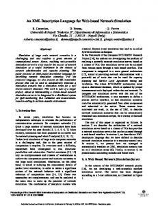
Figure 2: Example of a WPPA with parameterizable processing elements (WPPEs). A WPPE consists of a processing unit which contains a set of functional units. Some functional units allow to compute sub-words in sub-word units in parallel. The processing unit is connected to input and output registers. A small data memory exists to temporary store computational results. An instruction sequencer exists as part of the control path which executes a set of control instructions from a local tiny program memory.
4 Characterization of Regular Architectures As an example of massively parallel reconfigurable architectures we introduce a new class of them - weakly-programmable arrays (WPPA). Such architectures consist of an array of processing elements (PE) that contain sub-word processing units with only very few memory and a regular interconnect structure. In order to efficiently implement a certain algorithm, each PE may implement only a certain function range. Also, the instruction set is limited and may be configured at compile-time or even dynamically at run-time. The PEs are called weakly-programmable because the control overhead of each PE is optimized and kept small. An example of such an architecture is shown in Figure 2. The massive parallelism might be expressed by different types of parallelism: (1) several parallel working weakly-programmable processing elements (WPPEs), (2) functional and software pipelining, (3) multiple functional units within one WPPE, and finally (4) sub-word parallelism (SWP) within the WPPEs. WPPAs can be seen as a compromise between programmability and speciality by exploiting architectures realizing the full synergy of programmable processor elements and dedicated processing units. Since design time and cost are critical aspects during the design of processor architectures it is important to provide efficient modeling and simulation techniques
6
maml
name
ProcessorArray Array-Level
PEClass ... PEClass PE-Level
Figure 3: Root element . in order to evaluate architecture prototypes without actually designing them. In the scope of the methodology presented here, we are looking for a flexible reconfigurable architecture in order to find out trade-offs between different architecture peculiarities for a given set of applications. Therefore, a formal description of architecture properties is of great importance. In order to allow the specification of massively parallel processor architectures we use the MAchine Markup Language (MAML) [FTTW01] and provide extensions that are needed for modeling WPPAs. MAML is based on XML notation and is used for describing architecture parameters required by possible mapping methods such as partitioning, scheduling, functional unit and register allocation. Moreover, the parameters extracted from a MAML architectural description can be used for interactive visualization and simulation of the given processor architecture. The four main constraints of well-formed XML documents were followed in order to define MAML due to the XML standard: (i) there is exactly one root element, (ii) every start tag has a matching end tag, (iii) no tag overlaps another tag, and (iv) all elements and attributes must obey the naming constraints. A MAML document has one root element with an attribute name, specifying the file name of the architecture. Example 4.1 Root element of MAML. ...
The architectural description of an entire WPPA can be subdivided into two main abstraction levels, the array-level describing parameters such as the topology of the interconnection, number and location of processor and I/O-ports, etc., and the PElevel describing the internal structure of each WPPE’s type the WPPA may be composed of. The general structure of a MAML specification is shown in Figure 3. The MAML elements and attributes are presented by the ellipses and rectangles, respectively. The elements in the MAML are strictly ordered from left to right. First, the
7
ProcessorArray
PElements
name version
PEInterconnectWrapper
name rows columns
ICDomain ... ICDomain name selection
ClassDomain ... ClassDomain name peclass selection
Figure 4: The element. processor array architecture should be described on the array-level and only then follows the specification of the internal structure of each WPPE’s type (PE-level). In order to validate a MAML-code we use a MAML Document Type Definition (DTD) which is completely listed in Appendix A.
4.1 Array-Level Architecture Specification The array-level properties of a WPPA are described in the body of a special MAML element . This element specifies the parameters of the whole WPPA in general, i.e., the name of the WPPA, the interconnect topology, the number and types of WPPEs, etc. For instance, if the WPPA has a mesh structure of PEs the size of the WPPA must be given in terms of the number of columns and rows. The interconnect between processor array cells is one of the very important parameters of a WPPA. 4.1.1 The Element The structure of the element is shown in Figure 4. This element contains the attributes name and version specifying the name of the processor array architecture and its version, respectively. It also contains a set of subelements: • • • •
8
c1
c1
c2
c2
c2
c2
c3
c3
c3
c3
c1
c1
c1
c1
c2
c2
c2
c2
c3
c3
c3
c3
c1
c1
c1
c1
c2
c2
c2
c2
c3
c3
c3
c3
c1
c1
c1
c1
c2
c2
c2
c2
c3
c3
c3
c3
c1
c1
ICDomain d1
ICDomain d2
ICDomain d3
ICDomain d4
ICDomain D
Figure 5: Interconnect Domains and Class Domains representation. The multiple definition of the subelements and is admissible. (stands for Processor Elements) defines the number of PEs in the whole processor array, gives the referring name for them. The number of elements is specified as two-dimensional array with fixed number of rows (rows attribute) and columns (cols attribute). The number of rows multiplied by the number of columns is not necessarily the total number of processors within the array. Since as discussed above, the grid serves only as basis in order to place different types of processors, memories, and I/O-elements. Furthermore, each grid point does not necessarily correspond to one element because the size of the elements could be different. Here, size in terms of physical area is rather subordinate but the logical size in terms of connectors. specifies an interconnect wrapper (IW) which wraps each processor element of the processor array. All interconnect wrappers are directly connected to each other via their ingoing and outgoing signal ports on each side. Also, an interconnect wrapper describes the ingoing and outgoing signal ports of a processor element inside it, thus providing the interconnection between the PEs in the whole processor array. A schematic view of it is shown in Figure 7 (the explanations follow in Section 4.1.3). Although each processor element with possibly different internal architecture is placed inside of the interconnect wrapper, the parameters of the IWs are common for the entire processor array. Therefore, these parameters are specified in the array-level of the MAML description. (Interconnect Domain) specifies the set or domain of the processor elements with the same interconnect topology. The PEs here are either the subsets of the set of PEs defined by the element or another domain. Recursive definition is not allowed.
9
specifies the set or domain of the processor elements with the same architectural structure (PE Class). The PEs here are either the subsets of the set of PEs defined by the element or another domain. Recursive definition is not allowed. In Figure 5, an example of interconnect and class domains representation of a processor array architecture is presented. Four interconnect and three class domains are shown. The interconnect domain d1 contains the PEs of class c1. The interconnect domain d2 contains the PEs of class c2. The interconnect domain d3 contains the PEs of class c3. And finally, the interconnect domain d4 contains PEs of class c1 again. The interconnect topology for the PEs in the interconnect domain d2 is shown in Figure 10. In the following, the processor array definition for the example in Figure 5 is listed. The complete MAML-code for this example is listed in Appendix B. Example 4.2 Processor array definition.
10
11
12
4.1.2 The Element The attributes: • name • rows • columns defines the set of PEs that are used for constructing the whole processor array. The name attribute names the set of PEs. The rows and columns attributes define the 2D size of the array of PEs. Example 4.3 2D size definition of the processor array.
The set pe with 48 PEs (4 × 12 array) is defined. Each element can be referred by the name of the set and the 2D indices. In the example above, we can refer each PE as follows: pe[1,1]..pe[4,12]. 4.1.3 The Interconnect Domain Element The interconnect domain is used to specify the interconnect topology for a set of PEs. There are a lot of different interconnect topologies (i.e., see Figure 6) but the selection one of them is always a trade-off. The supported topology classes are: 1. Nearest neighbor topologies like line horizontal, vertical lines (grid) (Figure 6(a)), honeycomb (Figure 6(b,c)),
13
(a)
(d) I/O
I/O
I/O
I/O
I/O
I/O
I/O
I/O
(b)
(c)
(e)
(f)
Figure 6: Examples of Interconnect topologies: (a) grid, (b,c) honeycomb, (d) bus, (e) crossbar, and (f) fat tree. 2. Bus (i.e., PACT array [BEM+ 03], see Figure 6(d)), 3. Crossbar (Figure 6(e)), 4. Tree (binary, k-ary, Fat in Figure 6(f)), and 5. Torus. In order to be able to model and specify any possible interconnect topology within MAML, a PE interconnect wrapper (IW) concept is introduced (see Figure 7(a)). An interconnect wrapper describes the ingoing and outgoing signal ports of a processor element. Each interconnect wrapper has a constant number of inputs and outputs on each of its side which are connected to the inputs and output of neighbor IW instances. An interconnect wrapper is represented as a rectangle around a PE and consists of the input and output ports on the northern, eastern, southern, and western side of it. However, the input ports and the output ports on the opposite sides of an IW (i.e., northern inputs and southern outputs) must have equal bitwidths and the number of them must be the same. Introduction of this condition proves the correct interconnection between neighbor IW instances. The condition can be completely satisfied by the introduction of directed interconnect channels. Each directed interconnect channel represents the pair of one input and one output port on the opposite sides of the interconnect wrapper with a certain common bitwidth. The direction of the channel is determined by the position of the output port. For example, if we consider a pair
14
N in
(a) 0 0
N out
1
2
...
0
1
2
... 0
Interconnect Wrapper P in
1
W out
0
1
2
1
E in
3 ...
2
2
PE
.. .
.. .
0
0
1
0
W in
1
2
1
3 ...
E out
P out
2
.. .
2
.. .
Eastward interconnect channel
0
1
2
...
0
1
...
S in
S out (b)
2
Interconnect Adjacency Matrix
j
N
out
E out
i
S out
P in
W out
·
N in
· ·
E in
·
S
·
in
·
·
·
cij
·
·
·
·
·
·
W in
· ·
P out
· ·
cij ←
1, if ∃ a possible connection between input and output ports, 0, otherwise;
Figure 7: Interconnect Wrapper (a) and Interconnect Adjacency Matrix (b). 15
of northern input and southern output IW ports, then the direction of corresponding interconnect channel is southward. The interconnection between all interconnect wrappers of the processor array is correct if and only if each IW has equivalent directed interconnect channels. The number of input ports is represented by the N in , E in , S in ,and W in for each side respectively. The same holds for the output ports: N out , E out , S out , and W out . The numbering of the ports is done as shown in Figure 7(a). The indices of the pair of IW ports which belong to the certain interconnect channel are the same and equal to the index of this interconnect channel. The consecutive numbering of interconnect channels is done in the directions from left to right and from top to bottom. A PE is placed inside of the interconnect wrapper. The input ports P in are shown on the top edge and the output ports P out are shown on the bottom edge of the PE. The configuration of an IW is specified by the so-called Interconnect Adjacency Matrix (IAM) (see Figure 7(b)). By the configuration of an IW, we mean the definition of the mapping of the possible connections between the ports of an interconnect wrapper and a processor element. Therefore, the particular ports of an IW should be considered instead of interconnect channels (the pair of ports). The rows of IAM represent the input ports of an IW, except the last few rows (dependent on the number of the PEs output ports), which represent the output ports of the PE. The columns represent the output ports of an IW, except the last few columns (dependent on the number of the PEs input ports), which represent the input ports of the PE. The matrix contains the values cij , which are equal to ”1” if there exists a possible connection between input and output ports, and equal to ”0” otherwise. The last rows and columns of IAM represent the port mapping between PE and IW ports. The interconnection of PE ports is not allowed, however the interconnection of IW ports is possible. The positions of input PE ports are interchanged with the positions of the output PE ports in the IAM. This allows to avoid the configuration of such incorrect connections as a connection between IW input and PE output or a connection between PE input and IW output. � 1, if ∃ a possible connection between input and output ports, cij ← 0, otherwise; In the most complex case, the IW is a configurable full crossbar switched matrix, but in practice, in the most cases, it is less complex since it is a compromise between routing flexibility and cost. The IW is defined by the element. It contains the specifications of the interconnect channels (index and bitwidth) in each direction and the definition of maximal number of PE input and output ports. An example of an IAM for the interconnect topology in Figure 10 is shown in the code on page 10 (see the interconnect domain d2). The structure of the element is depicted in Figure 8. The element contains the attributes name, selection, and the following subelements:
16
ICDomain
name selection
Interconnect ElementsPolytopeRange ... ElementsPolytopeRange ElementAt ... ElementsDomain ... ElementsDomain
Figure 8: The element. • • • • specifies the domain of the processor elements with the same interconnect topology. The processor elements within an interconnect domain are the subsets of PEs defined by the element. The selection of the processor elements which should be included into interconnect domain is done by usage of the following elements: , , and . These elements define a range of PEs in the shape of a given polytope, the particular PE with given coordinates (row, column), or the subset of PEs specified by the name of another domain. Recursive definition is not allowed. The name attribute gives the name to the interconnect domain. The selection attribute specifies how different subsets of PEs defined by the elements , , or should be compound in resulting selection of PEs in the entire interconnect domain. The selection attribute allows one of the following values: addition (this is a default value if the selection attribute is not specified), subtraction, or intersection. This values stand for the composition of resulting selection by the addition (union), subtraction or intersection of PE-subsets, respectively. For example, we have a 3 × 3 processor array and want to define a ring-shaped interconnect domain which contains all PEs except one in the center, as shown in Figure 9(a). In this case, the interconnect domain should be specified with an attribute selection set to subtraction and two PE subsets. The first subset should select all PEs by a polytope definition (detailed explanation of this element follows in Section 4.1.4). The second subset which contains only one processor element PE[2,2] defined by (see Section 4.1.5) is subtracted from the first
17
(a)
(b)
RingDomain IW
IW
PE[1,1]
IW PE[1,2]
IW
...
PE[1,3]
IW PE[2,1]
IW
PE[2,2]
IW PE[3,1]
PE[2,3]
IW PE[3,2]
PE[3,3]
Figure 9: Example of an interconnect domain definition using the selection attribute. subset. This results in required ring-shaped interconnect domain. The corresponding MAML-code is shown in Figure 9(b). The subelement specifies the interconnect network topology. The attribute type defines the type of the interconnect. The value of the type is either "static" or "dynamic" specifying the reconfigurability of the interconnect. If the interconnect of certain PE or of the whole domain is reconfigurable, the special interconnect control registers will be added to the interconnect wrappers in order to drive the process of interconnect reconfiguration. The details concerning dynamic reconfiguration of massively parallel processor architectures will be covered in Part II of this report in the near future. The subelement defines the IAM of the interconnect wrapper for the PEs which belong to the current domain. The matrix is described row by row using the elements , , , , and with the attributes idx and row, specifying the rows of the matrix (rows with all zeros can be skipped). These elements represent the input ports of an IW and output ports of the PE. The value of idx defines the index of the corresponding interconnect channel which contains the specified IW input port. The numbering order of the interconnect channels is explained on page 16. Figure 10 shows the interconnect wrappers with four input and four output ports on each of its edges. All of them contain PEs with four input and four output ports. Here, the interconnect topology represents the interconnect domain d2 in Figure 5. The code for this interconnect topology is listed bellow. Example 4.4 Definition of the interconnect topology.
18
PE
PE
wrapper
PE
PE
wrapper
wrapper
PE
wrapper
PE
PE
wrapper
PE
PE
PE
wrapper
wrapper
PE
wrapper
PE
wrapper
wrapper
wrapper
PE
wrapper
PE
PE
wrapper
wrapper
PE
wrapper
wrapper
Figure 10: The interconnect topology of the PEs from interconnect domain d2 in Figure 5.
19
4.1.4 The Subelement j= i
j
3 c2
2 1
j=4
c2
4
c2
c2
1
2
c2
c2
c2
c2
D1 c2 c2 3
4
5
c3
c3
c3
D2 c3 6
7
j=1 8
i
DomainD1:
�� � � � � � � � � � � 4 1 0 � � x 0 x 1 0 i i i 6 −1 ∧ 0 −1 + = = ∈ Z2 | y 0 y 0 1 j j j 0 −1 1
DomainD2:
1 1 0 � � � � � � � � � � � � � � 0 5 −1 0 x x i i i 2 0 2 6 ∧ = + = ∈Z | 1 0 1 1 y y j j j 0 2 0 0 −1
Figure 11: Polytope domains representation. The subelement is used to define a subset of PEs that are grouped together in order to organize one domain. The set of PEs is defined by the points of an integer lattice defined as follows: � � �� � � � � � � � � i i i x x 2 = ∈Z | =L· +m ∧ A· 6b j j j y y � � � � x x A· 6 b describes a polytope which is affinely transformed by L · + m. y y An example of this concept is shown in Fig. 11. The processor array contains two
20
domains of processor elements: domain D1 has a triangular shape and domain D2 is a set of PEs placed in shape of square. The MAML-code listed below describes the polytope domain D2 in Figure 11. Example 4.5 Characterization of Polytope domain.
If matrix L and vector m are not specified, they are assumed to be unity, zero, respectively. The default values for matrix L is thus the identity matrix and for vector m the vector of zeroes. 4.1.5 The Subelement The subelement is used to select one single PE by the index of its row and column in the processor array where it is placed. contains two corresponding attributes: row and column. 4.1.6 The Subelement The subelement selects the subset of PEs already specified in another domain. The instance attribute specifies the name of this domain instance. The recursive definition is not allowed here. 4.1.7 The PE Class Domain Element specifies the set of the processor elements with the same architectural structure (PE class). The processor elements within a class domain are the subsets of PEs defined by the element. The selection of the processor elements that should be included into the PE class domain is done in the same manner as in the definition of the interconnect domain (see Section 4.1.3). The structure of the element is depicted in Figure 12. contains the attributes name, peclass, and selection. The name attribute gives a name to the domain. The peclass attribute specifies the
21
name ClassDomain peclass selection
ElementsPolytopeRange ... ElementsPolytopeRange ElementAt ... ElementsDomain ... ElementsDomain
Figure 12: The element. class name of the PE architecture for all PEs in this domain. This name should match the name of any PE class specified in the PE-level section of a MAML description. Classes of a PE architecture are described in Section 4.2. The subelements , , and are the same as for the element (see Section 4.1.3).
4.2 PE-Level Architecture Specification A schematic view of a possible WPPE is depicted in Figure 2. The processor element consists of three register files: input registers regI, output registers regO, and general purpose registers regGP. As a special register, it contains also a program counter pc and a set of registers-flags form the register bank regFlags. Consequently, the registers from regI are given the names i plus the index from 0 to 3, as we have four input registers. The registers which belong to regO can be referred to with the names o0, o1 in the same manner. The registers of regGP are referred to by r0..r15. The flag-registers are named f0, f1. Input and output registers are connected to the input and output ports: {ip0, ip1, ip2, ip3} and {op0, op1}, respectively. Reading from and writing to the registers of any register bank is established through the read- and write ports (rPort, wPort). A WPPE can have one or several functional units (FUs) of the same or different ALU types which can increase the performance of a WPPE by enabling parallel computing by the execution of VLIW instructions. FUs with a wide word width might be also configured to provide sub-word parallelism. SWP allows the parallel execution of equal instructions with low data word width (e.g., four additions with 16 bit data) on functional units with high data word width (e.g., a 64 P bit adder). Also the execution of complex instructions (e.g., multiply and add, y = i ai · bi ) with multiply data input (e.g., 4 data pairs with 16 bit word width) and single data output (e.g., 1 data with 64 bit word width) is possible. Consequently, the type of SWP (operation and number of sub-words) has to be given in the description for each FU in order to enable a modeling of SWP instructions. Mostly those sub-words which are packed together in full
22
length words have to be rearranged for the next calculation. Therefore, additional instructions are needed which are called packing instructions. The packing instructions can be added to the instruction set of already given FUs or they can be implemented as an instruction set of dedicated packing FU. As the sub-words are stored in words of full length, and the rearranging will be done within FUs, there is no additional characterization of those registers which are involved in the SWP needed. An instruction decoder decodes the processor instructions stored in the instruction memory and drives the multiplexors and demultiplexors which select registers and register banks for the source and target (result) operands of FUs. In order to provide a complete design flow, starting from the architecture specification and finishing by the compiler generation the results of compilation must be represented in binary code, so that we can put this binary code as a stimuli entry data for WPPE architecture simulation. In order to handle this, the MAML description uses an instruction image binary coding. The internal structure of a PE is described in the PE-level architecture specification section of MAML. The architectural properties of PEs are defined by the so called PE-classes. The properties of one class can be instanced as well on the one PE as on the set of PEs. PE-classes can extend or implement another already earlier defined PE-classes, thus providing larger MAML-code efficiency. PE-classes are defined by the element. 4.2.1 The Element The element specifies the internal architecture of the PE or set of the processor elements (PE-class) within a massively parallel processor architecture. It covers such architectural issues as shown in the following: • Characterization of I/O ports (bitwidth, input/output/biderectional, control path or data path, etc.), • Internal resources (internal read/write ports, FUs, busses, etc.), • Storage elements (data or control registers, local memories, instruction memory, FIFOs, feed-back FIFOs, register files, etc.) • Resource mapping (interconnection of the ports with internal elements), • Instructions (instruction coding, functionality, SWP), and • Functional units (resource usage, pipeline, etc.). The structure of the element is shown in Figure 13. MAML allows the specification of multiple PE-classes, whereas one PE-class can extend or implement another earlier defined PE-class. This feature enables the inheritance among
23
name PEClass implements
IOPorts
StorageElements Resources
Opnames Resmap
Units
Operations
Figure 13: The element. PE-classes in the architecture specification. The element contains the following attributes: • name • implements The name attribute names the PE-class. The implements attribute provides the name of another PE-class of all subelements and parameters which are copied to the current PE-class. The further description of any subelement in the body of this class will overwrite the appropriate subelement. The implements attribute can be omitted which would mean that the PE-class is supposed to be constructed from scratch. Example 4.6 PE-classes inheritance in MAML. ... ... ... ... ... ... ...
The element contains the following subelements:
24
• • • • • • • They are described in the following sections in detail. 4.2.2 The Element The section specifies the input and output ports of the processor element. The ports are connected to inputs and outputs of the interconnect wrapper. The element specifies a certain I/O port. It contains the following attributes: • name • bitwidth • direction • type The attributes define the name, bitwidth, direction (in, our, or inout), and type (data or ctrl) of a PE port, respectively. Example 4.7 Definition of PE I/O ports.
Data ports --> name="ip0" bitwidth="32" direction="in" type="data"/> name="ip1" bitwidth="32" direction="in" type="data"/> name="op0" bitwidth="32" direction="out" type="data"/> name="op1" bitwidth="32" direction="out" type="data"/> Control ports --> name="ic0" bitwidth="1" direction="in" type="ctrl"/> name="ic1" bitwidth="1" direction="in" type="ctrl"/> name="oc0" bitwidth="1" direction="out" type="ctrl"/> name="oc1" bitwidth="1" direction="out" type="ctrl"/>
25
StorageElements
Register
FBFIFO
RegisterBank
SpRegister
LocalMemory InstructionMemory
FBFIFOBank PortMapping
FIFO FIFOBank
Bank
Element
Figure 14: The element. 4.2.3 The Element The attributes: • name • num The description of communication components (i.e., read/write ports, busses,...) of the internal architecture of PE is provided by the element. The name attribute names the communication resource, and the num attribute sets the quantity of it. In case of a bus resource, the num attribute sets the width of the bus. Example 4.8 Definition of PE internal resources.
4.2.4 The Element The element specifies the storage components (register files, separate registers, local memory, instruction memory, FIFOs) of the internal architecture of PE. The general structure of it is shown in Figure 14. The element contains the following subelements:
26
FIFO
...
mux
Figure 15: A schematic view of a Feed-back-FIFO. • or • or • or • • • • The element defines a register by its name, bitwidth and type (data or control) parameters which are set by the attributes name, bitwidth, and type, respectively. The specifies the register bank (the set of the registers) by the definition of the attributes name, number (number of the registers in the register bank), bitwidth, type, and namespace. The name attribute gives a name to the register bank, whereas the namespace attribute defines a name space (a name without index) for all registers in the register bank. In order to distinguish between ordinary registers and FIFOs, the elements , , , and are defined. Each of them has the same attribute set as for the elements and only the additional attribute depth specifies the depth of the FIFO. The and elements are used to describe feed-back-FIFOs which could be useful for data reuse. A schematic view of a feed-back-FIFO is shown in Figure 15. provides the specification of the special registers in a certain register or FIFO bank. The instruction memory is separated from the local memory by the use of element InstructionMemory with the memory size (number of memory words) and
27
bitwidth as attributes. The local memory is defined by the element LocalMemory in the same manner as definition of instruction memory. The element declares the direct connections between the registers or FIFOs and I/O ports, defined in the element (see Section 4.2.2). Thus, the routing between the internal storage elements of different processor elements through the interconnect wrapper ports is established. Example 4.9 Characterization of PE storage elements within MAML.
4.2.5 The Element The Element describes the resource mapping [Kr¨u02]. This element assigns the read/write ports to the register banks, connects the functional units to the register banks through the buses, and defines the pipeline stages.
28
The assignment of read/write ports is set by the case bank of get rport and case bank of get wport subelements of the corresponding elements and . The attribute bank defines a name of the register or FIFO bank, and rport or wport attributes select read or write ports. The dependencies specified here are extracted by the entry of a keyword get rport or get wport in the appropriate subelement of the element (see Section 4.2.7). The interconnection of functional units to the register banks or FIFOs through the buses is described in the element . The dependencies specified here are extracted by the entry of a keyword get bus in the appropriate subelement of the element. The element allocates the pipeline stages. The description of this element is optional. If there is no specification of this element in a MAML description, then the pipeline stages are allocated as shown in the following example. Example 4.10 Resource mapping in MAML.
29
... ... output function in C ... ... ...
Figure 16: Description of the function(s) of an operation 4.2.6 The Element All operations and binary image coding for them are listed by the Opnames element. The operation name is specified by the attribute name and the operation image binary coding is set by the code attribute. Example 4.11 All operations of the architecture should be listed. ...
30
... ... ...
The functional description for each operation () is given as sub-element functionDescription here also. The general overview of the functional description is given in Figure 16. The functional description regards the use of SWP. Therefore, the description of the input and output data scheme (, ) is needed in the output function as well. The number of input and output data, the number of sub-words in a data word, and the type of the sub-words are described in the elements and . The element describes the output function for each sub-word or for a set of sub-words. The syntax of the element and its sub-elements is given in the DTD style as follows:
• : Description of all operations • : Description of one operation – name: Name of the operation. The name has to be unique.
31
– code: Machine code for the operation. The code has to be unique. • : Description of the instruction functionality. This includes the input and output data scheme (inputData, outputData) and the output function (outputFunction). Dependent on the input output scheme, several descriptions for a SWP instruction can be given. • : Description of one or more input data words. If all input data words are equal, only one word (word) has to be described. Otherwise, each word has to be described separately. – namespace: Name for input data words – number: Number of input data words • : Description of one or more output data words. If all output data words are equal, only one word (word) has to be described. Otherwise, each word has to be described separately. – namespace: Name for output data words – number: Number of output data words • : Description of an input or output data word. If all sub-words are equal, one sub-word (subword) has to be described only. Otherwise, each sub-word (subword) has to be described separately. – subwords: Number of sub-words in the data word • : Description of one sub-word. – sign: Is the sub-word signed or not? Only the parameter yes or no are allowed. – type: Data type of the sub-word. Only the type int (integer) or float (floating point) are allowed. – width: Number of bits for the storage of the sub-word. – mantissa: Number of bits for the storage of the mantissa of a floating point value. • : Description of the output function. This can be different for each sub-word. • : Description of the output function for one or more sub-words. The function is described in C-code. The input data are labeled with opX[sw] and the output data with resY[sw], where op and res are the name spaces for the input and output words, X is the index of the input word, Y is the index
32
of the output word, and sw is the index of the sub-word. The counters for the words and sub-words start with ”0”. – sw: Position of the sub-word(s), for which the function is described in this element. The position can includes a single position (e.g., 2 or 5) or ranges (e.g., 4-7). If this attribute is not given the function will be used for all output sub-words. Example 4.12 Description of input and output data schemes. • 2 input data without sub-words. The words are 64 bit floating point values.
• 2 input data with 4 sub-words in each word. The sub-words are 16 bit signed integer words.
• 1 output data with 3 sub-words. The first sub-word is a 16 bit signed integer word, the second and third sub-words are 8 bit signed integer words.
Example 4.13 Operation output function definition.
33
• Normal addition of 2 word without SWP res0 = op0 + op1;
• Parallel addition of 4 sub-words (16 bit) res0 = op0[i] + op1[i];
• Parallel addition with saturation of 8 sub-words (8 bit) res0 = ( ( (op0[i] + op1[i] = temp) > 255 )? 255 : temp < 0 )? 0: temp;
• Pack operation where the higher two sub-words are moved to the lower two sub-words. The higher two sub-words from the output data word will be set with the higher two sub-words from the input data word. res0[sw] = op0[sw+2]; res0[sw] = op0[sw];
• Multiplication and addition operation. The 4 sub-words of one input word are multiplied with the 4 sub-words of another input word. The results will be added in two pairs. The output data word has only two sub-words (see Figure 17). res0[sw] = op0[2*sw]*op1[2*sw]+op0[2*sw+1]*op1[2*sw+1];
34
− →1 = (op1,0 , op1,1 , op1,2 , op1,3 ) op op1,3
op1,2
op1,1
− →0 = (op0,0 , op0,1 , op0,2 , op0,3 ) op
op1,0
×
op0,3
×
×
op0,2
op0,1
op0,0
×
muladd +
+
− −→0 = (res0,0 , res0,1 ) res
res0,i
res0,1 res0,0 − − → − → →1 ) res0 = muladd(op0 ,− op = op0,2i · op1,2i + op0,2i+1 · op1,2i+1 |i = 0, 1
Figure 17: The parallel multiplication and addition operation on two input words divided into 4 sub-words. The result is one output word divided into 2 subwords. 4.2.7 The Element This element describes the resource usage of each instruction (operation). It defines how many cycles the operation occupies the functional unit, the operands direction, and the resource occupation in each cycle. The attribute is exelength. The subelements are: • • • • • The operations with the same parameters are grouped in operation sets under the subelement . The general structure of the element is shown in Figure 18. The attribute exelength of the element specifies the number of cycles which are required for the execution of the operation. The resources
35
Operationset
exelength
OpName ... OpName Opdirection Opdirection ... Input Execution Output Figure 18: The element. occupation in every cycle is specified by the elements , , and cycle by cycle. The operations which belong to one operation set are listed in the subelement (see Section 4.2.6). The subelement specifies the direction of the operands which is given by the direction attribute. The available values for this attribute are in, out, or inout. The subelement describes the operation fetch phase. The attribute cycle specifies in which cycle the fetch process is currently standing, source describes which source operands are active, and the name attribute shows which resource is occupied. The value of name can be the direct name of the resource, the string nores (means no resource), or one of the keywords get rport or get bus. These keywords represent functional interrelationships that are described by the element Resmap. For detailed explanation, see Section 4.2.5. describes the execution phase of the operations. The attribute cycle in the element specifies which resource, given by attribute name, is assumed in this cycle. For each cycle of the execution time (given by the attribute exelength of element ) an element must be given. The resource name can be the execution name as given in Section 4.2.8 or the string nores (means no resources). The subelement describes in which registers results of operation are stored. It has the equal attributes as the element. Only the keywords in this case are get wport and get bus. The value of the integer attribute cycle is starting with cycle=0. If the read of data requires extra cycles, then the first execution cycle cycle in element
36
is greater than zero. Also, the storage of the result at the target can require additional cycles. The following example will explain the resource usage of multi-cycle operations. Example 4.14 Resource usage of multi-cycle operations.
resource
wport1 exe2 alu 1 exe1 alu 1
exe1 alu 1 t (cycle)
get rport 0
1
2
3
Figure 19: Resource usage of multi-cycle operations.
37
Here, the operation set with only one multiplication operation mul is described. The execution of it is performed in three cycles (exelength=4). The operation mul operates with two input operands and assigns the result to one output. Figure 19 shows the diagram of the resource usage in each cycle of this operation. During the operation fetch phase (cycle 0), input operands are read from the memory bank through the appropriate read port (see the element) via bus BUS1. The execution phase starts also in this cycle. The execution stage takes three cycles. In the first two cycles (cycles 0 and 1) the execution of the pipeline stage exe 1 of functional unit alu 1 is performed. The execution phase is finished in the next cycle (cycle 2) by the pipeline stage exe 2 of functional unit alu 1 which takes only one cycle. In the next cycle (cycle 3), the result is written to the memory bank through the write port wPort1 via the bus BUS2. 4.2.8 The Element The element contains the set of elements describing different functional units of the PE. The general structure is shown in Figure 20. Units
name number stages
name number stages
Unit Unitopset
Unitopset ... Unitopset
OpName ... OpName Read1
Unit
...
Unit
Unitopset
...
Unitopset
name number stages
OpName ... OpName Read2
Read1 Write
Read2 Write
Figure 20: The element. The attribute number specifies the number of the same functional units, the attribute stages specifies the number of execution stages. The attribute name gives a unique name. There is any number of the elements available in each functional unit. groups together the operations ( subelement) which are executable on this functional unit and which have the same source and destination register banks (Read1, Read2 , and Write attributes). In case when no register bank is assigned to the operand, the string norb should be given as an attribute value.
38
Example 4.15 Definition of functional units.
The execution unit names are generated from the name of a unit, the number of the units, and its stages. These names are required in the element (see Section 4.2.7) for the description of the usage of each pipeline stage during the execution of an operation. The names for our example of one LoadStoreUnit with 2 units and 3 pipeline stages are given in Table 1.
4.3 Simulation In order to evaluate different processor architectures and to find out which of them optimally fulfills given requirements on for example speed, resource usage, and/or
39
Functional unit LoadStoreUnit 1
LoadStoreUnit 2
Included execution unit exe1 LoadStoreUnit 1 exe2 LoadStoreUnit 1 exe3 LoadStoreUnit 1 exe1 LoadStoreUnit 2 exe2 LoadStoreUnit 2 exe3 LoadStoreUnit 2
Table 1: Notation of the units and its execution units. power consumption, a simulation of the whole parallel processor architecture is needed. The architecture simulation can be done at different levels. On one hand, the registertransfer (RT) level generally enables very flexible, precise but sometimes relatively slow simulations. On the other hand, the instruction-set (IS) level typically allows a very fast simulation but not equally precise and flexible. A prominent feature of massively parallel processor architectures is a high number of registers. From one hand, the RT level high-speed simulation approach presented in [KHT04b] can be applied here as it enables high-speed RTL simulation of complex architectures with a large amount of registers, such as existent in processor arrays. This simulation methodology provides a direct automatic generation of the simulator from the given RTL netlist. On the other hand, instruction-set-level (ISL) simulation can typically perform at much higher speeds. Therefore, in order to enable the variations of the tradeoffs between speed of ISL and precision of RTL simulations the simulation approach presented in [KHT04b] should be extended to efficient ISL-simulation. Details on how to efficiently and accurately simulate complete processor array architectures will not be touched here.
5 WPPA Design Flow in Scopes of ArchitectureComposer Framework A WPPA architecture does not have to be given manually in MAML. WPPA-Editor (see Figure 21)is a tool which is an extension of the ArchitectureComposer framework ([TKW00], [FTTW02], [FTTW03]). First it is supposed that the user creates a library of different parameterizable WPPEs in the WPPE Parameterizer (see Figure 22). Here, the set of parameterizable WPPEs architectures is defined by such architectural peculiarities such as register files, local memory usage, FUs, Input/Output FIFOs, instruction memory size, etc. Once the library of WPPEs is completed, the user is switched to the WPPA Editor where the processor architecture is specified at higher level of processor element, array, and interconnect. The user defines a WPPA in form of rows and columns, specifies the type of WPPEs from the WPPE library, or creates a new WPPE architecture in a PE-Parameterizer window, defines an inter-
40
Figure 21: WPPA-Editor tool. connect topology, and the array of WPPEs is automatically generated. If more than one type of WPPEs is used in a WPPA architecture, then the user additionally specifies the rows, columns, or direct positions of WPPEs of these additional types. Once the WPPA architecture design is finished, the user can enter the VLIW-programs to each PE or PE-Class in a VLIW-Program Editor (see Figure 22) and the complete corresponding RTL-level synthesizable netlist and corresponding MAML architectural description is automatically extracted. The generated RTL-level netlist can be used for high-speed bit-true cycle-accurate RASIM simulation or for generation of corresponding VHDL code with further synthesis.
41
Figure 22: Specifying the storage elements and VLIW-program of a PE in the PEParameterizer window.
6 Conclusions and Future Work In this technical report, we proposed an architecture description language (ADL) called MAML for the systematic characterization, modeling, simulation and evaluation of massively parallel reconfigurable processor architectures that are designed for special purpose applications from the domain of embedded systems. Key features, semantic, and technical innovations of the ADL MAML for regular processor architectures were presented. The usability of the proposed modeling approach was shown on a numerous small examples. In the future, the language is integrated into our framework ArchitectureComposer [FTTW03]. Also, further extensions of this framework with a VHDL-backend generator for parallel processor array architectures, and an
42
WPP ARCHITECTURE MANAGER WPPA Editor
WPPE Library Editor ip0 ip1 ip2 ip3
I/O
Input Registers regI
regGP
mux
mux
ALU type1 demux demux f0 f1 f2 f3
wPorts
regFlags
BUnit Output Registers
o0
o1 regO
r0 r1 r2 r3 r4 r5 r6 r7 r8 r9 r10 r11 r12 r13 r14 r15
PE
PE
PE
PE
PE
PE
PE
PE
I/O
I/O
I/O
I/O PE
PE I/O
WPPA architecture specification Processor Array size Interconnect topology Location of I/O ports External memory size Memory levels Interconnect reconfiguration parameters
op0 op1
RTL Netlist
MAML description
ArchitectureComposer
CompilerComposer Local scheduling ...
SystemC
Global scheduling ... Compiler optimizer ...
Regiser sets info ...
Ar/Co Explorer ...
Binary code
Verilog
Compiler grammar rules ...
FUs instr info ...
Instruct. coding ...
VHDL
PE
Instruction Decoder
WPPE architecture specification GP registers number Instruction memory size Input regs / FIFOs number Number of FUs Output registers number Instructions coding Flag registers Width of input FIFOs
XASM
PE
I/O
Compiler Generator
Interconn. topology ...
Application
i3
Compiler
i2
rPorts
i1
f4 f5 f6 f7
pc
I/O
General Purpose Regs i0
InstrMEM instr0 instr1 instr2 instr3 instr4 instr5 instr6 instr7 instr8 instr9 instr10 ...
RASIM C-code
Simulation Synthesis
Figure 23: Architecture Manager tool and the design flow of the ArchitectureComposer framework.
43
efficient simulation environment and visualization (extension of RASIM simulator [KHT04a] will be done). This will allow for rapid-prototyping and validation of our mapping and compilation techniques we are currently developing in parallel for such array architectures. The following issues are left untouched in this report and will be specified in Part II of this report in the near future: • Modeling of configuration and dynamic reconfiguration support for massively parallel processor architectures, • Modeling of I/O-ports/methods (streaming ports, addressable external memory), and • Modeling of global/distributed memory. Finally, we will present ideas how to generate highest speed yet equally accurate (as compared to RTL) simulators in order to validate multi-processor architectures.
44
A MAML Document Type Definition
45
ElementsPolytopeRange (MatrixL*, VectorM+, MatrixA+, VectorB+)> MatrixL EMPTY> MatrixL row CDATA #REQUIRED> VectorM EMPTY> VectorM value CDATA #REQUIRED> MatrixA EMPTY> MatrixA row CDATA #REQUIRED> VectorB EMPTY> VectorB value CDATA #REQUIRED>
--> --> --> --> -->
StorageElements
46
47
--> --> --> --> --> --> --> --> --> --> --> --> --> --> -->
--> --> --> --> --> --> -->
--> --> --> --> --> --> --> --> -->
--> --> --> --> --> --> --> -->
50
>
51
B Example: WPPA Description in MAML
52
53
54
res0 = op0 + op1 res0[i] = op0[2*i]*op1[2*i]+op0[2*i+1]*op1[2*i+1]
55
res0 = op0 - op1 res0 = op0 & op1 res0 = op0 | op1 res0 = op0 >> op1 res0 = !op0 res0 = op0 * op1
56
57
58
59
60
res0 = op0 + op1 res0[i] = op0[2*i]*op1[2*i]+op0[2*i+1]*op1[2*i+1]
61
62
References [ACL+ 06] F. Angiolini, J. Ceng, R. Leupers, F. Ferrari, C. Ferri, and L. Benini. An Integrated Open Framework for Heterogeneous MPSoC Design Space Exploration. In Accepted for publication at Design, Automation & Test in Europe (DATE), Munich, Germany, March 2006. [Aka96]
H. Akaboshi. A Study on Design Support for Computer Architecture Design. PhD thesis, Depart. of Information Systems, Kyushu University, Japan, January 1996.
[BEM+ 03] V. Baumgarte, G. Ehlers, Frank May, A. N¨uckel, Martin Vorbach, and Markus Weinhardt. PACT XPP – A Self-Reconfigurable Data Processing Architecture. The Journal of Supercomputing, 26(2):167–184, 2003. [BHE91]
D.G. Bradlee, R.R. Henry, and S.J. Eggers. The Marion System for Retargetable Instruction Scheduling. In Proc. ACM SIGPLAN91 Conf. on Programming Language Design and Implementation, pages 229–240, Toronto, Canada, June 1991.
[Fau95]
A. Fauth. Beyond Tool-Specific Machine Descriptions. In P. Marwedel and G. Goossens, editors, Code Generation for Embedded Processors, pages 138–152. Kluwer Academic Publishers, 1995.
[FTTW01] Dirk Fischer, J¨urgen Teich, Michael Thies, and Ralph Weper. Design space characterization for architecture/compiler co-exploration. In ACM SIG Proceedings International Conference on Compilers, Architectures and Synthesis for Embedded Systems (CASES 2001), pages 108–115, Atlanta, GA, U.S.A., November 2001. [FTTW02] D. Fischer, J. Teich, M. Thies, and R. Weper. Efficient architecture/compiler co-exploration for asips. In ACM SIG Proceedings International Conference on Compilers, Architectures and Synthesis for Embedded Systems (CASES 2002), pages 27–34, Grenoble, France, 2002. [FTTW03] D. Fischer, J. Teich, M. Thies, and R. Weper. BUILDABONG: A Framework for Architecture/Compiler Co-Exploration for ASIPs. Journal for Circuits, Systems, and Computers, Special Issue: Application Specific Hardware Design, pages 353–375, 2003. [FVF95]
A. Fauth, J. Van Praet, and M. Freericks. Describing Instruction Set Processors using nML. In Proceedings on the European Design and Test Conference, Paris, France, pages 503–507, March 1995.
63
[GVL+ 96] G. Goossens, J. Van Praet, D. Lanneer, W. Geurts, and F. Thoen. Programmable Chips in Consumer Electronics and Telecommunications. In G. de Micheli and M. Sami, editors, Hardware/Software Co-Design, volume 310 of NATO ASI Series E: Applied Sciences, pages 135–164. Kluwer Academic Publishers, 1996. [Han99]
S.Z. Hanono. Aviv: A Retargetable Code Generator for Embedded Processors. PhD thesis, Massachusetts Inst. of Tech., June 1999.
[HGK+ 99] Ashok Halambi, Peter Grun, Asheesh Khare, Vijay Ganesh, Nikil Dutt, and Alex Nicolau. EXPRESSION: A Language for Architecture Exploration through Compiler/Simulator Retargetability. In Proceedings Design Automation and Test in Europe (DATE’1999), 1999. [HRD99]
G. Hadjiyiannis, P. Russo, and S. Devadas. A Methodology for Accurate Performance Evaluation in Architecture Exploration. In Proc. 36th Design Automation Conference (DAC99), pages 927–932, New Orleans, LA, June 1999.
[Kae00]
D. Kaestner. Retargetable Postpass Optimization by Integer Linear Programming. PhD thesis, Saarland University, Germany, 2000.
[KHT04a] Alexey Kupriyanov, Frank Hannig, and J¨urgen Teich. Automatic and Optimized Generation of Compiled High-Speed RTL Simulators. In Proceedings of Workshop on Compilers and Tools for Constrained Embedded Systems (CTCES 2004), Washington, DC, U.S.A., September 2004. [KHT04b] Alexey Kupriyanov, Frank Hannig, and J¨urgen Teich. High-Speed Event-Driven RTL Compiled Simulation. In Proceedings of the 4th International Samos Workshop on Systems, Architectures, Modeling, and Simulation (SAMOS 2004), Island of Samos, Greece, July 2004. [KPBT06] S. K¨unzli, F. Poletti, L. Benini, and L. Thiele. Combining Simulation and Formal Methods for System-Level Performance Analysis. In Proc. Design, Automation and Test in Europe (DATE), Munich, Germany, March 2006. [Kr¨u02]
Heiko Kr¨ugel. Entwicklung eines Werkzeugs zur automatischen Generierung der Schnittstellendateien zu einem retargierbaren Compiler Generator. Master’s thesis, Universit¨at-GH Paderborn, April 2002.
[LM98]
R. Leupers and P. Marwedel. Retargetable Code Generation based on Structural Processor Descriptions. In Proceedings on Design Automation for Embedded Systems, volume 3, pages 1–36, March 1998.
64
[MD05]
P. Mishra and N. Dutt. Architecture Description Languages for Programmable Embedded Systems. In IEE Proceedings on Computers and Digital Techniques, Toronto, Canada, 2005.
[PHM00]
S. Pees, A. Hoffmann, and H. Meyr. Retargeting of Compiled Simulators for Digital Signal Processors Using a Machine Description Language. In Proceedings Design Automation and Test in Europe (DATE’2000), Paris, March 2000.
[QM02]
W. Qin and S. Malik. Architecture Description Languages for Retargetable Compilation. In The compiler design handbook: optimizations machine code generation. CRC Press, 2002.
[THG+ 99] H. Tomiyama, A. Halambi, P. Grun, N. Dutt, and A. Nicolau. Architecture Description Languages for System-on-Chip Design. In Proc. Proc. APCHDL, Fukuoka, Japan, October 1999. [TKW00] J. Teich, P. Kutter, and R. Weper. Description and simulation of microprocessor instruction sets using asms. In International Workshop on Abstract State Machines, Lecture Notes on Computer Science (LNCS), pages 266–286. Springer, 2000. [TPE01]
A.S. Terechko, E.J.D Pol, and J.T.J van Eijndhoven. PRMDL: A Machine Description Language for Clustered VLIW Architectures. In Proceedings Design Automation and Test in Europe (DATE’2001), page 821, Munich, Germany, March 2001.
[Tri]
Trimaran. http://www.trimaran.org.
65