405 Hilgard Ave., Los Angeles, CA 90095-1 594. SUMMARY. We have fabricated MIEMS structures directly onto non-silicon bulk cylindrical substrates with.
4D2.09P
MEMS on Bulk Mechanical Contour Substrates Wen J. Li and Chih-Ming Ho Micro Sciences Laboratory, Room 44-121, Engineering IV UCLA Department of Mechanical and Aerospace Engineering 405 Hilgard Ave., Los Angeles, CA 90095-1594
between different flexible substrates and alignment of the flexible films to a desired orientation on a macro component are some of the issues which need to be resolved.
SUMMARY We have fabricated MIEMS structures directly onto non-silicon bulk cylindrical substrates with minimum linewidth resolution better than 5pm. Simple sacrificially released metal structures were realized on a 1.25” diameter, 2” long cylinder surface which demonstrated our alignment process for making multiple layers of thinfilm micro-structures. We have also initiated work to fabricate MEMS sensors and actuators onto bulk cylindrical substrates and the preliminary results will be presented in this paper. Keywords: contour substrates processing. INTRODUCTION Recently, strong interests have emerged in interfacing MEMS systems with macro mechanical components. The possibility of controlling macro mechanical components using MEMS actuators was demonstrated by Ho et. al. in 1994[1]. Sarcos Research Corporation and The University of Utah are currently integrating MEMS sensors and IC circuits onto a 1/8 scale version of a submarine fin for under water operations[2]. Other proposed applications for integrated MEMS sensor networks are surface flow monitoring, condition based maintenance, environmental monitoring, process control, robotics and automation. Since standard IC process technology only allows fabrication of structures on flat substrates, the MEMS components must reside on a flat chip. The integration of these chips onto the macro mechanical components becomes an issue, particularly, for contour mechanical Components. Typically, the macro mechanical parts are machined to accommodate the MEMS chips. The flat chips can often change the contour of‘ the usually non-planar macro mechanical substrates. In some cases, altering the macro component shape can be detrimental to the function of the component. For instance, varying the leading-edge contour of an airfoil can significantly reduce lift on the airfoil. Hence, this unfavorable alteration of the bulk mechanical substrates needs to be minimized. As an attempt to address this problem, MEMS devices on flexible substrates were fabricated and then conformally attached to the macro components[31. However, bonding of interconnects
0-7803-3829-4/97/$10.000 1997 lEEE
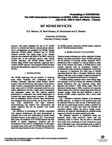
MEMS ON CONTOUR SUBSTRATES We propose to fabricate MEMS devices directly onto contour mechanical parts. We have developed a fabrication technology which allowed us to align and pattern multiple layers of thin films on mechanical substrates of selected contours. Initial results show that -5pm width/gap resolution is possible on a 2” long quartz cylindrical substrate of 1.25” diameter. Measurement of microstructure dimensions on the curved surface was made possible using the Wyko Surface Profiler (white-light interferometer). Some representative structures on the cylindrical surface are shown in Figure 1 below, To the best of our knowledge, direct fabrication of microstructures onto non-flat surfaces have only been investigated by Jacobsen et. a1.[4], Ogura et. a1.[5], and Jackman et. a1.[6] (and the related work from Harvard). However, their processes were developed without any need for alignment of different thinfilm layers. Also, the efforts of Jacobsen and Ogura have concentrated on substrates of millimeter scale. The techniques for thin- film deposition, lithography, and alignment on the bulk cylindrical substrate are discussed in this paper.
Figure 1. Interferometer image of representative structures on the cylindrical surface. The dimensions given in thefiinge image are in pm.
1431
PROCESS TECHNOLOGY We have developed a process to produce flexible
TRANSDUCERS ’97 1997 international Conference on Solid-state Sensors and Actuators Chicago, June 16-19, 1997
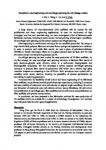
4D2.09P masks which can conform to selected curved surfaces. With a custom designed alignment system, these masks can be utilized to transfer patterns onto contour surfaces employing optical exposure methods used in standard IC processing. Flexible Mask Flexible masks were made by evaporating thin metal films such as Au and Cr onto a flexible material which can survive acetone, developer, and metal etchants. The thin metal films are then patterned by standard lithographic techniques using conventional high resolution masks. Minimum widtwgap resolution of -2pm on the flexible mask can be obtained by this technique. If the flexible masks are directly patterned by E-beam writing submicron resolution should be possible. Aside from surviving the typical chemicals used in mask making, the flexible material must also have low thermal coefficient of expansion (TCE). Significant difference in TCE between the metal films and the flexible material can create sufficient thermal residual stress during metal evaporation and cause cracks in the thin metal films. Figure 2 shows smooth and cracked thinfilms on the flexible masks.
Figure 2. (a) Flexible mask with low TCE substrate material. (b) Flexible mask with relatively high TCE substrate material. Note the cracks in the thin CrJilm. The cracks are typically -0.2pm in width.
0.6pm and standard deviation of 0.16pm. The 3D image shown in Figure 3a was obtained by converting the 2D interferometer contour data using a sofhvare supplied by Wyko.
10
09
g
08
2
07
k
06
B
‘9 0.5
9
0.4
d 0.3 I
0.2
. .
0.4
I
0.6
0.8
I 1.0
Photoresist Thickness,(JNU)
Figure 3. (a) 3 0 interferometer image of resist structure used for resist uniformity analysis. (3) Cumulative distribution of the resist thickness around the cylinder.
Alignment Scheme Similar to flat substrate alignment, there are 3 possible adjustment errors when aligning a conforming mask to a pre-patterned cylinder. These errors are rotational, translational, and yaw as illustrated in Figure 4. Also shown in Figure 4 are the alignment systems we have developed to adjust these errors. A system is first used to adjust the yaw error between the cylinder and the mask. The mask is then secured to the cylinder by an anchor which allows the mask only to move axially and circumferentially about the cylinder. The anchored mask and the substrate is then transferred to a second system for rotational and translational alignment.
Spraying of Photoresist
Sacrificial Release Process
We have elected to coat photoresist onto the cylindrical substrate by spraying. Dip-coating is a widely used technique for coating cylindrical substrates but will consume more resist than the spraying method and can not be used for other generalize curved surfaces. A commercial airbrush system was used to spray low viscosity photoresist onto the cylindrical substrates. Thirty samples of the 20pm lines shown in Figure 3a were measured randomly around a cylinder to statistically analyze the resist uniformity. The cumultive distribution function of the samples is shown in Figure 3b. The resist thickness distribution is Gaussian with mean of
To validate the alignment scheme we have designed a simple 3-mask sacrificial release process to fabricate microstructures suitable for use as sensors and actuators. The first mask defines the electrical interconnects and bonding pads; the second mask defines the via through the sacrifical layer; the third mask patterns the sensor and actuator structures. The above process was optimized on flat Si substrates prior to cylindrical substrate fabrication. Au was used as the interconnect metal with Cr as the adhesion layer between Au and the substrate. Photoresist was used as the sacrificial layer and was removed using resist-stripper during the sacrificial release process.
TRANSDUCERS ‘97 1997 hiernational Conference on Solid-state Sensors and Actuators Chicago, June 16-19, 1997
1432
4D2.09P
align m en t
yaw alignment
Figure 4. Possible positioning errors between the cylinder and the flexible mask. Yaw error is adjusted before rotation and translation alignment.
Ti and Au were used as the structural materials. Ti was mainly used to stiffen the structures and create simple thermal bimorphs when combined with Au. The cylindrical substrates were rotated during Ebeam metal evaporation to ensure uniform thinfilm thickness about the substrate. Figure 5 illustrates the process described above. For the metal electrical contact layers 500A of Cr and 3000w of Au were used. For the structural layers 2000w of Ti and 8000A of Au were used.
Figure 5. Metal structural layers and sacrijkial material used for a simple 3-mask process to make sensors and actuators on the cylinder.
CURRENT RESULTS Thermal Bimorph Actuators on a Flat Substrate Various thermal and electrostatic actuators were made on a flat Si substrate using materials shown in Figure 5. Figure 6 shows a representative thermal bimorph actuator on a flat substrate. The ratio of thicknesses between Ti and Au for the structural layers is critical. Excessively thick Ti layer can cause Joule burn out of the bimorph before adequate thermal strain force can be induced to actuate the structures. Insufficiently thick Ti layer can cause low yield of the micro devices during the wet sacrificial release process. We have found that using 2000A of Ti and 8000A of Au for the structural layers can allow over 90% yield on a 3” wafer for structures >10pm wide. Using the same thickness ratio, motion can be initiated on a bimorph actuator with 500pm long 20pm wide arms using -1mA current. Tip deflection of the thermal bimorphs versus current can be approximated by coupling the equations of thermal strain and of Joule heating on a 2-layer beam clamped on one end[8]. Figure 6 also shows the comparison of experimental and theoretical results. Theoretical analysis showed that heating dominates in the Ti layer due to its higher resistivity and smaller cross-sectional area when compared to the Au layer. In addition, heat dissipation of the structures occurs mostly through the substrate and the convection term can be neglected in the energy
1433
TRANSDUCERS ‘97 1997 International Conference on Solid-state Sensors and Actuators Chicago, June 16-79, 1997
4D2.09P balance equation. The lower theoretical prediction for the tip deflection at higher currents can be attributed to the assumption of invariability of resistivity with temperature. In reality, resistivity of the metals will increase as temperature increases, resulting in further expansion of the beam. 250 225
5 6
.-0 5
200
175 150 125
P)
100
0
9.
75
0
0.02
0.04
0.06
0.08
0.1
0.12
0.14
0.16
Applied Current, (A)
Figure 6. Sample bimorph actuators on a f l a t Si substrate. Theoretical values were obtained using Re$
Figure 7. Interferometer image of sacrijkially released structure on a quartz cylindrical substrate.
PI. Sacrificially Released Structures on the Cylinder Using the previously described 3-mask process sacrificially released structures were fabricated on a quartz cylindrical substrate. Figure 7 shows an interferometer image of a released structure which is hanging above another released structure that was bent during the wet-release process and trapped under the first structure. We have begun to test these structures as thermal actuators. Structures which are clamped at both ends and suspend -0.5pm above the cylinder surface were also fabricated and will be tested as shear-stress flow sensors. CONCLUSION We have developed a fabrication technology to directly fabricate MEMS devices onto non-silicon macro cylindrical substrates. Similar to standard IC processing, this technology uses flexible masks and novel alignment systems to optically transfer pattems to the macro substrate . With the current alignment system structures can be fabricated -350" circumferentially around the cylinder. Preliminary results indicate that -50% yield is possible for structures -5pm. The yield increases to -90% for structures -20pm. We have sacrificially release metal structures on a 1.25" diameter 2" long quartz cylindrical surface. We are current testing these structures as thermal sensors and actuators and the results will be reported in the near future.
TRANSDUCERS '97 1997 lnfernafionalConference on Solid-state Sensors and Actuators Chicago, June 16-19, 1997
ACKNOWLEDGEMENT We would like to thank the Micro Devices Laboratory at JPL for the usage of various process equipment. We are indebted to Mr. Edward Fortier 111 for his remarkable technical skills and invaluable suggestions on building and refining the mechanical systems needed for fabrication. Special thanks also to Dr.Tony Tang for the usage of the interferometer.
REFERENCES [I] C. M. Ho, et. al., Control of Macro Machine by Micro Actuators, Bulletin of 47th Annual Meeting of the Division of Fluid Dynamics of the American Physical Society, Atlanta, Georgia, USA, November 1994. [2] S. C. Jacobsen, MEMS PI Meeting Report, Sarcos Research Corporation, July 1995 through January 1996. [3] C. M. Ho, Y . C. Tai, and D. Miu, Conformable M3 Microsystems for Aerodynamic Control, Semi-Annual Report for ARPA, UCLNCIT, January 1995 through July 1995. [4] S. C. Jacobsen, et. al., Fabrication of Micro-Structures Using Non-Planar Lithography, MEMS 1991, pp 63-67. [5] H. Ogura et. al., A Concentric Build-up Process to Fabricate Practical Wobble Motors, M E M S 94, pp. 114118. [6] R. J. Jackman et. al., Fabrication of Submicrometer Features on Curved Substrates by Microcontact Printing, Science, Vol. 269,4 August, 1995, pp. 665-665. [I] W. J. Li, UCLA MAE Dept. Ph.D. Prospectus, January 1997.
1434