FRBOR03
Proceedings of RUPAC2012, Saint|-|Petersburg, Russia
NON-GATED FIELD EMISSION ARRAY AS LOW-ENERGY ELECTRON SOURCE: EXPERIMENT AND SIMULATION K.A. Nikiforov∗ , L.I. Antonova, N.V. Egorov, V.V. Trofimov, St. Petersburg State University, St. Petersburg, Russia V.V. Makeev, O.F. Ogurtsov, Molecular Electronics Research Institute, Zelenograd, Russia Abstract A non-gated NbN on Si wafer field emission arrays are studied. The I-V measurements and emission characteristics of edge-shaped cathodes in atmosphere low-voltage regime are considered. Mathematical and computer models are presented. The current density obtained from experiment was up to 384 Ampere per square centimeter in emission area 9 mm2 . Low-voltage regime (20 V) for near (∼1 μm) interelectrode distance in diode configuration is discussed. High-voltage operation in high vacuum was experimentaly studied and preliminary results are discussed.
PULSED LOW-VOLTAGE OPERATION IN ATMOSPHERE Experiment An ungated NbN field-emitter array was placed at atmospheric pressure in a close-diode configuration with a planar anode with area 9 mm2 . The anode-cathode gap was set 1 μm using precision dielectric spacers shown in Figure 2.
c 2012 by the respective authors — cc Creative Commons Attribution 3.0 (CC BY 3.0) Copyright ○
BACKGROUND The standard emission mechanisms of the cathodes used in the accelerator electron guns are photoemission and thermionic emission. One alternative technology is fieldemitter arrays (FEA) where electrons are emitted with energies close to the Fermi level. Such cathodes have potentially a lower mean transverse kinetic energy of the produced electron beam, which is mainly determined by the geometry of the electric field lines. We present first measurements on commercial field-emitter arrays in atmosphere pulsed low-voltage operation and DC high-vacuum high-voltage regime as well as numerical simulations of the electric field near the cathode surface. There are 2 main architectures of field-emission cathodes: (i) the needle cathode, i.e. one single sharpened tip and (ii) FEA which are arrangements of field emitters on a periodically spaced lattice. In these proceedings we consider FEA with axialsymmetric emitters of sharp edge type. The photo and SEM image in Figure 1 represent 1 × 1 cm cathode in pincers with NbN thin-film emitters on heavy As-doped Si wafer from JSC Mikron.
Figure 1: FEA 1 × 1 cm (left) with ∼4000000 NbN emitters (right).
∗ nikiforov
[email protected]
Figure 2: SEM picture of 1 μm height spacers on cathode surface. The anode was heavy As-doped Si plate electrically isolated from ground and pressed close to cathode by probe tungsten tip of micromanipulator, 300 μs voltage pulses at low frequency was applied. A 100 Ω resistor was placed in series with the cathode and attached to a sensitive voltage meter. A schematic of the experimental configuration is shown in Figure 3.
Results The field emission characteristics of the system are shown in Figure 3, as a function of bias voltage.
Figure 3: Field emission current and current density vs. cathode voltage. Insert: a schematic of the FEA cathode, emitters, spacers and anode used to collect the field emission.
ISBN 978-3-95450-125-0 218
Ion sources and electron guns
Proceedings of RUPAC2012, Saint|-|Petersburg, Russia
DC HIGH-VOLTAGE OPERATION IN HIGH VACUUM
FRBOR03
mity was improved, turn-on field was decreased, and current fluctuations due to adsorbate diffusion were reduced.
Experiment
Figure 5: Fowler-Nordheim plots of emission characteristics before and after discharging. Insert: pictures of luminophore anode during and after the experiment. Figure 5 represents the emission current measured between FEA cathode and luminophore anode when increasing DC voltage was applied. The gap between electrodes was 1.5 mm. Temporal and spacial unstability were observed again when voltage reached 9 kV and current∼0.05 A. Tracks of some destructive arcs were visible on anode surface when cathode had been moved away after the experiment. Squere shaped tracks (shown in Figure 5) opposite FEA cathode edges are cased by fringe effects of electric field gain.
DISCUSSION AND NUMERICAL SIMULATION
Figure 4: (left) High voltage vacuum chamber and field emission test stand used for evaluating FEA cathode, (right) anode, FEA cathode turned round in horizontal plane, resistance-type heater and TiO2 /Cs sources inside the chamber.
Results When a FEA was initially turned on, the emission was nonuniform and the observed beamlets underwent flickering, presumably due to the diffusion of weakly bound adsorbed species. Over time, following voltage increasing, the weakly bound species were removed from the cathode and the tightly bound adsorbates performed a pseudorandom walk toward the region of highest field, the emitter edge. These adsorbates may enhance the emission by dipole lowering of the local surface-energy barrier, resonant tunneling, or other effects. Therefore emission unifor-
Ion sources and electron guns
Historically, one of the most significant barriers to the adoption of FEA technology has been the difficulty of providing uniform emission current over a large spatial extent. The emitted current is extremely sensitive to emitter properties such as geometry, work function, and surface contamination. Small fabrication variations in emitter tip radius, height, chemical composition, and crystalline orientation can result in order of magnitude differences in the emission current between tips in a FEA. Additionally, the strong electric field gradient near the cathode attracts polarizable species from the vacuum to the cathode surface. The induced dipole moment of an adsorbate can significantly lower the local surface energy barrier for emission. Also, adsorbate effects such as resonant tunneling may produce order-of-magnitude enhancements in the local emission current. The varying emission levels from tip to tip result in different local surface temperatures through Joule heating. This spread in temperature leads to fundamentally different contamination states for various tips in the ensemble. In this section we first consider the physical explanation the law of the electric field gain on emitters according to ISBN 978-3-95450-125-0
219
c 2012 by the respective authors — cc Creative Commons Attribution 3.0 (CC BY 3.0) Copyright ○
The apparatus is shown in Figure 4. Experiments were performed in a high vacuum chamber with a base pressure of about 5 · 10−8 Torr. The system is capable of applied voltages up to 15 kV. Prior to the application of high voltage, the FEA was baked at ∼100◦ C for approximately 1 hour to prevent local pressure rising during experiment. In DC operation the limiting factor for high current emission in FEAs is the thermally induced desorption of atoms and the related contamination and sputtering problems. These well-known environmental problems can lead to current emission fluctuations by changing either the work function or the tip geometry [1]. Local pressure rise can even lead to some destructive arcs. Therefore A 100kΩ conditioning resistor was placed in series with the cathode FEA and served to protect the apparatus in case of sudden discharge of stored energy. The cathode could be horisontally moved/rotated to vary the cathode/anode gap and therefore the field gradient. A flat luminophore anode was parallel placed 1.5÷3.0 mm away from cathode FEA and large voltage (kilovolts) was applied.
c 2012 by the respective authors — cc Creative Commons Attribution 3.0 (CC BY 3.0) Copyright ○
FRBOR03
Proceedings of RUPAC2012, Saint|-|Petersburg, Russia
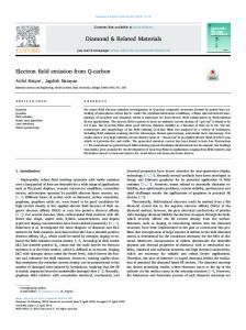
[2]. As it is shown in Figure 5 fringe effects play negative role in emission uniformity while gap between electrodes is relatively large (∼1 mm). Electric field gain at FEA edges is very high that does not allow rise voltage sufficient to turn on middle FEA emitters: only extreme emitters operate at FEA edges and higher voltage causes destructive (maybe explosive) effects on them. Thus maximal emission current density observed in experiment was limited by power dissipation in vacuum chamber. Moreover in case of near interelectrode distances there is not fringe effects, therefore maximal current density observed in experiment has remarkable value 384 A/cm2 (we can not evaluate improved uniformity because the anode has not luminophore in this case, but high maximum of current values indirectly indicates this fact). To calculate the electric field gain “zooming” algorithm has been used. According to this algorithm at the first stage the field gain is calculated over whole area of FEA under consideration using the net with the large enough pitch so only squere shape of FEA is considered. At the second stage the field is calculated more accurately over the less area including emitters and using the net with less pitch (relative to the whole area) and the boundary conditions being defined from the solution obtained at the first step. In case of near interelectrode distance (∼1 μm, first experiment) let k2 is protrusive emitters magnification factor of planar capacitor uniform field E0 formed by electrodes surfaces (in smooth geometry approximation). If gap between electrodes is relatively large (∼1 mm, second experiment) electric field E0 is additionally magnified due to fringe effects. Let k1 is magnification factor in this case. Thus electric field in emission area is E = k2 E0 in first experiment and E = k1 k2 E0 in second experiment. Program complex for vacuum nanoelectronics simulations [3] based on Matlab Partial Differential Equation Toolbox has been used for calculating the value k2 . The electrostatic field calculated at the second stage has got equipotentials shown in Figure 6. The field gain of the second step has got the value which changes along the surface of the emitter’s top, max(k2 ) = 3.5.
Figure 6 provides a view of the equipotential plot around the emitter, when the bias condition is set as 0 V on the cathode and 12 V on the anode. The contours around the top of emitter in Figure 6 indicate the zones at which the electric field distribution is constant. The contours that have been plotted include magnitudes of ≈5 to 30 V/μm in increments of 1 V/μm and do not denote the direction of the electric fields. The magnitude of the electric field defined by each contour scales linearly with respect to the anode voltage. Factor k1 has been found from finite element analysis in Comsol Multiphysics. 3D electrostatic problem has been solved in large sphere bounded domain. Electrodes were located in sphere centre. Constant-electric field distribution contours around the cathode edges are presented in Figure 7. The inner and outer countours matche the electric field of 3.5 V/μm and ≈5.5 V/μm at anode voltage 3 kV , i.e. 70% and 110% of planar capacitor field E0 respectively: k1 ≈ 1.1.
Figure 7: Constant-electric field distribution contours around the FEA cathode edges.
CONCLUSION Preliminary results on peak current performance of field emitter array sample in atmosphere and high-vacuum during pulsed and DC operation at low- and high-voltages showed that higher values and more stable current can be emitted with anode near location at distance ∼1 μm and voltage ≤20 V. Fringe effects play negative role in emission uniformity while gap between planar electrodes and voltage are relatively large (∼1 mm and ∼103 V). Electric field gain in this case has got the value 110% at cathode edges. This value is quite essentially due to exponential dependence of emission current density vs. applied voltage. FEA is considered as low-energy electron source. The future work involves spherical anode compensating fringe effects.
REFERENCES [1] P. R. Schwoebel, et al., J. Vac. Sci. Technol. B 19 (2001) 582. [2] V. A. Solntsev, A. N. Rodionov, Solid-State Electronics 45 (2001) 853.
Figure 6: (left) Equipotential line plot of cylindrical field emitter cell in diode configuration at a given bias condition (only one half of cell is shown in cylindrical coordinates due to axial symmetry), (right) electric field distribution around the emitter. Insert: constant-electric field distribution contours around the top of a cylindrical emitter.
[3] K. A. Nikiforov, N. V. Egorov, “Program Complex for Vacuum Nanoelectronics Finite Element Simulations” TUPPB043, these proceedings.
ISBN 978-3-95450-125-0 220
Ion sources and electron guns