Traditional power optimization and estimation tech- niques for digital CMOS circuits have focused on the dynamic power dissipation, caused by charging and dis ...
On Short Circuit Power Estimation of CMOS Inverters� Qi Wang and Sarma B.K. Vrudhula Center for Low Power Electronics Department of Electrical and Computer Engineering The University of Arizona, Tucson, AZ 85721
Abstract
300
Traditional power optimization and estimation techniques for digital CMOS circuits have focused on the dynamic power dissipation, caused by charging and discharging the load capacitances at the gate outputs. However, as the device size and threshold voltage continue to decrease, the short circuit power dissipation is no longer a negligible factor. We show that previously published models for the short circuit power can not provide the accuracies required for current technologies. To improve the accuracy, we propose a new semi-empirical short circuit power model. Comparison of the porposed model with HSPICE simulation results on CMOS inverters using the Rockwell 0.25 �m CMOS process parameters show that proposed model is signi cantly more accurate for estimating the short circuit power than the models reported in the literature.
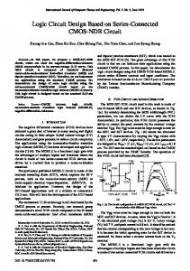
250
Psc/Pd (%)
200
150
100
50
0
0
50
100
150
200
250
300
350
CL (fF)
Figure 1: Short circuit power dissipation (Psc ) as a percentage of dynamic power dissipation (Pd ) for the CMOS inverter shown in Figure 3. Assume input transition time �0 =2 ns and f = 100 MHz.
1 Introduction
Reduction of power dissipation in CMOS digital circuits has become an increasingly important design optimization goal. Although there are several sources of power dissipation in the CMOS technology, most of the existing power optimization and estimation techniques have focused on the dynamic power dissipation (Pd = CL Vdd2 f ), due to the charging and discharging the load capacitances at the gate outputs. The other major source is the short circuit power dissipation (Psc ) which is due to the simultaneous conduction of the PMOS and NMOS transistors during the input transitions. However, as the device size and threshold voltage become smaller, Psc is no longer a negligible factor. For example, for high performance circuits, if large gates are used to drive relatively small loads and if the input transition time is long, then Psc becomes quite signi cant [1]. Figure 1 show a plot of Psc =Pd for a CMOS inverter with minimum channel length of 0.25 �m for di�erent load
capacitances. The plot was obtained using HPSPICE. It can be seen that in some cases, e.g., when the load capacitances are small, the short circuit power dissipation can far exceed the dynamic power dissipation. In this paper we address the problem of short circuit power estimation of a CMOS inverter. Since the original work by Veendrick [2], di�erent models have been proposed for short circuit power estimation with di�erent levels of accuracy. It is well known that the Psc depends on input signal transition time, load capacitance and transistor sizes. The model proposed in [2], ignores the load capacitance at the gate output and assumes that the saturation short circuit current ows from VDD to GND during the entire transition period. This model results in an upper bound of the Psc of a CMOS inverter. Consequently, it only provides a qualitative measure of the Psc and is not su�ciently accurate for power estimation and optimization. In [3], a more realistic Psc model, which includes both the e�ects of input transition time and output load capacitances, was proposed. In the rest of this paper, this model will be referred to as the HJ model. It was shown that for normal opera-
� This work was carried out at the Center for Low Power Electronics which is supported by the National Science Foundation, the Department of Commerce of the State of Arizona, and several sponsors from the the microelectronics industry, including, Analog Devices, Analogy, Burr Brown, Rathyeon, Intel, Microchip, Motorola, National Semiconductor, Rockwell, Sicom, SMI, Texas Instruments, and Western Design.
1
As stated above, Equation (2) provides an uppert bound on Psc . However, comparing (1) and (2), when tHL;o LH;i < 3, the average current obtained by (1) may exceed the maximum average short circuit current given by (2). Additionally, due to the non-linearity of the input and output waveforms in practice, the input and output slope are normally estimated from the real input and output transition time. Therefore the accuracy of (1) is strongly depended on the choices of tHL;o and tLH;i . HSPICE simulation shows that the short circuit power obtained from Equation 1 are overestimated in most cases. It should be noted that none of above mentioned models have been validated for modern deep submicron technology. In this paper, we present a new semiempirical model for Psc which is demonstrated to be accurate for a wide range of device parameters for modern deep submicron technology. The model is validated by experiments on di�erent con gurations of CMOS inverters from a commercial 0.25 �m CMOS technologyWe gratefully acknowledge Dr. Tom Dillinger of Rockwell for providing us with their 0.25 �m model. The rest of the paper is organized as follow. In Section 2 the derivation of the new model is presented. The experimental results are shown in Section 3. The conclusions and directions for future work are given in Section 4.
40
Short circuit power (microW)
35
30
o HSPICE
25
− HJ Model
20
15
10
5
0
50
100
150
200 CL (fF)
250
300
350
400
Figure 2: Comparison of the short circuit power dissipation of the CMOS inverter in Figure 3 between HSPICE simulation and HJ model. Assume input transition time �0 =5 ns, and f = 100 MHz. tion, the short circuit power dissipation of an inverter is only 30% of the amount predicted by the model in [2]. Unfortunately, this model is also not su�ciently accurate for current submicron technologies. Figure 2 shows the comparison between the HJ model and the HSPICE simulation for the simple inverter shown in Figure 3. It can be seen that for slow input and fast output signals, the error between the model and simulation can be as large as 100%. The work by [4] improved the results of [3] by considering the short channel e�ects in the current equation. However, to obtain closed form formulae, impractical assumptions had to be made that lead to signi cant errors under certain conditions. Additionally, in the formula to Psc an evaluation of gamma function is required which is too computational expensive in practice. More recently a new short circuit power model was proposed by [5]. The approach taken was to model the short circuit power by determining an equivalent short circuit capacitance. Assuming linear input and output waveforms, the authors of [5] found that the average short circuit current during the input rising transition is given by (1): 1 2 (1 ? b)2 (1) Iavg (p) = 6p VDD 1 + ttHL;o LH;i
2 The proposed model All the short circuit current models mentioned in Section 1 except [4] were based on the classic Shichman and Hodges [6] model for the MOSFET. This model is not suitable for short channel MOSFETs. The work by [4] was based on a more accurate short channel current model but it leads to di�culties in deriving closed form formulae for Psc . In fact, to obtain a closed form formula for Psc , the authors [4] had to make assumptions that result in signi cant departure from the HSPICE simulations. However, as to be pointed out in the next section, the main reason for the errors in all these Psc models is not due to the inaccuracy of the MOSFET current models. Instead the main reason for the inaccuracy is due the fact that the current in the PMOS (NMOS) device is ignored during the rising (falling) transition on the input. To develop a simple yet accurate Psc model for modern deep submicron technology we propose the following approach. The Shichman and Hodges [6] MOSFET current model is still used due to its simplicity. However, a closer scrutiny of the errors in the model, they will be accounted for through the introduction of technology dependent parameters. Figure 3(a) shows a simple CMOS inverter. Without loss of generality, we analyse the situation where there is a 0 to 1 transition at the input and the corresponding output goes from 1 to 0. An ramp input with transition
where tLH;i and tHL;o are the input and output slopes respectively, and b = (Vt;n + jVt;p j)=VDD . On the other hand, using the technique in [2], the average short circuit current during the input rising transition can be expressed as (2): 2 (1 ? b)2 Iavg (p) = 24p VDD
(2) 2
where E10 and E01 are the high to low and low to high output transition probabilities respectively. The average short circuit current for the output low to high transition In;avg can be derived analogously. Without loss of generality, in the following discussion we will focus only on the derivation of Ip;avg . Based on Equations (4), (5) and (6), the key to determining Psc , is to determine vout as a function of t in T1 , from which the value of t2 can be obtained. Note that for a rising input ramp, when the PMOS transistor is in the linear region (i.e. t 2 T 1), the NMOS must be in the saturation region. Therefore the corresponding output response can be determined from the following di�erential equation
v Vdd
1 v3
1.5/0.25
v2
Vout
Vin 0.5/0.25
v in
v out
CL v1 0 t1 t2 t3
(a)
t
(b)
Figure 3: (a) A CMOS inverter (b)The input and output voltage during a high to low transition at the output.
? VCL dvdtout = 2n (vin ? n) DD ? p [(vin ? 1 ? p)(vout ? 1) ? (vout ? 1) ] (8) 2
1 2
time �0 is assumed. For simplicity, all the voltages are normalized with respect to VDD . The input voltage from 0 to �0 can be written as
vin (t) = �t ; 0
t 2 [0; �0 ]:
To obtain an expression of vout , we start with the same approach taken by previously published models, i.e., we assume that the current owing through the PMOS transistor is negligable in comparison to the current owing through the NMOS transistor. As a result, Equation 8 can be simpli ed to
(3)
In Figure 3(b), t1 and t3 are the times when the gateto-source voltage of the NMOS and PMOS transistors reach their respective threshold voltages, i.e., t1 = n�0 and t3 = (1 + p)�0 , where n and p are the normalized NMOS and PMOS threshold voltages respectively. Note that p is negative. t2 is the time when the PMOS transistor moves from the linear to the saturation region. Let T1 = [t1 ; t2 ] and T2 = [t2 ; t3 ]. The short circuit current for an output high to low transition is the current that ows through the PMOS transistor in T1 and T2 . Using the Shichman and Hodges model [6], these are given by 2 p [(vin ? 1 ? p)(vout ? 1) ? 21 (vout ? 1)2 ]; Ip;T (t) = VDD (4) 2 p 2 Ip;T (t) = VDD 2 (vin ? 1 ? p) ; (5) where p and n are the PMOS and NMOS gain factors respectively. Therefore the short circuit current for the high to low output transition averaged over one clock period is given by
? VCL dvdtout = 2n (vin ? n) : 2
DD
n �0 t 3 vout = 1 ? VDD 6C ( � ? n) : L
Let Rn = pressed as
Ip;avg = [ Ip;T (t)dt + Ip;T (t)dt]f; 2
1
t1
1 (VDD n )
0
(10)
. Then Equation (10) can be ex-
(11) vout = 1 ? 6R�0C ( �t ? n)3 : n L 0 If we normalize all times by Rn CL , vout can be expressed as 0 vout = 1 ? 61 �0 0 ( �t 0 ? n)3 ; (12) 0
2
Zt3
(9)
The output voltage can then be found to be [3]
1
Zt2
2
where
�00 = R �C0 ; n L
t0 = R tC : n L
(13)
The term Rn CL is the time constant for discharging the output load capacitance CL through the NMOS transistor. Thus, �00 can be interpreted as the ratio of the input and output transition time. Ignoring the current through the PMOS transistor during input rising transition (as was done with all previous models) lead to large inaccuracies in vout . In fact, this current can be very large, making it comprable to the current through the NMOS transistor, when �00 is large. When �00 is large, the input transition time is much longer than the output transition time and the PMOS transistor will be on
(6)
t2
where f is the frequency of the input waveform. The average short circuit power dissipation for a CMOS inverter is obtained by taking the weighted sum of the current through the PMOS and NMOS transistors. This is given by Psc = VDD (Ip;avg E10 + In;avg E01 ); (7) 3
for a much longer duration. Furthermore, when CL is relatively small, �00 will be large, and the output voltage will drop faster in comparison to when �00 is small. This results in the PMOS transistor staying in saturation for a longer period. Both of these factors will increase the current of PMOS during the input rising transition. As a result, the discharge current of CL will be overestimated when (8) is replaced with (9) by assuming that the current through the PMOS transistor is zero. This will result in an under estimating vout , which in turn leads to an over estimate of Ip;avg in (6) and Psc in (7) 1 . Note also that the short circuit current of PMOS transistor can also be comparable to the current through the NMOS transistor when p is large. One way to include the e�ect of the PMOS transistor on the short circuit current is to include p in Equation 12. Toward this end, we propose the following model for vout . 0 (14) vout = 1 ? 61 �0 0 �( �t 0 ? n)3 0 � = � 0 � p + � 1 : (15) �0 and �1 are technology dependent parameters and � is less than 1. The reasoning behind this approximation can be explained as follows. Based on the earlier analysis, the actual value of vout will always be greater than the one predicted by (10), especially when �00 and � 0 0 p are large. By replacing �0 by �0 , where � < 1, the vout in (14) will become larger than the one in (10). Furthermore, if � decreases with increasing p , then the current through the PMOS transistor will increase, as is required. For this reason, we expect �0 < 0. Using (14) for vout , t2 can then be easily determined by substituting vout = vin ? p (point at which the PMOS transistor moves from the linear region to the saturation region) into (14). There is only one solution to the cubic equation of (14) which results in the following value for t2 .
p
q
t2 = 3 a [ 3
p
1+ 2 1+
1
a
27
q
3 2+
p
?2
1
1+
0
0
1
3 Experimental Results To examine our model we conducted experiments on a few CMOS inverters with di�erent con gurations using the Rockwell 0.25 �m CMOS process. The parameters in the proposed Psc model were obtained by tting the model with the HSPICE simulation results and are shown in Table 1. The device models used in the HPSICE simulation are BSIM3 level 49. Four di�erent input ramps were simulated, i.e. �0 = 1ns, 2ns, 4ns and 5ns. For each input ramp, the load capacitance CL was varied from 10 fF to 355 fF. PMOS transistors with three di�erent channel widths, i.e. Wd = 1:5�m; 2:5�m; 3:5�m were used. The operational frequency was chosen to be 100 MHz, which is su�ciently large for all signal to stablize before the next clock cycle.
�0 V 2 =A
3
+
(1
5
2
�1 A � sec
Figures 4 to Figure 6 show the results of the HSPICE simulation and the values predicted by the proposed model. The Figure 7 shows the comparison of the HSPICE simulation, the proposed model and the HJ model for all data points that were collected. From all these gures, it can be seen that the proposed model matches HSPICE simulation quite well for all con gurations. A summary of the statistics of the proposed model and HJ model results is shown in Table 2. The average error, compared to the HSPICE simulation, of the new model is only 6.3%, which is much less than the 61.8% error of the HJ model. More importantly, from the value of the standard deviation, it can be concluded that the new model predicts Psc within 10% of HSPICE simulation.
?2n) �4 ? �5 ? 2 �7 ] 4
�0
Table 1: Model parameters.
where = 61 �00 � and a = 1?22n . Substituting (14) and (16) into (6), the average current can be expressed as 2 Ip;avg �VDD p �00 Rn CL f [ (1?2n6?�)
�1
unit None (V=A) � sec value -2.4E+2 0.8 9E-12 0.46E-14
(16)
a2 ]�0 +n�0
27
simulation, we nd that even when �0 = 0 the average current is not zero. This is because the model does not consider many other second order e�ects, e.g. the Miller e�ect of the gate-drain capacitance. To model this nonzero short circuit current, we use the following formula to represent the average short circuit current: ~ + �I � f Ip;avg = Ip;avg (18) where �I = � 0 � p + � 1 (19) �0 and �1 are the two technology dependent parameters to be determined from the simulation. The average short circuit current for the output low to high transition can be analogously determined by replacing p in (17,19) by n and n in (13) by p .
14
(17) where � = t2 ? n�00 . From Equation (17) it can be seen that the average short circuit current will decrease with the increase of CL and �0 . Ideally, when �0 = 0 or CL = 1, the short circuit current will be zero. However, from the HSPICE 1 This also explains the errors of Equation 1 in Section 1. By assuming vout to be a linear slope instead of a non-linear waveform in reality, the output voltage may be signi cantly underestimated which leads to the overestimation of the average short circuit current.
4
35
30 o HSpice (τ0 = 5ns) * HSpice (τ0 = 2ns)
25
35
HSpice (τ0 = 1ns) 30
lines Model
o HSpice (τ0 = 5ns)
20
15
10
5
+ HSpice (τ0 = 4ns) HSpice (τ0 = 1ns)
* HSpice (τ0 = 2ns)
25 Short circuit power (microW)
Short circuit power (microW)
+ HSpice (τ0 = 4ns)
lines Model 20
15
10 0
0
50
100
150
200 CL (fF)
250
300
350
400 5
Figure 4: Comparison of the new model and the HSPICE simulation for the the CMOS inverter in Figure 3 with PMOS channel width of 1.5 �m.
0
0
50
100
150
200 CL (fF)
250
300
350
400
Figure 6: Comparison of the new model and the HSPICE simulation for the the CMOS inverter in Figure 3 with PMOS channel width of 3.5 �m.
35
30 o HSpice (τ0 = 5ns)
HSpice (τ0 = 1ns)
* HSpice (τ0 = 2ns)
25 Short circuit power (microW)
+ HSpice (τ0 = 4ns)
lines Model 20
15 100
10
0
0
50
100
150
200 CL (fF)
250
300
350
Short circuit power (microW)
5
400
Figure 5: Comparison of the new model and the HSPICE simulation for the the CMOS inverter in Figure 3 with PMOS channel width of 2.5 �m.
90
solid lines:
New model
80
dotted lines:
HJ model
70
markers (+):
HSPICE
60
50
40
30
20
10
0
New Model HJ model Maxium error 22.7% 188.9% Average error 6.3% 61.8% Standard deviation 6.7% 41.0%
0
20
40
60
80
100 Data points
120
140
160
180
200
Figure 7: Comparison of the HJ model, the new model and the HSPICE simulation for the the CMOS inverter in Figure 3.
Table 2: Statistics of our model v.s. HSPICE simulation for the CMOS inverter in Figure 3. 5
4 Conclusion Power estimation and optimization for deep submicron CMOS logic circuits requires accurate modeling of short circuit power dissipation [7]. In this paper we presented a new model for the short circuit current of CMOS inverters that is suitable for modern deep submicron technology. Experimental results show that the proposed model matches HSPICE simulation results much better than previous models. One of the future directions of this work is to relate the model parameters to MOSFET physical parameters. Work on extending the model to other more complicated CMOS gates and applying the proposed Psc model to circuit power optimization is currently in progress.
References [1] M. Pedram \Power Minimization in IC Design: Principles and Applications," ACM Trans. on Design Automation and Electronic Systems, vol. 1, No. 1, January 1996, pp. 3-56. [2] H. J.M. Veendrick \Short-Circuit Dissipation of Static CMOS Circuitry and Its Impact on the Design of Bu�er Circuits," IEEE Journal of SolidState Circuits, Vol. sc-19, No. 4, August 1984, pp. 468-473. [3] N. Hedenstierna and K. O. Jeppson \CMOS Circuit Speed and Bu�er Optimization," IEEE Trans. on Computer-Aided Design, Vol. CAD-6, No. 2, March 1987, pp. 270-281. [4] S. R. Vemuru and N. Scheinberg \Short-Circuit Power Dissipation Estimation for CMOS Logic Gates," IEEE Trans. on Circuits and Systems I: Fundamental Theory and Applications, Vol. 41, No. 11, November 1994, pp. 762-765. [5] S. Turgis, N. Azemard and D. Auvergne \Explicit Evaluation of Short Circuit Power Dissipation For CMOS Logic Structures," Proceedings of Internation Symposium on Low Power Design, 1995, pp. 129-134. [6] H. Shichman and D. A. Hodges, \Modeling and simulation of insulated gate eld e�ect transistor switching circuits," IEEE J. Solid-State Circuits, vol. SC-3, Apr. 1990, pp. 280-289. [7] M. Borah, R. M. Owens, and M. J. Irwin \Transistor Sizing for Low Power CMOS Circuits" IEEE Trans. on Computer-Aided Design of Integrated Circuits and Systems Vol. 15, No. 6, June 1996, pp. 665-671.
6