Send Orders of Reprints at
[email protected] 36
The Open Electrical & Electronic Engineering Journal, 2012, 6, 36-49
Open Access
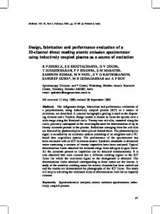
Performance Evaluation and Enhancement of 2×2 Ti: LiNbO3 Mach Zehnder Interferometer Switch at 1.3 µm and 1.55 µm Nazmi A. Mohammed*, Huda S. Abo Elnasr* and Moustafa H. Aly an OSA Member Department of Electronics and Communication, Faculty of Engineering Arab Academy for Science, Technology and Maritime Transport, Egypt Abstract: In this paper, the electro-optic 2×2 switching devices using titanium (Ti) diffused lithium niobate (Ti:LiNbO3) as a waveguide medium in the optical switch is designed based on integrated Mach-Zehnder interferometer (MZI) at 1.3 µm and 1.55 µm. Two major design parameters; insertion loss and extinction ratio are evaluated and tested in details. The novelty of this paper is obtaining the optimum, Ti, strip thickness on MZI switch that results in improving switching performance at 1.3 µm and 1.55 µm. We have optimized the switch design parameters in order to reduce the overall switch losses (≤ 0.0138 dB) and to achieve the best possible extinction ratio (= 30 dB). The designed switch has a very high switching capability and a high degree of reliability.
Keywords: Mach-Zehnder interferometer, Electro-optics, Directional couplers, Insertion loss, Extinction ratio, Lithium niobate, Planar lightwave circuit (PLC), Titanium. 1. INTRODUCTION Wavelength Division Multiplexing optical switching network (also referred to as WDM cross-connect or WXC) provides interconnections between a group of input fiber links and a group of output fiber links with each fiber link carrying multiple wavelength channels [1]. Such an optical switching network can be used to serve as an optical crossconnect (OXC) in a wide-area communication network or to provide high-speed interconnections among a group of processors in a parallel and distributed computing system [2]. Large OXC switch fabrics can be constructed using 2×2 switches arranged in a multi-stage interconnection network, such as a Banyan network (a good candidate for further use in higher order switches) [3]. A 2×2 switch is a 2×2 directional coupler which can direct the optical signal on any input to any output [4]. For switching operation, some of mechanisms, such as thermo-optic and electro-optic [5, 6] can be used. But, in optical communications, all-optical devices realizing high performance and speed are preferred. For applying the directional coupler to all- optical purposes, materials with high nonlinear characteristics are suitable [5, 6]. One of the major advantages of all-optical switches is that they avoid the need for optic-electronic and electronic-optic (o-e-o) conversions to keep data in the optical domain. [7]. In spite of the mentioned subjects, an electro-optic switch based on integrated Mach Zehnder interferometer (MZI) is required in many optical switching systems. In recent years, *Address correspondence to these authors at the Department of Electronics and Communication, Faculty of Engineering Arab Academy for Science, Technology and Maritime Transport, Egypt; Tel: +2-01006515131; Fax: +2-01143353528; E-mails:
[email protected];
[email protected] 1874-1290/12
various materials and configurations have been employed for the development of MZI optical switches [8]. In [9], a 2×2 Si waveguide with a ferro-electric liquid crystal cladding based on MZI switch is designed with 15 dB extinction ratio at 1.55 µm biased at ±30 V.Shaochun Cao et al. [10] investigated a 2×2 optical MZI switch fabricated by GaAs GaAlAs with 2 dB insertion loss and 20 dB extinction ratio at 1.55 µm. In [11] 1×4 MZI switch based on hybrid configuration of silica-based planar lightwave circuit ( PLC) and lithium niobate is explored with insertion loss of 4.2 dB and extinction ratio of 17 dB at 1.53 µm. Noriaki Koyama et al. [12] examined a 4×4 InAlGaAs/InAlAs MZI switch based on 2×2 structure with low polarization dependent loss and -20 dB crosstalk. Titanium diffused lithium niobate based on MZI switches have the following distinct advantages over previously mentioned switches with mentioned fabricated materials: 1) compatible with large capacity and long-haul optical transmission systems operating above 40 Gbit/s [13], 2) lower complexity, and 3) their large electro-optic coefficient results in a small transition time. However, titanium diffused lithium niobate based on MZI switches have inherent drawbacks like cost of higher driving voltage, polarization dependent losses and crosstalk (to achieve full switching operation) compared with previously mentioned switches with mentioned fabricated materials [14]. In our work we will investigate basic (without adaptive structure) a2×2 titanium diffused lithium niobate switch with two inexperienced contributions: 1) Performance evaluation for the switching operation of convention 2×2 titanium diffused lithium niobate switch at 1.3 µm (deigned in [3, 14]) but with novel design parameters: insertion loss, extinction ratio and studying the effect of Ti strip thickness. 2012 Bentham Open
Performance Evaluation and Enhancement of 2×2 Ti
The Open Electrical & Electronic Engineering Journal, 2012, Volume 6
37
Electrodes A1
A0
In1 In2 Fig. (1). MZI switch model.
-3dB Coupler
B1
f
2) A 2×2 titanium diffused lithium niobate switch operating at 1.55 µm will be investigated. We will introduce, for the first time, the following design parameters at 1.55 µm: electric field, power overlap integral, power in output waveguide and the previously three designed parameter mentioned in 1. The remainder of the paper is organized as follows. In Section 2, we consider the basic mathematical and idea of operation of MZI switch. In Section 3, we will introduce the design and simulation results. Finally, in Section 4, main conclusions are summarized.
A2
A3
B2
B3
-3dB Coupler
B1 = ! jA0 sin ( kl ) = ! j
OUT1 OUT2
A0 2
(6)
where ℓ is the coupling length. After passing through the interferometer straight arms, A2 and B2 (see Fig. 1) will become [15]
A2 = A1 exp ( ! j " L ) =
A0 exp ( ! j " L ) 2
B2 = B1 exp ( ! j " L + j# ) = ! j
A0 exp ( ! j " L + j# ) 2
(7) (8)
2. BASIC MATHEMATICAL MODEL AND IDEA OF MZI SWITCHING OPERATION
L denotes the length of switching region and ! donates an excess phase shift at the lower arm.
The basic (without adaptive structure) MZI switch cycles between the cross state, where most of the light appears in the waveguide on the same side as the input, and the bar state, where most the light moves to the waveguide on the other side [13].
Here, we assume that, the second coupler is also a 3-dB one having kℓ=π/4. So, the optical intensity in each output port is given by [15]
Fig. (1) represents the basic 2×2 MZI switch, where the electric field at (In1) is represented by A(Z) and the electric field at (In 2) is represented by B(Z), where A(z) and B(z)are given by [15] *" ! k % A(Z ) = + $ cos(qz) + j sin(qz) ' ( A(0) ) j k sin(qz)B(0) . ( exp() j! z) q q & ,# /
(1)
) k , " # & B(Z ) = *! j sin ( qz ) .A ( 0 ) + % cos ( qz ) ! j sin ( qz ) ( ..B ( 0 ) - .exp ( j" z ) q $ ' + q .
(2)
where q is an integer that represents the number of local electric field peaks along the x- and y-axis directions.
q = k2 + ! 2
(3)
and
% l # l2 ( ! = 2" ' 1 & $ *)
(4)
ℓ1 denotes the coupling length of the upper waveguide, ℓ2 denotes the coupling length of the lower waveguide and k donates the wave number. We consider the case in which light is coupled into the upper waveguide of a MZI. Here, we assume that both arms have the same waveguide structures; i.e., we have δ=0 which leads to A(0)=A0 and B(0)=0. When the first coupler is a 3dB coupler with kℓ=π/4, the light splitting ratios will be [15]
A1 = A0 cos ( kl ) =
A0 2
(5)
2 2 #"& A3 = A0 ! sin 2 % ( $ 2' 2 2 #"& B3 = A0 ! cos 2 % ( $ 2'
(9) (10)
The impact of changing the voltage is enforcing to the electrodes, creating an electric field distribution within the substrate, which consequently changes its refractive index [15]. When the applied voltage is 0 V which is corresponding to ! = 0, the output intensity will be switched totally to the lower port │B3│2 ≈│A0│2. At an applied certain voltage which is corresponding to ! =π depending on the nonlinear behavior of waveguide, the output intensity will be switched totally to the upper port│A3│2 ≈│A0│2.The full reflection or transmission of light is applied only in a theoretical model of 2×2 MZI switch [15]. But, in the real simulated model, there will be an insertion loss and an extinction ratio. Insertion loss of a switch is a part of power that is lost and has to be low for good performance and the extinction ratio is the ratio of output power in ON state to output power in OFF state which ideally must be very high [14]. Insertion loss and extinction ratio for each port, that are the important parameters for optical switching are given by [14, 17]
!P $ I.L ( dB ) = 10 log10 # out & " Pin %
(11)
!P $ Ex.R. ( dB ) = 10 log10 # on & " Poff %
(12)
38 The Open Electrical & Electronic Engineering Journal, 2012, Volume 6
Mohammed et al. 1.0069
0.8811
0.7552
0.6293
0.5035
0.3776
0.2517
0.1259
0.0000
Fig. (2). Optical field propagation in XZ slice for 0 V. 1.0069
0.8811
0.7552
0.6293
0.5035
0.3776
0.2517
0.1259
0.0000
Fig. (3). Optical field propagation in XZ slice for 7.2 V.
3. DESIGN AND SIMULATION RESULTS 3.1. Introduction Section 3.2 represents the common electro-optic coefficients, material and waveguide properties for all experiments. In Section 3.3, a performance evaluation for switching operation for basic Ti: LiNbO3 2×2 switch operating at 1.3 µm is presented. Section 3.4 explores the effect of titanium strip thickness on the performance of Ti:LiNbO3 2×2 switch operating at 1.3 µm. Finally, Section 3.5 represents a full investigation for the switching behavior for basic Ti:LiNbO3 2x2 MZI switch that operates at 1.55 µm. 3.2.Common Electro-optic Coefficients, Material and Waveguide Properties For All Experiments Titanium diffused lithium niobate waveguide is used as the waveguide medium in the optical switch design. The wafer is a planar substrate. Its length is along Z-axis, horizontal on the
screen and width is along X-axis, vertical on the screen. The thickness of the substrate is in y-direction, perpendicular to the screen and is not shown on the layout interface. An example of that is showed in Figs (2, 3, 7, 8, 14 and 15). The MZI switch is created on a z-cut wafer of lithium niobate and is surrounded by air cladding. The following Tables 1, 2 and 3 represent the electro-optic coefficients, material and waveguide properties which must be defined to simulate MZI switch at both 1.3 µm and 1.55 µm as in [3, 14]. After the input plane has been defined, the global data is set with a refractive index Modal Solver [3, 14]. The 2D properties have been set with TM polarization and 500 mesh points as Paraxial BPM solver, a Finite Difference engine is used. Finite difference Taylor series expansions are used to derive finite-difference schemes to approximate the wave equations. BPM 2D provides Transparent Boundary Conditions (TBC) method to escape unwanted reflections from the boundaries [3, 14].
Performance Evaluation and Enhancement of 2×2 Ti
The Open Electrical & Electronic Engineering Journal, 2012, Volume 6 Power in Output Wave Guides
1
OUT1
0.2
0.4
Power
0.6
0.8
OUT2
OUT1 0
OUT2
1
3
5
7
Iteration
9
Fig. (4). Power in output Waveguides.
In1
0.2
0.4
Power
0.6
0.8
1
Power Overlap Integral
0
OUT1
0
10000
Distance
20000
30000
Fig. (5). Power overlap integral for 0 V.
In1
OUT1
0
0.2
0.4
Power
0.6
0.8
1
Power Overlap Integral
0
Fig. (6). Power overlap integral for 7.2 V.
10000
Distance
20000
30000
39
40 The Open Electrical & Electronic Engineering Journal, 2012, Volume 6
Mohammed et al. 1.0097
0.8835
0.7573
0.6311
0.5049
0.3786
0.2524
0.1262
0.0000
Fig. (7). Optical field propagation in XZ slice for 0 V. 1.0097
0.8835
0.7573
0.6311
0.5049
0.3786
0.2524
0.1262
0.0000
Fig. (8). Optical field propagation in XZ slice for 7.2 V.
OUT2
OUT1
OUT1
OUT2
0
0.2
0.4
Power 0.6
0.8
1
Power in Output Wave Guides
1
Fig. (9). Power in output waveguides.
3
5
Iteration
7
9
Performance Evaluation and Enhancement of 2×2 Ti
The Open Electrical & Electronic Engineering Journal, 2012, Volume 6
In1
0.2
0.4
Power
0.6
0.8
1
Power Overlap Integral
0
OUT1 0
Distance
10000
30000
Power Overlap Integral
OUT1
In1
0
0.2
0.4
Power
0.6
0.8
1
Fig. (10). Power overlap integral for 0 V.
20000
0
10000
Distance
Fig. (11). Power overlap integral for 7.2 V.
20000
Field / Neff
OUT1
0
0.2
2.139
0.4
N eff
E field
2.14
0.6
0.8
2.141
1
OUT2
30000
-50
-50
Fig. (12). Electric field at 0 V.
-30
-30
-1010
Width [mm]
1010
30
30
50
50
41
42 The Open Electrical & Electronic Engineering Journal, 2012, Volume 6
Mohammed et al.
Field / Neff
OUT1
0
0.2
2.139
0.4
N eff
E field
2.14
0.6
0.8
2.141
1
OUT2
-50
-50
-30
-30
-1010
1010
30
30
50
Width [mm]
Fig. (13). Electric field at 8 V. 1.0111
0.8847
0.7583
0.6319
0.5055
0.3791
0.2528
0.1264
0.0000
Fig. (14). Optical field propagation in XZ slice for 0 V. 1.0111
0.8847
0.7583
0.6319
0.5055
0.3791
0.2528
0.1264
0.0000
Fig. (15). Optical field propagation in XZ slice for 8 V.
50
Performance Evaluation and Enhancement of 2×2 Ti
The Open Electrical & Electronic Engineering Journal, 2012, Volume 6
43
Table 1. LiNbO3 Parameter Crystal Name
LiNbO3 Electro-optic Coefficients 10¯¹²(m/V):
r33
30.8
r13
8.6
r51
28
r22
3.5
Width (µm)
Wafer Profile
8.0
Ti LiNbO3
Table 2. Material Properties Wafer Dimensions (µm) breadth
Length
100
33000 2D Wafer Properties Wafer Refractive Index: lithium niobate 3 D Wafer Properties Subtrate
Cladding
Thickness(µm)
Material
Thickness(µm)
Material
10
LiNbO3
2.0
Air
Table 3. Waveguide Properties Dielectric Material
Diffused Material
Refractive Index
Material
Propagation Direction
Crystal Cut
Crystal Name
1
Air
Y
Z
LiNbO3
Diffused Profile Ti LiNbO3
Table 4. Titanium Strip Specifications 0.05 µm
Strip Thickness Before Diffusion
5.67e+022 per cm³
Dopant constant
3.5 µm
Dv
We performed 2D isotropic calculation by using a scripting language for 1.3 µm as follows. This language is used in OptiBPM 9.0 to identify the simulation method required to obtain the switching operation for the design. Scripting: (using VB script) Const NumIterations = 10 ParamMgr.SetParam “V2”, 0.0 For x= 1 to NumIterations Param Mgr. Simulate Param Mgr. Set Param “V2”, 0.8* x WGMgr.Sleep (50) Next This script identifies number of iterations corresponding to step voltage in simulation. Then a set of commands for ordering a start of simulation, linking steps with the electrode and ending the program is presented. There is a direct relation between the number of iterations (corresponding to the step increase in the applied volt-
4.0 µm
Dh
age of electrodes i.e. 0.8 V for each iteration in the following simulations) and the switching behavior. This behavior is analyzed initially from iteration 1 with 0 V to final iteration until the switch provides a best observable switching operation. This operation depends on the operating wavelength, material and dimension (size) of the switch [16]. To create channel waveguides of titanium diffused lithium niobate, a titanium strip of a definite thickness is placed on the substrate and is heated for few hours at a temperature ranging from hundreds to few thousand degrees Celsius so that the titanium diffuses into the host lithium niobate. The resultant change in the refractive index is a function of parameters like titanium strip thickness, lateral diffusion length (Dh), vertical diffusion length (Dv), and other process parameters [3, 14]. 3.3. Simulation For Basic Ti:LiNbO3 2×2 Switch Operating at 1.3µm For this experiment, the titanium strip specifications are defined in Table 4 as in [3, 14]. The simulation for 2D isotropic calculation with the previous specifications will provide the following results (Figs. 2-6):
44 The Open Electrical & Electronic Engineering Journal, 2012, Volume 6
Mohammed et al.
Table 5. Comparison Between MZI Switches in both their Insertion Loss and Extinction Ratio Thickness Width (µm)
Switching Voltage (V) 0
0.048 7.2
0 0.05 7.2
0 0.0525 7.2
0 0.055 7.2
0 0.062 6.4
In / Out Ports (mW) In 1
1
Out 1
0.310114
Out 2
0.676059
In 1
1
Out 1
0.96927
Out 2
0.0181763
In 1
1
Out 1
0.126739
Out 2
0.861148
In 1
1
Out 1
0.979251
Out 2
0.00876452
In 1
1
Out 1
0.0101976
Out 2
0.977295
In 1
1
Out 1
0.987682
Out 2
0.00111463
In 1
1
Out 1
0.005898
Out2
0.989002
In 1
1
Out 1
0.995005
Out 2
0.00099521
In 1
1
Out 1
0.266379
Out 2
0.724723
In 1
1
Out 1
0.993998
Out 2
0.001002
Figs. (2 and 3) represent a 2D isotropic optical field distribution for XZ cut for the designed switch. In Fig. (2), the MZI switch is represented in its cross state at 0 V and in its bar state for the best observed switching operation with 7.2 V at Fig. (3). This result shows a fair agreement with the previously published literature at same wavelength and design parameter as in [3, 14]. Optical field overlap versus the number of iterations is shown in Fig. (4). This graph provides a valuable information on the following: 1) the trace of output power for distinct iteration for OUT1 and OUT2 and 2) the data required to evaluate the losses within the wave guiding structure of the switch (mainly the insertion loss). An ideal representation for this graph should be a unity value for power at OUT2 and a value of 0 at OUT1 in first iteration (when no voltage is applied). While at the final iteration, the whole input light must be fully switched to OUT1 to get a unity power at this port and no power at OUT2.
Insertion Loss (dB)
Extinction Ratio (dB)
1.7
Out2 15.7
0.136
Out1 4.9
0.649
Out2 19.9
0.09
Out1 8.88
0.0997
Out2 29.4
0.053
Out1 19.9
0.048
0ut2 30
0.022
Out1 22.3
1.398
0ut2 28.6
0.026
0ut1 5.72
Fig. (4) practically provides a best switching operation after 10 iterations (7.2 V). For iteration1 (0 V), OUT2 provides only a power of 0.861148 mW and a power of 0.126739 mW is provided by OUT1. When light is switched after 10 iterations, the output power at OUT1 is 0.979251 mW and 0.00876452 mW at OUT2 (Noting that these results are part of those which will be discussed with wider ranges in the following section-in Table 5). Remembering that, results in Sec.3.3 was done by using same values and design parameters of [3, 14] to provide ability to compare. However, the following three design parameters are not investigated in details in previous published literatures. They are insertion loss, extinction ratio and the effect of titanium strip thickness. In the following, the insertion loss and extinction ratio will be studied under the same parameters of [3, 14]. Results will show a server performance relating to insertion loss and extinction ratio under these parameters.
Performance Evaluation and Enhancement of 2×2 Ti
The Open Electrical & Electronic Engineering Journal, 2012, Volume 6
45
Table 6 Titanium Strip Specification
Dh
Strip Thickness Before Diffusion
0.0825 µm
Dopant Constant
5.67e+022 per cm³ 4.0 µm
According to Sec. 2, Eq. (11) and Fig. (6) the insertion loss is calculated to be 0.649 dB at OUT2 and to be 0.09 dB at OUT1. Secondly, the extinction ratio is represented in Figs. (5 and 6). Both figures contain the power overlap integral versus distance of propagation of waveguide for the first iteration and the final iteration, respectively. At iteration 1 in Fig. (4), the power distribution along the effective distance of switch, especially at its end, shows undesired considerable value for output power at the output of linear OUT1 waveguide which has to be 0 in ideal MZI switching performance. While, in Fig. (5) at iteration 10 (when its fully switched at 7.2 V), the distribution of power along the waveguide experienced a significant losses at its boundaries especially at the end of linear OUT1 waveguide. These losses lead to a severe decrease in output power preventing it to be unity (the default is to be unity for ideal performance). This results in an undemanding decrease in the extinction ratio to be 8.88 dB for OUT1 port and 19.9 dB for the other port. From the previous results, it is clear that extinction ratio and insertion loss are major drawbacks for titanium diffused lithium niobate switches under the previous parameters. Previous literature suggested that, these two drawbacks can be enhanced by controlling titanium strip thickness before diffusion [18]. This will be investigated in the following section. 3.4. Exploring the Effect of Titanium Strip Thickness on the Performance of Ti:LiNbO3 2×2 Switch Operating at 1.3 µm In this section, we are going to investigate the effect of titanium strip thickness on for titanium diffused lithium niobate switch using a sample of suggested range from 0.048 µm to 0.062 µm in [18]. Table 5 represents the results of studying important design parameters under the samples of suggested Ti strip thickness range. A remarkable performance (insertion loss and extinction ratio) is observed for the switch at 0.055 µm for titanium strip thickness compared to that in [3, 14] and in Sec. 3.3. Figs. (7-11) show the simulation for 2D isotropic calculation for the proposed switch with 0.055 µm for titanium strip thickness that provided a remarkable performance throughout the simulation. According to the results, we obtain a low insertion loss of 0.048 dB for OUT2 and 0.022 dB for OUT1 is achieved. While, high extinction ratio of 30 dB for OUT2 and 22.3 dB for OUT1 are obtained with maintaining same switching voltage. These results can be understood when 1st: indicating that the resultant change in the refractive index (that effect the switching operation and hence the losses levels) is a function of parameters like Ti-strip thickness, lateral diffusion length
Dv
3.4 µm
(Dh), vertical diffusion length (Dv), and other process parameters [16, 18]. The ranges of Ti-strip thickness (as in Table 5) have been selected because in these ranges the Ti atoms cause sufficient changes in the refractive index of lithium niobate substrate, needed for the switch to remain in the bar state for zero voltage and cross state for 7.2 voltage for the switching operation described before. This shows fair agreement with basic switching operation of Ti-LiNBO3 S-bend switch in [18] Little increment in Ti-strip thickness, provisioning of concentrated optical power through the channel waveguides enhances, which results in reduction of insertion losses of the switch as indicated clearly in Table 5 till reaching the optimum thickness then a reverse characteristic is observed. We think after exceeding the optimum thickness some power radiates resulting on small increase in the insertion losses. Based on the definition of extinction ratio provided in section 2 Eq.12, at higher values of Ti-strip thickness, extinction ratio can be maintained comparatively at higher levels. We think this is because increasing the thickness of the strip results in more power confinement in the switch waveguide, which results in low coupling losses, thereby reducing the possibility of power leakage to undesired path and higher extinction values till reaching the optimum strip thickness. 3.5. Simulation for Basic Ti: LiNbO3 2×2 MZI Switch Operating at 1.55 µm 3.5.1. Introduction, Modified Specification and VB Scripting To the best of our knowledge it will be the first time to fully investigate a 2×2 titanium diffused lithium niobate switch operating at 1.55 µm. The novelty of this work is based on optimizing the thickness of titanium strip (for basic 2×2 switch) to successfully switch a light of 1.55 µm to targeted output. To approach this target, we applied a certain range (0.0725 µm – 0.09 µm) for the titanium strip thickness before diffusion [18]. We finally reached to optimum strip thickness which gives the least possible losses especially for insertion loss and highest possible extinction ratio. We will also introduce the following design parameters that evaluate the switching performance: Electric field, Power overlap integral, Power in output waveguide at 1.55 µm. For this experiment, the titanium strip specifications are defined in Table 6. A 2D isotropic calculation is performed using the following VB script in OptiBPM 9.0 but with slightly increasing in range of voltage (8 V required to switch the light successfully). Scripting: (using VB script) Const NumIterations = 10 ParamMgr.SetParam “V2”, 0.0
46 The Open Electrical & Electronic Engineering Journal, 2012, Volume 6
Mohammed et al.
Table 7. Comparison between MZI Switches in both their Insertion Loss and Extinction Loss Thickness Width (µm)
Switching Voltage (V) 0
0.0725 8.8
0 0.0775 8.8
0 0.08 8.8
0 0.0825 8
0 0.085 8
0 0.0875 8
0 0.09 8
In / Out Ports (mW) In 1
1
Out 1
0.400972
Out 2
0.587884
In 1
1
Out 1
0.987971
Out 2
0.002018
In 1
1
Out 1
0.903844
Out2
0.085898
In 1
1
Out 1
0.989355
Out 2
0.000945
In1
1
Out1
0.0152184
Out2
0.973531
In1
1
Out1
0.994428
Out2
0.0020552
In 1
1
Out 1
0.0010134
Out 2
0.996823
In 1
1
Out 1
0.997042
Out 2
0.00099879
In1
1
Out1
0.0161005
Out2
0.972719
In1
1
Out1
0.992989
Out2
0.001774
In1
1
Out1
0.0680115
Out2
0.92171
In1
1
Out1
0.992262
Out2
0.001811
In1
1
Out1
0.134775
Out2
0.854289
In1
1
Out1
0.991077
Out2
0.00195232
Insertion Loss (dB)
Extinction Loss (dB)
2.3
Out2 24.6
0.053
0.439
0.046
Out1 3.9 0ut2 29.8
Out1 10.6 0ut2
0.117 26.8
0.024
Out1 18.2
0.0138
Out2 30
0.0129
Out1 29.9
0.12
Out2 27.4
0.0306
Out1 17.9
0.354
Out2 27
0.034
Out1 11.6
0.68
Out2 26.4
0.039
Out1 8.67
For x= 1 to NumIterations
3.5.2 Results and Discussion
ParamMgr.Simulate
In Table 7, we repeated the previous analysis of Sec. 3.4 to discover the optimum titanium strip thickness that leads to the following unique switching capability with acceptable insertion loss and extinction ratio. A range from 0.0725µm – 0.09µm [18] is tested as follows.
ParamMgr.SetParam “V2”, 0.8* x WGMgr.Sleep (50) Next
Performance Evaluation and Enhancement of 2×2 Ti
The Open Electrical & Electronic Engineering Journal, 2012, Volume 6
47
OUT1
OUT2
0.2
0.4
Power
0.6
0.8
1
Power in Output Wave Guides
OUT2
0
OUT1 1
3
5
Iteration
7
9
11
Fig. (16). Power in output Waveguide.
In1
0.2
0.4
Power
0.6
0.8
1
Power Overlap Integral
0
OUT1 0
10000
Distance
20000
30000
Fig. (17). Power overlap integral for 0 V.
From the table, the optimum titanium strip thickness is 0.825 µm. This will be verified clearly in the following discussions. In the following Fig. (12-18), we represent a performance evaluation for the switch's important design parameters (as in Sec. 3.3) at 1.55 µm with the optimum chosen titanium strip thickness of 0.825 µm. Figs. (12 and 13) represent the electric field for both OUT1 and OUT2 at first iteration and final iteration, respectively. The ideal operation is represented by the red graph, while the blue one represents the operation of the proposed switch. In Fig. (14) MZI switch is represented in its cross state at 0 V and in its bar state for the best observed switching opera-
tion with 8 V at Fig. (15). It is observed that, full switching behavior at 1.55 µm requires a more switching voltage (8 V) than 1.3 µm (7.2V). The analytical result in Fig. (16) provides the best inexperienced switching capability but after 11 iterations (8 V). Iteration1 (0V), provides a power of 0.996823 mW at OUT2 and only a power of 0.0010134 mW is provided by OUT1. While, for iteration 11 (8 V), the light is fully switched to target OUT1 to output power of 0.997042 mW and only a power of 0.00099879 mW at OUT2. This leads an insertion loss of 0.0138 dB for OUT2 and 0.0129 dB for OUT1. Comparing this result with previous results for switches operating
48 The Open Electrical & Electronic Engineering Journal, 2012, Volume 6
Mohammed et al.
In1
OUT1
0
0.2
0.4
Power
0.6
0.8
1
Power Overlap Integral
0
10000
20000
Distance
30000
Fig. (18). Power overlap integral for 8 V.
at 1.55 µm in Table 7 and for other ones operating at 1.3 µm in Sec. 3.4, a better switching performance is observed. Figs. (17 and 18) contain the power overlap integral versus distance of propagation of waveguide for the first iteration and the final iteration, respectively. The high extinction ratio of 30 dB for OUT2 and 29.9 dB for OUT1 are obtained. By comparing this ratio with other previous ratios for switches operating at 1.55 µm in Table 7 and also for other ones operating at 1.3 µm in Sec. 3.4, the best performance with higher ratio is achieved. Switch operation at 1.55 µm (this section) provides similar behavior to the switch operation at 1.3 µm but with better performance. This is clear when observing the behavior of insertion loss and extinction ratio. When viewing insertion loss we found a common decrease in the insertion loss with increasing Ti strip thickness until reaching optimum value of thickness then the behavior is reversed. Reasons for such behavior stated clearly in section 3.4 (under Fig. 11). Noting that level of insertion loss at both output ports at 1.55 µm are lower than the case of 1.3 µm switching operation. Other similarity in behavior can be observed for extinction ratio, it increases with increasing Ti strip thickness until reaching optimum value of thickness then the behavior is reversed. This indicates that beyond the optimum thickness lower power confinement results in decreasing the extinction ratio. More details can be found in end of section 3.4 In 1.55 µm from Table 7 we observe at optimum case we need 8 volt (11 iterations) to make full switching operation with the mentioned remarkable low insertion loss and high extinction ratio. In 1.3 µm we notice that we need slightly lower voltage (7.2 volt -10 iterations) to get its optimum performance values which generally worse than that observed from 1.55 µm switching operation.
optical signal at both wavelengths 1.3 µm and 1.55 µm. An optimum titanium strip thickness is tested and performance evaluation is performed. Insertion loss and extinction ratio show a performance enhancement at 1.55 µm with an optimum titanium strip thickness of 0.0825 µm but with a higher driving voltage (8 V) compared to that of 1.3 µm (7.2 V) operation. The simulated insertion loss is 0.0138 dB for OUT2 and 0.0129 dB for OUT1 with extinction loss of 30 dB for OUT2 and 29.9 dB for OUT1 at 1.55 µm these values are better than that for 1.33 µm optimum switching case. A comparative study on the effect of titanium strip thickness on the switching capability at 1.3 µm shows a remarkable improvement in reduction of insertion loss to be 0.048 dB for OUT2 and 0.022 dB for OUT1 for the optimum thickness. Also, a high extinction ratio of 30 dB for OUT2 and 22.3 dB for OUT1 is achieved. These results are better than those observed from previous literatures [13, 14] dealing with the same structure and design parameters but we get the previous better performance with optimizing the Ti-strip thickness. Noting that all these results still lower than that observed for 1.55 µm cases in the price of increasing the electrode voltage. CONFLICT OF INTEREST The authors confirm that this article content has no conflicts of interest. ACKNOWLEDGEMENT Declared none. REFERENCES [1]
4. CONCLUSION An optimum 2×2 MZI optical switch based on electroopto effects has been successfully designed for switching
[2]
Young Han Choe and Venkatesen Mauree of the ITU Telecommunication Standardization Bureau, "The Optical World," ITU Technology Watch Report, 2011. Michael J. O’Mahony, "Future Optical Networks," IEEE Journal Of Lightwave Technology, vol. 24, no. 12, pp. 4684-4696, Dec. 2006.
Performance Evaluation and Enhancement of 2×2 Ti [3] [4] [5] [6] [7] [8] [9]
[10]
[11]
The Open Electrical & Electronic Engineering Journal, 2012, Volume 6
V. Sachdeva1, "Design of 4×4 Banyan optical switch using optoelectronic MZI switches with low crosstalk," Indian Journal of Science and Technology, vol. 2, no. 10, pp. 48-51 , Oct. 2009 F. Liu, X. Zheng, "New Types of 2×2 Wavelength-Switching Blocks for Optical Cross-Connects," IEEE Photonics Technology Letters, vol. 13, no. 5, May. 2001. Georgios I. Papadimitriou, "Optical Switching: Switch Fabrics, Techniques, and Architectures," Journal of Lightwave Technology, vol. 21, no. 2, pp. 384-405, Feb. 2003. Andrzej Jajszczyk, "Optical networks—the electro-optic reality," Journal of Optical Switching and Networking, no. 1, pp. 3-18, 2005. Y. Yang, "WDM Optical Switching Networks Using Sparse Crossbars," IEEE Infocom., 2004. M. P. Earnshaw," 8×8 Optical Switch Matrix Using Generalized Mach–Zehnder Interferometers," IEEE Photonics Technology Letters, vol. 15, no. 6, pp. 810-812, 2003. T. Sasaki, "Demonstration of switching operation in a symmetric Mach-Zehnder Interferometer Switch using Si waveguide with a ferro-electric liquid Crystal Cladding," In proceedings of the IEEE Lasers and Electro-Optics Conference, Seoul, Aug. 2007, pp. 1-2. Shaochun Cao, "2×2 MMI-MZI GaAs-GaAlAs Carrier-Injection Optical Switch," In proceedings of the IEEE Society Summer Topical Meeting Series Conference, Playa del Carmen, J. 2010, pp. 207208. K. Suzuki," High-Speed Optical 1×4 Switch Based on Generalized Mach–Zehnder Interferometer With Hybrid Configuration of Sil-
Received: November 11, 2012
[12]
[13] [14]
[15] [16] [17]
[18]
49
ica-Based PLC and Lithium Niobate Phase-Shifter Array," IEEE Photonics Technology Letters, vol. 19, no. 9, pp. 674-676, May 2007. Y. Ueda,"4×4 InAlGaAs/InAlAs optical switch fabric by cascading Mach-Zehnder interferometer -type optical switches low-power and low -polarization -dependent operation," In proceedings of the 23rd International Conference Indium Phosphide and Related Materials, Berlin, Germany, 2011. G.Singh, "Ti indiffused Lithium Niobate (Ti: LiNbO3) MachZehnder interferometer all optical switches: A review," New, Advanced Technologies, pp. 312-322, 2010. G. Singh, "Design of 2×2 Optoelectronic Switch Based on MZI and Study the Effect of Electrode Switching Voltages," Journal of World Academy of Science, Engineering and Technology, vol. 39, pp. 401-407, 2008. Katsunari Okamoto, Fundamentals of Optical Waveguides, 2nd ed., Laboratory Ltd Ibaraki: Japan, 2006. OptiBPM 9.0 Technical Background and Tutorials, Waveguide Optics Modeling Software Systems, Optiwave, 2007. M. Syuhaimi A, Analytical and Simulation of New Electro-Optic 3×3 Switch Using Ti:LiNbO3 As a Wave Guide Medium," In Proc. of the IEEE Conference of Photonics, Langkawi, Kedah, J. 2010, pp. 1-5. G. Singh, " Modeling of a 2×2 electro-optic Mach–Zehnder Interferometer optical switch with s–bend arms, " Photonics Letters of Poland, vol. 3, no. 3, pp. 119-121, 2011.
Revised: November 24, 2012
Accepted: December 02, 2012
© Mohammed; Licensee Bentham Open. This is an open access article licensed under the terms of the Creative Commons Attribution Non-Commercial License (http://creativecommons.org/licenses/by-nc/3.0/) which permits unrestricted, non-commercial use, distribution and reproduction in any medium, provided the work is properly cited.