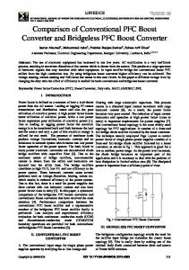
International Journal of Pure and Applied Mathematics Volume 118 No. 11 2018, 137-144 ISSN: 1311-8080 (printed version); ISSN: 1314-3395 (on-line version) url: http://www.ijpam.eu doi: 10.12732/ijpam.v118i11.17 Special Issue
ijpam.eu
QUADRATIC BOOST CONVERTER USING Π-FILTER FOR DISTRIBUTED GENERATION SYSTEM 1
Nishant S, 2Jayaramapradeep Assistant Professor, St.Joseph’s College of Engineering, Chennai, India 2 M.E., Ph.D., Associate professor, EEE Dept. St.Joseph’s College of Engineering, Chennai, India 1
[email protected]
1
Abstract: Generally implementation high volt D.C applications require a high volt A.C source. This source is then converted to D.C. The whole process includes more losses. It can be reduced by using a normal A.C supply with a boost converter. The general boost converter for obtaining high-output voltage it should operate at high duty cycle but it generates more EMI, conduction loss and increase the switch rating. In this paper novel high step-up dc converter with an improved switching method is being used. Here in this circuit, it utilizes two capacitors and one coupled inductor. The two capacitors are charged in parallel during the switch-off period and are discharged in series during the switch-on period by the energy stored in the coupled inductor to achieve a high step-up voltage gain. In addition, the leakage-inductor energy of the coupled inductor is recycled with a passive clamp circuit. Thus, improving the efficiency and the voltage stress on the main switch is reduced. The switch with low resistance RDS(ON) can be adopted to reduce the conduction loss. The power factor of the system is improved by high switching. The output side pi filter is used to improve the output and reduce the ripple voltage. 1. Introduction In recent years, distributed generation (DG) systems based on renewable energy sources have rapidly developed. The DG systems are composed of micro source like photovoltaic (PV) cells and wind power. Although PV cells can connect in series to obtain sufficient dc voltage, it is difficult to avoid the shadow effect. Thus, high step-up dc converters are usually used as the front-end converters to step from low voltage to high voltage which are required to have a large conversion ratio, high efficiency, and small volume. Theoretically, the boost converter can provide a high step-up voltage gain with an extremely high duty cycle. In practice, the step-up voltage gain is limited by the
137
effect of the power switch, rectifier diode, and the equivalent series resistance of the inductors and capacitors. Also, the extreme duty cycle operation may result in serious reverse recovery and electromagnetic interference problems. Some converters like the forward and flyback converters can adjust the turn ratio of the transformer to achieve a high step up voltage gain. However, the main switch will suffer high voltage spike and high power dissipation caused by the leakage inductor of the transformer. Although the non-dissipative snubber circuits and active-clamp circuits can be employed, the cost is increased due to the extra power switch and high side driver. To improve the conversion efficiency and achieve a high step up voltage gain, many step-up converters have been proposed. A high step-up voltage gain can be achieved by the use of the switched-capacitor and voltage-lift techniques. However, the switch will suffer high charged current and conduction loss. The converters use the coupled-inductor technique to achieve a high step-up gain. However, the leakage inductor leads to a voltage spike on the main switch and affects the conversion efficiency. For this reason, the converters using a coupled inductor with an active-clamp circuit have been proposed. An integrated boost flyback converter is presented in which the secondary side of the coupled inductor is used as a flyback converter. Thus, it can increase the voltage gain. Also, the energy of the leakage inductor is recycled to the output load directly, limiting the voltage spike on the main switch. Additionally, the voltage stress of the main switch can be adjusted by the turn ratio of the coupled inductor. To achieve a high step-up gain, it has been proposed that the secondary side of the coupled inductor can be used as flyback and forward converters. Also, several converters that combine output-voltage stacking to increase the voltage gain are proposed. Additionally, a high step-up boost converter that uses multiple coupled inductors with
International Journal of Pure and Applied Mathematics
output stacking has been proposed. To achieve high stepup voltage gain and high efficiency, this paper proposes a novel high step-up ratio and clamp-mode converter. The proposed converter adds two capacitors and two diodes on the secondary side of the coupled inductor to achieve a high step-up voltage gain. The coupled inductor can charge two capacitors in parallel and discharge in series. However, the leakage inductor of the coupled inductor may cause high power loss and a high voltage spike on the switch. Thus, a passive clamping circuit is needed to clamp the voltage level of the main switch and to recycle the energy of the leakage inductor. [1] Converters without using Transformer provide More voltage gain required at extreme duty cycle but the Diode reverse-recovery problem comes to front. Also the EMI increases. [2] Another technology based on a switched-capacitor circuit gives High power density and Better voltage regulation but the power loss is too high and hence the efficiency is very low. [3] In circuits where voltage clamp in fly back converters are applied More voltage gain, Less voltage spike due to active clamp circuit are obtained. But the cost is high due to more number of switches. Thus can’t be used where cost affects. [4] In Switched-capacitor and switched-inductor used converters with transformer less hybrid dc–dc PWM prototype. We obtain improved voltage gain and improved efficiency. The main Disadvantage is More charge current and More conduction losses. [5] In this converter where it utilizes the concept of leakage inductance, the main disadvantage is more voltage spike in inductance. [6]Voltage stress is reduced due to coupled inductor. The leakage energy is recycled in integrated boost–fly back step up converter analysis but it required bulk transformer to transfer and store energy. This circuit is used to obtain a high DC output voltage. It uses A.C input VS and uses a novel step-up converter to get the high D.C voltage. It proposes two capacitors are charged in parallel during the switch-off period and are discharged in series during the switch-on period by the energy stored in the coupled inductor to achieve a high step-up voltage gain. In addition, the leakage-inductor energy of the coupled inductor is recycled with a passive clamp circuit. Thus, improving the efficiency and the voltage stress on the main switch is reduced. The switch with low resistance can be adopted to reduce the conduction loss. The power factor of the system is improved by high switching. The output side πfilter is used to improves the output and reduce the ripple voltage.
138
Special Issue
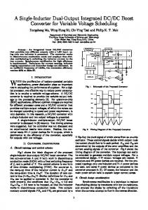
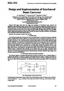
Figure.2 shows the circuit topology of the proposed converter, which is composed of dc input voltage Vin, main switch S,
Figure 1. Block Diagram of Proposed Circuit
Figure 2. Circuit Diagram of Proposed Circuit coupled inductors NP and Ns, one clamp diode D1, clamp capacitor C1, two capacitors C2 and C3, two diodes D2 and D3 output Diode D0. The output capacitor C01 and C02 with L forms π-filter which is used to reduce the ripple in the output voltage. The equivalent circuit model of the coupled inductor includes magnetizing inductor Lm, leakage inductor Lk, and an ideal transformer 2. Description The leakage inductor energy of the coupled inductor is recycled to capacitor C1, and thus, the voltage across the switch S can be clamped. The voltage stress on the switch is reduced significantly. Thus, low conducting
International Journal of Pure and Applied Mathematics
resistance RDS(ON) of the switch can be used. The original voltage-clamp circuit was first proposed in [3] “Highefficiency dc/dc converter with high voltage gain” which focuses on more voltage gain and improved efficiency to recycle the energy stored in the leakage inductor. Based on the topology, the proposed converter combines the concept of switched-capacitor and coupled-inductor techniques. The switched-capacitor technique proposes that capacitors can be parallel charged and series discharged to achieve a high step-up gain. Based on the concept, the proposed converter puts capacitors C2 and C3 on the secondary side of the coupled inductor. Thus, capacitors C2 and C3 are charged in parallel and are discharged in series by the secondary side of the coupled inductor when the switch is turned off and turned on. Because the voltage across the capacitors can be adjusted by the turn ratio, the high step-up gain can be achieved significantly. Also, the voltage stress of the switch can be reduced. Thus, the proposed converter has low conduction loss. Moreover, the secondary-side leakage inductor of the coupled inductor can alleviate the reverserecovery problem of diodes, and the loss can be reduced. In addition, the proposed converter adds capacitors C2 and C3 to achieve a high step-up gain without an additional winding stage of the coupled inductor. The coil is less than that of other coupled inductor converters. The main operating principle is that, when the switch is turned on, the coupled inductor induced voltage on the secondary side and magnetic inductor Lm is charged by Vin. The induced voltage makes Vin, VC1, VC2, and VC3 release energy to the output in series. The coupled inductor is used as a transformer in the forward converter. When the switch is turned off, the energy of magnetic inductor Lm is released via the secondary side of the coupled inductor to charge capacitors C2 and C3 in parallel. To simplify the circuit analysis, the following conditions are assumed. 1. Capacitors C1, C2 and are large enough. Thus VC1, VC2 and VC3 are considered as constants in one switching period. 2. Capacitors C01 and C02 with inductor L at output are considered large such that VC01 and VC02 provide a continuous current during switch off period. 3. The power devices are ideal, but the parasitic capacitor of the power switch is considered. 4. The coupling coefficient of the coupled inductor k is equal to Lm/(Lm + Lk), and the turn ratio of the coupled inductor n is equal to Ns/Np. 5. The proposed converter operating in continuous conduction mode (CCM) and discontinuous conduction mode (DCM) is analyzed as follows.
139
Special Issue
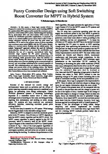
3. CCM Operation This section presents the operation principle of the proposed converter. Here VS is the source supply which is then converted to D.C using diode bridge named VIN The following analysis contains the explanation of the power flow direction of each mode. In CCM operation, there are five operating modes in one switching period. The operating modes are described as follows. A. Mode I [t0, t1] In this interval, S is turned on. Diodes D1 and D0 are off, and D2 and D3 are on. The current-flow path is shown in Fig.3(a). The leakage inductor LK starts to charge from supply Vin. Due to this, the secondary side current of the coupled inductor is decreased linearly as it discharges to the load.
International Journal of Pure and Applied Mathematics
Special Issue
current path. Diode D1, D2, and D3 are turned off and D0 is turned on. Fig.3 (c) showsthe Mode III operation. The energies of leakage inductor Lk and magnetizing inductor Lm charge the parasitic capacitor Cds of main switch S. Output capacitors provides its energy to load R. When the capacitor voltage VC1 is equal to Vs+ Vdsat t = t3, diode D1 conducts, and this operating mode ends. D. Mode IV [t3, t4] Swich S continues to be off state completely. Parasitic capacitor is also in off state Diodes D1 and D0 are turned on, and D2 and D3 are turned off. The current-flow path is shown in Fig.3 (d). The energies of leakage inductor Lk and magnetizing inductor Lm charge clamp capacitor C1. The energy of leakage inductor Lk is recycled. Current iLk decreases quickly. Secondary side voltage VL2 of the coupled inductor continues charging high-voltage output capacitors (C01 and C02) and load R in series until the secondary current of the coupled inductor is equal to zero. Meanwhile, diodes D2 and D3 start to turn on. When iDo is equal to zero at t = t4, this operating mode ends. E. Mode V [t4, t5]
Figure 3. Current-flow path of operating modes during one switching period at CCM operation. (a) Mode I. (b) Mode II. (c) Mode III. (d) Mode IV. (e) Mode V. The voltage equation on the leakage and magnetic inductors is expressed as Vin=VLk+VLm. Output capacitors provides its energy to load R..When current iD2 becomes zero at t = t1, this operating mode ends. Still the switch is in the on condition. B. Mode II [t1, t2] Switch continues to be in state at the beginning of this mode, diode D1, D2, and D3 are turned off and D0 is turned on. The current-flow path is shown in Fig.3 (b). Magnetizing inductor Lm charges in this mode and continues to deliver a part of it to the secondary of the circuit. Thus, Vin, VC1, VC2, and VC3 which are connected in series induces voltage in the secondary VL2, discharge to high-voltage output capacitors (C01 and C02) and load R. This operating mode ends when switch S is turned off. C. Mode III [t2, t3] In this mode the supply current is not circulated through the switch. The parasitic capacitor across switch allows a
140
During this time interval, S is turned off. Diode D1, D2, and D3 are turned on and D0 is turned off. The currentflow path is shown in Fig.3 (e). Output capacitors C01 and C02 are discharged to load R. Inductor Lk and magnetizing inductor Lm charge clamp capacitor C1. Magnetizing inductor Lm is released via the secondary side of the coupled inductor and charges capacitors C2 and C3. Thus, capacitors C2 and C3 are charged in parallel. As the energy of leakage inductor Lk charges capacitor C1, the current iLk decreases, and is increases gradually. This mode ends at t = t6 when S is turned on at the beginning of the next switching period. Fig.3 shows current flow path of different operating modes during one switching period at Continuous Conduction Mode(CCM) 4. Design and Experiment of the Proposed Converter To verify the performance of the proposed converter, a prototype circuit is implemented in the Simulink laboratory. The specifications are as follows: 1) Input dc voltage VIN: 25.7 V; 2) Output dc voltage Vo: 384 V; 3) Maximum output power: 179 W; 4) Switching frequency: 50 kHz; 5) Np : Ns = 1 : 4, Lm = 48 μH, and Lk = 0.25 μH; 8) Capacitors C1/C2/C3 : 22 μF/200 V, and 9) Π-filter details C01=C02=220 μF, L=0.5 μH
International Journal of Pure and Applied Mathematics
Special Issue
5. Simulink Model for Proposed Circuit
Figure 4. Circuit Diagram for Proposed Converter Table Showing the Software implementation parameter values and Output Parameters Voltage
Proposed 384 V
Current
0.475 A
Power factor
0.9942 6. Output Waveforms
Simulink model results are shown below in fig.5. Fig.5(a) Gate to source voltage is kept constant to 1V. the gate input is fed from the PIC. The fig.5(b) shows the output of the diode rectifier which is given as the input converter circuit. In Fig.7.(a) Waveforms shows the output current and fig.7.(b) shows the output voltage are shown. Current is approximately 0.45A and output voltage as 385V. The power output waveform is shown in fig.6. It is nearly 183W. Fig.8 shows the current comparison of conventional and proposed circuit. In Fig.9. shows the comparision between the voltages of conventional and proposed Circuit. The dark and upper wave shows the output of proposed waveform and light or below waveform shows for conventional circuit Fig.10 shows the comparision of power in convertional and propposed circuit. The dark plot wave shows the power of proposed circuit and lightly plotted wave shows the output of the conventional circuit.
141
Figure 5. (a)Waveforms for Gate to Source Voltage (b)The Rectified Input Supply Voltage
Figure 6. Waveforms for Output Power
International Journal of Pure and Applied Mathematics
Figure 7. Waveforms for Output Current and Output Voltage
Special Issue
Figure 10. Power Waveform Showing the Comparision Between Conventional And Proposed Circuit 7. Hardware Implementation
Figure 8. Current Waveform Showing the Comparision Between Conventional And Proposed Circuit
Figure 11. Input voltage given to the converter
Figure 9. Voltage Waveform Showing the Comparision Between Conventional And Proposed Circuit
Figure 12. Input voltage given to the Gate of the Switch
142
International Journal of Pure and Applied Mathematics
Special Issue
[3] R. J. Wai and R. Y. Duan, “High-efficiency dc/dc converter with high voltage gain,” Proc. Inst. Elect. Eng.—Elect. Power Appl., vol. 152, no. 4, pp. 793–802, Jul. 2005. [4] B. Axelrod, Y. Berkovich, and A. Ioinovici, “Switched-capacitor/ switched-inductor structures for getting transformerless hybrid dc–dc PWMconverters,” IEEE Trans. Circuits Syst. I, Reg. Papers, vol. 55, no. 2, pp. 687–696, Mar. 2008. [5] N. P. Papanikolaou and E. C. Tatakis, “Active voltage clamp in fly back converters operating in CCM mode under wide load variation,” IEEE Trans Ind. Electron., vol. 51, no. 3, pp. 632–640, Jun. 2004.
Figure 13. Output voltage across the load Results after the hardware implementation are shown above. Fig.11 show the input voltage given to the converter it is measured to be 16.4V. The input voltage given to the gate is shown the Fig.12. a 12V, 47Hz input frequency is given as the Gate-Source voltage. The final output of 149.7 volt is obtained across the load connected to the circuit. Fig.13 show the output voltage. 8. Conclusion This paper has proposed a novel high step-up dc converter for Distributed Generation systems. By using the capacitor charged in parallel and discharged in series by the coupled inductor, high step-up voltage gain and high efficiency are achieved. The steady state analyses have been discussed in detail. The converter has been simulated successfully and can be implemented with the results obtained. The use of π-filter reduced the ripple in voltage and current. Also the other parameters like power factor have been improved from 0.992 to 0.995. The experimental results have confirmed that high efficiency and high step-up voltage gain can be achieved. Additionally, the voltage on the main switch is clamped at 88 V; thus, a switch with e resistance RDS(ON) can be selected. References [1] Yi-Ping Hsieh, Jiann-Fuh Chen “Novel High StepUp DC–DC Converter for Distributed Generation System “IEEE transactions on industrial electronics, vol. 60, no. 4, april 2013 [2] K. C. Tseng and T. J. Liang, “Analysis of integrated boost–fly back step up converter,” Proc. Inst. Elect. Eng.—Elect. Power Appl., vol. 152, no. 2, pp. 217–225, Mar. 2005.
143
[6] L. S. Yang, T. J. Liang, and J. F. Chen, “Transformer-less dc–dc converter with high voltage gain,” IEEE Trans. Ind. Electron., vol. 56, no. 8, pp. 3144–3152, Aug. 2009. [7] S. Park, Y. Park, S. Choi,W. Choi, and K. Lee, “Soft-switched interleaved boost converters for high stepup and high power applications,” IEEE Trans. Power Electron., vol. 26, no. 10, pp. 2906–2914, Oct. 2011. [8] L. Huber and M. M. Jovanovic, are proposed “A design approach for server power supplies for networking,” in Proc. IEEE INTELEC 2000, pp. 1163– 1169. [9] S.V.Manikanthan and D.Sugandhi “ Interference Alignment Techniques For Mimo Multicell Based On Relay Interference Broadcast Channel ” International Journal of Emerging Technology in Computer Science & Electronics (IJETCSE) ISSN: 0976-1353 Volume- 7 ,Issue 1 –MARCH 2014. [10] T. Padmapriya, V.Saminadan, “Performance Improvement in long term Evolution-advanced network using multiple imput multiple output technique”, Journal of Advanced Research in Dynamical and Control Systems, Vol. 9, Sp-6, pp: 990-1010, 2017. [11] Rajesh, M., and J. M. Gnanasekar. "Path observation-based physical routing protocol for wireless ad hoc networks." International Journal of Wireless and Mobile Computing 11.3 (2016): 244-257. [12] Mohamed Arif.N, Y.udhayakumar, Inbarasan.G, “Design of High Frequency Earthing System Used for Gas Insulated Substation”, International Innovative Research Journal of Engineering and Technology, ISSN NO: 2456-1983. Volume 2, Issue 1 September (2016) 37-43.
144