Connecting TCAD To Tapeout
A Journal for Process and Device Engineers
Simulation and Characterization of High-Frequency Performances of Advanced MIM Capacitors J.Piquet(1), O.Cueto(2), F.Charlet(3), M.Thomas(4), C.Bermond(1), A.Farcy(4), J. Torres(4), B.Fléchet(1) (1) LAHC, Université de Savoie, Bâtiment Le Chablais, 73376 Le Bourget du lac cedex, France. (2) CEA/DRT-LETI/D2NT-CEA/GRE, 17 rue des Martyrs, 38054 Grenoble Cedex 9, France. (3) SILVACO. 55 rue Blaise Pascal 38330 Montbonnot St Martin France. (4) STMicroelectronics, 850 rue Jean Monnet, 38926 Crolles cedex, France
[email protected],
[email protected],
[email protected],
[email protected]
Abstract: High-frequency simulations and characterizations of advanced metal-insulator-metal (MIM) capacitors with ultra thin 32 nm PECVD Si3N4 dielectric are presented. The frequency dependent behavior of capacitors is numerically and experimentally extracted over a wide frequency bandwidth. Numerical results are validated by comparison to experimental results. An equivalent circuit model of capacitors including four parameters is developed for a better understanding of the frequency dependent behavior. We focused on the impact of design on the performances of MIM capacitors realized on Si substrates.
(metal5) and M6 (metal6) levels. Such MIM capacitors have been integrated among multilevel copper interconnects in a 120 nm technology node, using Si3N4 to reach 2 fF/µm2 capacitances. Special attention is paid on high-frequency performances as RF and analog applications are targeted. A new 3D electromagnetic simulator (QUEST) is used to predict electrical performances of MIM capacitors. High frequency characterizations coupled with QUEST results are carried out to evaluate the impact of both the introduction of copper and the design of electrodes on performances.
2. Simulation and Characterization
1. Introduction
The goal of this paper is to present a complete methodology to analyze and predict MIM capacitors performances built on a reliable and efficient 3D simulation tool validated by comparison with measurements. An electrical model of MIM capacitors is extracted from scattering parameters to obtain a better understanding of the frequency behavior of the capacitors.
The Metal-Insulator-Metal capacitor is a key passive component in Radio Frequency (RF) and analog integrated circuits. MIM capacitors have attracted great attention because of their high capacitance density that supplies small area, increases circuit density, and further reduces the fabrication cost. They provide good voltage linearity properties. Developments focus on capacitance density increase through the introduction of high-k materials to replace Si3N4 (k ~ 7) and 3D high-density architectures.
Continued on page 2 ...
The improvement of performances thanks to Cu introduction in interconnects naturally leads to the integration of copper as a metal electrode for MIM capacitors. The objective is to improve the quality factor by reducing parasitic resistances and ensure the compatibility of MIM capacitor integration scheme with copper interconnect one. The required damascene architecture was first presented for TiN/Si3N4/TiN MIM capacitors [1]. Here, a Cu/Si3N4/TaN/Cu stack is implemented between M5 Volume 15, Number 11, November 2005 November 2005
INSIDE Numerical Analysis of GaInP Solar Cells: Toward Advanced Photovoltaic Devices Modeling............ 6 Calendar of Events ................................................................10 Hints, Tips, and Solutions ....................................................11
Page 1
The Simulation Standard
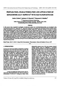
Figure 1. Schematic and MEB cross-sections of the damascene MIM capacitor stack integrated between M5 and M6 levels.
2.1 Test Structure Description All MIM capacitors are integrated between M5 and M6 levels. As M6 is a thick level ensuring the lowest resistance, access lines are dissymmetric in spite of an identical width of 10 µm (Figure 3). These dissymmetrical Metal5 and Metal6 access lines are connected to RF pads.
Dedicated MIM capacitor test structures were fabricated on 200 mm silicon substrates with a resistivity of 5.5 S/m. After completion of M5 level, the MIM cavity is etched in the V5 inter-level dielectric (SiO2) down to a M5 copper interconnect, which is used as a bottom electrode. Next, a 32 nm thick Si3N4 film is deposited by PECVD (Plasma Enhanced Chemical Vapor Deposition) in the cavity, before metallization with deposition of a TaN/Ta barrier, which acts as a top electrode, and Cu filling. Materials in excess are then removed by CMP (Chemical and Mechanical Polishing). Finally, V5 and M6 levels are completed. The resulting Cu/Si3N4/TaN/Cu stack is connected through M5 and M6 levels, as shown in Figure 1.
High-frequency behavior of such MIM capacitors is poorly known. So, DC and RF electrical characterizations are carried out to evaluate capacitor performances. A general equivalent electrical model is defined and checked over a large range of frequency (typically from 40 MHz to 25 GHz). Moreover, the impact of MIM capacitor design on its performances is investigated. Capacitor access lines are connected to RF pads in order to contact measurement probes. Capacitance is measured using a HP4274A multi-frequency LCR meter at frequencies ranging from 100 Hz to 100 KHz. Scattering parameters are extracted using an ANRITSU 37397C Vector Network Analyzer after a TRL (Thru Reflect Line) calibration de-embedding technique [2]. This technique enables to eliminate discontinuities fromcontact pads to access lines and places the reference planes at both ends of capacitors (P1-P2). Thus, only MIM capacitor characteristics are measured.
The design of such damascene capacitors has to meet copper density requirements. Thus, specific designs with comb or grid electrodes were introduced. Figure 2 illustrates the structures particularly studied. Two structures have been selected for this study. C1 and C2 are different designs of grid electrodes with the same area (3 300 µm2) leading to a capacitance of 6.6 pF. Each elementary single line of the grid is 12 µm wide.
Figure 2. Top views of studied MIM capacitors. W1 = 66 µm, L1 = 66 µm, W2 = 120 µm, L2 = 39 µm. The Simulation Standard
Figure 3: 3D view of MIM capacitor, where TM6 ~ 800 nm, TM5 ~ 300 nm, and TMIM ~ 400 nm. Page 2
November 2005
Figure 4. a) Magnetic Potential vector (A) and b) Density of Current ( ∇Σx TeΣ)
2.2 3D Electromagnetic Simulation conductivity and takes into account the skin effect. With this formulation, A and T Σ are solution of :
2.2.1 Presentation of the new simulation tool The simulations are carried out using the 3D electromagnetic field solver called QUEST QUEST. This simulator calculates the electromagnetic parameters of micro-electronic 3D geometries in frequency domain. It can extract Z, Y, S matrices and quality factors of Nports general structures.
∇x µ-1 ∇x A – ∇Σx T Σ =0 ∇Σ x(σΣ)-1 ∇Σx T Σ +j + ω∇xA=0 The magnetic potential vector A is calculated using edge finite elements [6] on a 3D regular grid (Figure 4). The electric potential vector TΣ is calculated using scalar P1 elements on a triangle meshing of the conductors surfaces (Figure 2b).
QUEST is based on a 3D field solver elaborated by SILVACO in collaboration with CEA-LETI [3][4]. It uses an original formulation of the Quasi-Static Maxwell equations where the problem is separated in two parts, an impedance and a capacitance part.
The capacitance problem comes from the equation: ∇Σ (zΣ)-1 ∇ΣφΣ =jωpΣ
The impedance problem is written using a (A, T Σ) formulation [5], where A is the magnetic potential vector, T Σ is an equivalent vector electric potential defined on the conductors surface, µ is the permeability and σΣ is a surfacic conductivity that approximates the volumic
where φΣ, pΣ are the surface potential and the surface electric charge. zΣ is a local impedance given by the impedance problem. The capacitance problem is solved using a fast and accurate computation method so called « fictitious domain method » [3].
Figure 5. Module and phase of reflexion parameters resulting from both measurement and QUEST simulator for C1 structure.
Figure 6. Module and phase of transmission parameters resulting from both measurement and QUEST simulator for C1 structure.
November 2005
Page 3
The Simulation Standard
Figure 7. Module and phase of reflexion parameters resulting from both measurement and QUEST simulator for C2 structure.
Figure 8. Module and phase of transmission parameters resulting from both measurement and QUEST simulator for C2 structure.
2.2.2 Validation of the numerical results To validate the electromagnetic simulations, a comparison with measurements is presented. Two structures C1 and C2 were simulated with QUEST QUEST. Associated 3D dimensional structures were created from GDS and technology files using the QUEST Graphical User Interface. The simulations were performed on a Sun fire V440 station with 4 ultra Sparc III1 CPUs and the corresponding CPU times calculations with 80 frequency points from 100 MHz to 25 GHz are about three hours. Results are presented in Figures 5 to 8.
MIM capacitors are considered as localized elements (i.e. no propagation effect occurs among electrodes) characterized by the serial complex impedance ZS. Scattering parameters and Z0 impedance of measurement references planes (P1 and P2) are used to calculate the B element of the transfer matrix ABCD. Then, ZS MIM capacitor impedance is directly extracted as following equation shows:
Zs = Z0
An excellent similitude between measurement and QUEST results is observed for C1 and C2 structures. Module and phase evolution resulting from measurement and QUEST simulation have nearly the same behavior. Thus, QUEST is an efficient and accurate tool to evaluate the high frequency behavior of MIM capacitors.
As a next step, MIM capacitors impedance ZS is extracted from both measurements and QUEST QUEST.
2.3.1 Modeling For a better understanding of MIM capacitor behavior in a high-frequency regime, an equivalent circuit model is established as shown in Figure 9 and discussed. The elements C and Rp figure the basic model for the capacitor, whereas additional series Rs and Ls represent the parasitic resistance and inductance due to the specific electrode design [7]-[11]. Notice that the shunt Rp is originated from dielectric losses that brings on power dissipation.
To improve the study, impact of design on MIM capacitors electrical performances is then evaluated.
2.3 Impact of Design on Capacitors Performances To investigate the MIM capacitor characteristics at RF regimes, scattering parameters and characteristic impedance of access lines have first to be extracted. M5 level access lines are thinner than M6 ones, leading to different propagation constant on the two access ports. A dissymmetrical calibration de-embedding technique is performed. However, the characteristic impedance of each level access line is calculated and their values are identical. Then, for the following extraction, M5 and M6 access lines are considered to have the same complex characteristic impedance Z0. The complex impedance of MIM capacitor is also extracted. As the longest MIM capacitor is 66 µm (in the direction of propagation), and the maximum frequency measurement is 25 GHz, corresponding to a wavelength of 4.5 mm, The Simulation Standard
(1+S11)(1+S 22) – S12 S 21 2S 21
Figure 9. Equivalent electrical model of MIM capacitors extracted at a high-frequency regime. Measurement plane references are at the capacitor borders.
Page 4
November 2005
Thus, impedance of this model was calculated and its real and imaginary parts were clearly identified. Coupled with the ZS MIM capacitor impedance, each element of the equivalent circuit model is extracted using the entire frequency range.
called QUEST is established. With this simulator, impact of new high-k dielectrics and new designs on MIM capacitor electrical performances can be predicted for future generations of RF integrated circuits based on these results. New materials, like Ta2O5, will increase the capacitance value and new design will be required to reduce the parasitic serial inductance in order to enable high-performance MIM capacitor integration for high frequency applications.
This method is used to determine each of the four parameters, C, Rp, Rs and Ls, that appears in the equivalent circuit model and their values can be seen in Table 1. The capacitance values of the two structures were verified by performing measurement with a LCR meter, resulting in a 6.65 pF capacitance for C1 and C2. Both accuracy and repeatability of this extraction were demonstrated thanks to a gap capacitance value less than 3 % between same area structures. It was also proved that static results and extracted high-frequency results are similar.
References: [1]
A. Farcy, J. Torres, V. Arnal, M. Fayolle, H. Feldis, F. Jourdan, M. Assous, J.L. Di Maria, V. Vidal, “A new Damascene Architecture for High-Performances Metal-Insulator-Metal capacitors Integration”, Materials for Advanced Metallization conference, pp 368-372, La Londe Les Maures, 2003.
[2] B. Fléchet, K, Kouicem, A, Benhayoun, G, Angénieux, “Développements relatifs aux procedures d’auto calibrage TRL ; correction d’erreurs systématiques résiduelles et calibrage dissymétrique”, 9eme Journées Nationales Microondes, JNM 1995, 4-6 avril 1995, Paris, France.
Design of MIM capacitors doesn’t act upon resistive elements Rs and Rp. However, for the same area structures, so with an identical capacitance value, when the capacitor length (L) is divided by a factor two, the inductive element Ls is divided by the same factor.
[3] S. Putot, F. Charlet, P. Witomski, “A fast and accurate computation of interconnect capacitances” International Electron Devices Meeting, pp 893-897, Washington, 1999.
This result shows the relationship between length capacitor and parasitic inductance (Ls). Extraction results confirm that the best MIM capacitor grid design is C2 for an area of 3300 µm2. So, as a design recommendation, the length of electrodes has to be minimized.
[4] F. Charlet, J.F. Carpentier, “Extraction of 3D interconnect impedances using edge elements without gauge condition” Simulation of Semiconductor Processes and Devices conference, 2002. [5] D. Albertz, G. Henneberger, “On the use of the new edge based A-A,eT formulation for the calculation of time harmonic stationary and transient eddy current field problems” . IEEE Transactions on Magnetics. Vol 36, no 4, july 2000, pp 818-822.
Extracted elements from measurements are very closed to extracted ones from QUEST QUEST. Error percentage is less than 3% on C element and 10% on Ls element.
[6] J.C. Nedelec. “Mixed finite elements in R3”, Numerische mathematic.(1980), 35, pp315-341. [7] S. B. Chen, C. H. Lai, Albert Chin, J. C. Hsieh and J. Liu, “RF MIM capacitors using High-K Al2O3 and AlTiOx dielectrics” IEEE Microwave Symposium Digest, Vol. 1, pp. 201-204, 2002.
This method represents a very good solution to evaluate the electrical performances of MIM capacitors. Coupled with the new 3D electromagnetic simulator, efficient and competitive design having best high frequency behavior, could be integrated among new generation of damascene MIM capacitors.
[8] X. F. Yu, Chunxiang Zhu, H Hu, Albert Chin, MF Li, BJ Cho, D.-L. Kwong, MB Yu, and PD Foo, “A high density MIM capacitors (13fF/ um2) using ALD HfO2 dielectrics” IEEE Electron Device Letters, Vol. 24, No. 2, pp. 63-65, 2003. [9] Chen, S.B.; Lai, C.H.; Chan, K.T.; Chin, A.; Hsieh, J.C.; Liu, J. “Frequency-dependent capacitance reduction in high-k AlTiOx and Al2O3 gate dielectrics from IF to RF frequency range “ IEEE Electron Device Letters, Vol. 23, Issue 4, pp. 203-205, 2002.
3. Conclusions From previous results, high-frequency behavior of damascene MIM capacitors integrating copper electrodes is simulated to investigate electrical performances as a function of design and material parameters. Accuracy and efficiency of a new 3D electromagnetic simulator
[10] Jae-Hak Lee; Dae-Hyun Kim; Yong-Soon Park; Myoung-Kyu Sohn; Kwang-Seok Seo, “DC and RF characteristics of advanced MIM capacitors for MMIC’s using ultra-thin remote PECVD Si3N4 dielectric layers” IEEE Microwave and Guided Wave Letters, Vol. 9, Issue 9, pp. 345-347, 1999. [11] M.Y. Yang, C.H. Huang, A. Chin, C. Zhu, M.F. Li, and D.-L. Kwong, “High density MIM capacitors using AlTaOx dielectrics,” IEEE Electron Device Letters, Vol. 24, No. 5, pp. 306-308, 2003.
Element values Structures Measurement QUEST
Rs
Rp
C
Ls
(Ω)
(KΩ)
(pF)
(pH)
C1
0.20
0.36
6.59
45.5
C2
0.15
0.39
6.75
22.0
C1
0.25
0.60
6.79
42.2
C2
0.19
0.65
6.92
19.9
© 2005 IEEE. Reprinted, with permission, from ESSDERC-05 article entitled ““Simulation and Characterization of High-frequency Performance of Advanced MIM Capacitors” by Jerome Piquet et al.
Table 1. Element values of equivalent circuit model.
November 2005
Page 5
The Simulation Standard
Numerical Analysis of GaInP Solar Cells: Toward Advanced Photovoltaic Devices Modeling M. Baudrit, C. Algora, I. Rey-Stolle, I. García and B. Galiana Instituto de Energía Solar / Universidad Politécnica de Madrid E.T.S.I Telecomunicación - Av. Complutense 38 E-28040 Madrid SPAIN Phone: (+34) 91.336.73.66 (ext. 4322); Fax: (+34) 915446341; E-mail:
[email protected]
Abstract Simulation capacities of GaInP solar cells were studied with a special emphasis on material and structural parameters. The comparison between experimental and numerical results allowed to validate the models used for such a device and permitted to extrapolate the layers structure. With this method we proved the role of the substrate in the simulation and thus its importance in the optimization process. This study is an important previous step to validate the numerical approach for multi-junction solar cell simulation in 3D.
I. Introduction In the last decade, a great activity is being carried out worldwide to achieve commercial PV based on concentrator III-V solar cells modules for terrestrial applications. Despite current concentrator products are based on silicon cells, III-V multi-junction solar cells have a tremendous potential for increasing efficiency and also to operate at higher concentration levels than silicon. Both aspects, high efficiency and high concentration, are determinant in order to achieve low cost [7]. Multi-junction solar cells including GaInP, (In) GaAs and Ge are known as super-high efficiency and are now in the main stream for terrestrial use under concentration. The high cost of these materials require concentration about 1000 suns to reduce the energy cost and a two or three junctions design for a better use of the solar spectra [1]. Efficiencies about 30% at 1000 suns [8] and 39% at 236 suns [5] have been reached and efficiencies about greater than 40% are hoped for the next years. This activity, which is in the search of a real breakthrough, is requiring very accurate models for concentrator solar cells that conduct to the highest efficiency of PV modules [2]. In order to increase the performance of such concentrator solar cells, a modeling as accurate as possible is necessary to guide the technological approaches. In this paper we will focus on the GaInP solar cell. By using a numerical analysis, we could calculate the external quantum efficiency and the performance of the device taking into account many material and structure parameters. We can analyze the behavior of the device over a wide range of wavelengths and by fitting the calculated data and the experimental ones we can extract the exact layers structure further The Simulation Standard
Figure 1. View of a Solar cell and the concentrator.
confirmed by SEM measurements. This process will be very useful to validate the simulation input parameters, to explain the behavior of a device and then to optimize the layers structure according to the requirements of this top cell into the multi-junction solar cells.
II. The Simulation Tools Traditionally, the simulated electronic devices were of micrometric scale while solar cells had always been too big t be modeled. In our case we are simulating concentrator solar ºcells, this means we reduce the cell area using an optic focusing the light on a smaller surface(see Figure 1) [6]. The typical concentration we use is about 1000 suns, which is the same as saying that the optic has an area a thousand times greater than the cell, so our active area is reduced to 1 mm2. Solar cell size is a key aspect in concentration applications that is not usually taken into account. In fact, there are not in literature specific values for the solar cell size following optimization criteria. Therefore, we determined the optimum size for a GaAs solar cell operating at 1000 suns [7]. It is about 1 mm2 and it appears as a trade-off between the influence of series resistance and perimeter recombination. More-
Page 6
November 2005
To calculate a solar cell structure, ATLAS solves Poisson’s equation, carrier continuity equation, the drift-diffusion transport model and the energy balance transport model. The previous step in order to provide accurate simulation is the insertion of specific parameters in the material related models. Indeed, depending on the growth conditions, material properties can reach a wide range of values. So we characterized intensively our materials to supply an accurate input to the simulation tool. The indispensable material related models we introduced are doping dependent mobility, doping dependent bandgap narrowing, doping and temperature dependent recombination rates. It is also important to note that a solar cell has to work over a wide range of wavelengths, and for each wavelength and doping concentration, materials have different sets of (n, k) which implies that the simulation has to allow a complete customization of the photogeneration rate, depending on the optical properties of the grown layers. The photogeneration is given by,
Figure 2. View of the photogeneration rate in the simulated structure for a wavelength of 330 nm. The photogeneration rate varies from 0 to 123 (e- h+ pairs) per (s cm3).
G=η0 Pλ αe–αy hc
over, a III-V concentrator solar cell has a very simple structure which consists of a superposition of layers; this means that we have, excepting of the metallization grid, a one dimension device. And the metallization grid has a two axis symmetry, this allow us to simulate only half of the cell in 2D (or a quarter of the cell in 3D). For this reasons it is easier to model concentrator solar cell than standard solar cell with a traditional device simulator.
with G being the photogeneration rate, P the cumulative effects of reflections, transmissions, and loss due to absorption over the ray path, y the relative distance for the given ray, h the Planck’s constant, λ the wavelength, c the speed of light and £\ the absorption coefficient calculated for each set of (n, k) value. By creating a doping, wavelength and material dependent (n,k) model, we can numerically reproduce the behavior of the solar cell all over the wavelength range of the solar spectra.
The Silvaco Software Package is a simulation software targeting the area of electronic design. This is a large suite of highly sophisticated tools that aid in the design and development of all types of semiconductor devices. The phenomena modeled start from simple electrical properties and extend to optical properties, thermal heating, interface recombination effects etc. A big variety of detailed layer growth processes and material parameters (mobilities, recombination parameters, ionization coefficients, optical parameters, etc) add accuracy to the simulation [2] and give a great versatility to the software.
IV. The Virtual Cell Ga0.51In0.49P (lattice matched to GaAs) solar cells were grown on GaAs substrates. A typical method is to simulate and optimize the cell without taking into account the substrate (so only considered as a mechanic support.). This substrate implies several changes in the infrared behavior of the device because of the smaller bandgap of GaAs. In fact, this is that we could call an “anti-BSF” effect. Consequently, if we want to correctly model the top cell we have to consider this phenomena, if not, we risk to make a erroneous adjustment and extrapolate wrong material parameters because we characterized a GaInP cell on a GaAs substrate to compare it with a simulated GaInP cell without GaAs substrate, which doesn’t count with the EQE reduction implied by the substrate in the infrared. For this we chose to virtually ‘grow’ the structure shown in Figure1 to compare the measurements with the numerical study.
III. The Solar Cell Model Silvaco ATLAS is a physically-based device simulator which predicts the electrical characteristics that are associated with specified physical design and bias conditions. By applying a set of differential equations, based on Maxwell’s laws, we can simulate the transport of carriers through a device [3]. Physically-based simulation is very different from analytical modeling which provides efficient approximation and interpolation [4] but does not provide insight, or predictive capabilities, or encapsulation of the theoretical knowledge.
November 2005
Page 7
The Simulation Standard
characteristics of the grown device. From SIM analysis we confirmed the doping profile of the layers and the SEM gave new information about the layer thicknesses. We put in evidence the numerically predicted thicknesses agreed very well with the SEM measured values, better than the theoretically grown ones (Table 1). Modeling with the substrate allowed to well determine the real structure of the device and by fitting many experimental curves we confirmed the validity of the GaAs, GaInP and AlInP parameters and equations used in the simulation software and we proved that it is necessary to model the device with the GaAs substrate in order to well analyze the structure of a device. This numerical analysis is revealed to be very powerful to extrapolate some device parameters from experimental results. In fact, once the material parameters are well defined it is possible to determine the layers thicknesses as well as to detect the eventual formation of an undesired material during the growth process. Thus the GaInP top cell is aimed to be over a GaAs tunnel diode in a triple junction solar cell device, modeling with the substrate seems to be right way to optimize such a structure taking into account the change in the band diagram due to the GaAs layer.
Figure 3 View of the substrate effect on the band diagram.
Moreover, in a double or triple junction solar cell the GaInP cell is supposed to be over a tunnel diode made of a smaller bandgap material such as GaAs or AlGaAs[5]. So, the optimization process of the top cell has to consider the presence of a smaller bandgap material layer under the PN junction and its effects on the band diagram (Figure 3).
Although we are still simulating in 2D, it is necessary to detect the pending issues in the modeling of concentrator solar cells when considering the situations appearing in their real operation. In our opinion, the most influencing ones are: different illumination spectra due to the optic, Inhomogeneous illumination distribution on the solar cell because of the focusing of the light, temperature gradients and the light impinging the cell within a cone [2]. These conditions requires a 3D simulation and, viewing the last achievements in 2D simulation of GaAs
V. Results We modeled the characteristics of the top cell using the structural and material parameters of the grown device. Then we started an iterative routine to adjust the simulated EQE to the real one, the results are shown in Figure 4. The correlation between measured and simulated results is fairly good and we clearly see the substrate lowers the EQE for wavelengths between 500 nm and 600 nm because of the electric field created by the presence of the substrate (Figure 3). The only mismatch between the two curves appears for wavelengths greater than 620 nm, further experimental data revealed the formation of an undesired quaternary alloy (InAsGaP) coupled with an optical bandgap narrowing effect explaining this difference, however we think we could model this phenomena soon. To adjust measurements and simulations we needed to modify some structural parameters such as layers thickness in the device property file. After such adjustments the results agreed but we still needed to legitimate the simulation with the substrate. So we further made some SEM, SIM and XPS measurements to know the exact
The Simulation Standard
Figure 4 Measured EQE (dots), simulated EQE with substrate (dashed line) and without substrate (solid line).
Page 8
November 2005
References
Foreseen Measured Simulation thickness thickness deduced thickness Total window/emitter/base thickness in nm
1178
1231
[1]
C. Algora, “The importance of very high concentration in third generation solar cells” Chapter 6 of book “Next generation Photovoltaic, High efficiency through full spectrum utilization”. Ed. A. Martí and A. Luque (Institute of Physics, 2004).
[2] C. Algora, M. Baudrit, I. Rey-Stolle, D. Martín, R. Peña, B. Galiana and J. R. González, “Pending issues in the modeling of concentrator solar cells”, 19th European Photovoltaic conference, Paris (2004), to be published.
1232
Table 1 Comparative of the foreseen, measured and simulation deduced thickness.
[3] ATLAS User’s Manual. Device simulation Software. Volumes I and II. Silvaco International (2002). [4] H.J. Hovel and J.M. Woodall,“Theoretical and experimental evaluations of Ga1-xAlxAs - GaAs solar cells” in Proc.10th IEEE Spec. Phot. Conf., 1973, vol.25.
and GaInP solar cells, we are ready to begin 3D modeling of GaAs, GaInP and double junction solar cells under real operation conditions.
[5] R. R. King, D. C. Law, C. M. Fetzer, R. A. Sherif, K. M. Edmonson, S. Kurtz, G. S. Kinsey, H. L. Cotal, D. D. Krut, J. H. Ermer, and N. H. Karam, “Pathways to 40%-efficient concentrator photovoltaics, 20th European Photovoltaic conference, Barcelone (2005), to be published.
VI Conclusion
[6] J. L Alvarez, M. Hernández, P. Benítez, J. C. Miñano, Nonimaging Optics: Maximum Efficiency Light Transfer VI, Proc., pp.32- 42, (2001).
The GaInP solar cells was modeled and compared with measurements. The substrate effect on the band diagram was shown to be relevant in the results of the simulation. Taking into account this effect we generate the EQE, by adjusting the layers parameters we achieved to match the experimental and simulated results. SEM measurements were done to determine layers thicknesses and it revealed that the software predicted thicknesses were closer to the real ones than the foreseen thicknesses. By fitting many curves we validate the materials and physicals models used. We put in evidence that using the substrate in the numerical process was important in order to achieve a reliable analysis of the structure. Viewing the substrate effect we also saw it has to be include in the optimization process to consider the effect will have the tunnel diode on the band diagram of the GaInP cell. We demonstrate a modeling tool can be of great interest to deduce structural parameters of a grown device once we have completely defined the materials parameters and models.
[7] C. Algora, I. Rey-Stolle, B. Galiana, J. R. González, M. Baudrit, I. García and V. Díaz, “III-V concentrator solar cells as LEDs”, 20th European Photovoltaic conference, Barcelone (2005), to be published. [8] F. Dimroth, R. Beckert, M. Meusel, U. Schubert, A. W. Bett, “Metamorphic GaInP/GaInAs tandem solar cells for space and for terrestrial concentrator applications at C > 1000 suns”, Progress in photovoltaics, vol. 9, nº3, pp 165-178, June 2001.
Acknowledgment This work has been supported by the European Commission under contract SES6-CT-2003-502620 (FULLSPECTRUM project) and by the Spanish Ministry of Science and Technology which has contributed by means of the research projects with references TIC2002-01012 and TIC2002-11391- E. We also wish to specially thank with Andrea Cappa, Alexandre Ferron and all the Silvaco Grenoble Research CEnter (G.R.E.C.E). © 2005IEEE. Reprinted, with permission, from The Proceedings of the 5th International Conference on Numerical Simulation of Optoelectronic Devices (NUSOD ‘05), ISBN 0-7803-9149-7.
November 2005
Page 9
The Simulation Standard
Calendar of Events November 1 2 3 4 Thin Flim Materials & Devices Meeting – Kyoto, Japan 5 Thin Flim Materials & Devices Meeting – Kyoto, Japan 6 7 8 9 10 SiC and Related Wide Bandgap Semiconductors – Nora, Japan 11 SiC and Related Wide Bandgap Semiconductors – Nora, Japan 12 13 14 15 16 17 18 19 20 21 22 23 24 Thanksgiving Day 25 26 27 28 29 30
December 1 2 3 4 5 IEDM 6 IEDM 7 IEDM 8 9 10 11 12 13 14 15 16 17 18 19 20 21 22 23 24 25 26 27 28 29 30 31
Bulletin Board TMA Compatibility
Silvaco announced the availability of full TMA compatibility in its 5.10.0.R release of Stanford-based ATHENA Process and ATLAS Device Simulators. Technology Computer Aided Design (TCAD) was originally pioneered at Stanford University under grants from the Defense Advanced Research Projects Agency (DARPA) during late 1970s and 1980s. It was licensed to and commercialized exclusively by Technology Modeling Associates (TMA) and Silvaco. TMA was later acquired by Avant! Corporation which was then acquired by Synopsys. In October 2004, Synopsys also acquired Integrated Systems Engineering (ISE), a TCAD provider based in Switzerland. Synopsys announced its future TCAD products would be based on the ISE software.
Silvaco TCAD Future
Silvaco will continue to provide advanced TCAD technologies based on the latest physical models for process and device simulation. Silvaco is the only company dedicated to exclusively support the Stanford TCAD legacy. Switching to Silvaco TCAD means that TMA customers do not have to recalibrate their model coefficients, re-establish their process and device simulation flows developed over many years, and learn new software.
If you would like more information or to register for one of our our workshops, please check our web site at http://www.silvaco.com The Simulation Standard, circulation 18,000 Vol. 15, No. 11, November 2005 is copyrighted by Silvaco International. If you, or someone you know wants a subscription to this free publication, please call (408) 567-1000 (USA), (44) (1483) 401-800 (UK), (81)(45) 820-3000 (Japan), or your nearest Silvaco distributor. The following trademarks and service marks are the property of Silvaco International. Registered Marks:® Virtual Wafer Fab, Silvaco. Trademarks: ™ Simulation Standard, ATHENA, Analog Alliance, Legacy, Manufacturing Tools, Automation Tools, SFLM, VICTORY, Ranger3D Nomad, VYPER, SmartSpice, PSTATS, UTMOST IV, Measure, DISCOVERY, MERCURY, Optolith,TCAD Driven CAD, TonyPlot3D, RESILIENCE, Flash, ATHENA Interpreter, Interactive Tools, DeckBuild, DevEdit, ANALOG EXPRESS, CELEBRITY, SSuprem3, ATLAS, ATLAS Interpreter, Luminous2D/3D, MC Implant, S-Pisces, TonyPlot, FastLargeSignal, SmartStats, Ferro, DevEdit3D, Interpreter, Quantum2D/3D, SDDL, Circuit Optimizer, MaskViews, TFT2D/3D, Radiant, SSuprem4, Elite, FastBlaze, Mocasim, Silicides, MC Depo/Etch, FastNoise, Clarity, Blaze/Blaze3D, Device3D, Frontier, TwinSim, MixedMode2D/3D, VCSELS, Maverick, Envoy, Giga2D/3D, FastGiga, Guardian, Scout, FastMixedMode, Laser, Dragon, Expert, Spirit, Beacon, Savage, Harm, Zenith, Vision, Scholar, SN, UTMOST, UTMOST II, UTMOST III, UTMOST IV, PROMOST, SPAYN, ExpertViews, UTMOST IV Fit, FastSpice, Twister, Blast, MixSim, SmartLib, TestChip, Promost-Rel, RelStats, RelLib, Ranger, LISA, QUEST, EXACT, CLEVER, STELLAR, HIPEX-RCR, HIPEX-Net, HIPEX-RC, Connecting TCAD to Tapeout, and UTMOST IV Spice Modeling. All other product or company names are trademarks of their respective owners.
The Simulation Standard
Page 10
November 2005
Hints, Tips and Solutions Derek Kimpton, Applications Support Manager Q. How can I create a non planar structure using III-V materials for Device Analysis when the materials I want to use are not in the ATHENA data base. A. There are many materials in the ATLAS device simulator data base that are not in the ATHENA database, primarily because most of these exotic materials are usually deposited epitaxially and very little actual processing takes place in terms of implantation, diffusion and heat treatments. However, it is often desired to create a device with non vertical side-walls or a device where a non planar realistic deposit of an inter-layer di-electric plays a key role in the device operation. In these circumstances it is necessary to use the ATHENA process simulator. However, if the process simulator does not contain the exotic materials of interest in it’s process data base, a user defined material must be used.
Figure 1. GaN/AlGaN non planar diode structre created in ATHENA with user defined materials which then get converted into known ATLAS materials.
go athena
There is a special feature in the Silvaco process simulator, ATHENA , which converts unknown user defined materials into known device simulator materials so long as the user defined material is given the exact same name as the known device simulator material.
line line line line
x x y y
loc=-1 spac=0.2 loc=1 spac=0.2 loc=0 spac=0.001 loc=2 spac=1
All that is required now to complete device construction in the process simulator, ATHENA , is to define the dopant materials as either donor or acceptor using the impurity statement.
impurity i.silicon material=GaN donor impurity i.silicon material=AlGaN donor impurity i.beryllium material=GaN acceptor impurity i.beryllium material=AlGaN acceptor
An example of the first few lines of an ATHENA deck is given below. The example demonstrates how to define the user defined material as both the starting substrate material and as a deposited layer
init material=GaN c.silicon=1e18 deposit material=AlGaN thick=1 c.silicon=1e18 divisions=8 dy=0.001 ydy=1
The impurity statements define the polarity type of each dopant for each user defined material in the structure. The user defined materials are named using the material= parameter. In this example, two materials are used that are unknown to ATHENA , namely GaN and AlGaN. However, since these materials are known to ATLAS, when the created structure is passed to ATLAS for device simulation, ATHENA will automatically convert the user defined materials into known ATLAS materials. Once again, care must be taken to ensure the user defined ATHENA material and it’s corresponding known ATLAS material are named exactly the same.
Using the material= syntax throughout the input file, a complete non planar device can be created using any material known to the device simulator, ATLAS .
November 2005
Call for Questions If you have hints, tips, solutions or questions to contribute, please contact our Applications and Support Department Phone: (408) 567-1000 Fax: (408) 496-6080 e-mail:
[email protected]
Hints, Tips and Solutions Archive Check our our Web Page to see more details of this example plus an archive of previous Hints, Tips, and Solutions
www.silvaco.com
Page 11
The Simulation Standard
Contacts: Silvaco Japan
[email protected] Silvaco Korea
[email protected]
USA Headquarters:
Silvaco Taiwan
[email protected]
Silvaco International 4701 Patrick Henry Drive, Bldg. 2 Santa Clara, CA 95054 USA
Silvaco Singapore
[email protected] Silvaco UK
[email protected]
Phone: 408-567-1000 Fax: 408-496-6080
Silvaco France
[email protected]
[email protected] www.silvaco.com
Silvaco Germany
[email protected]
Products Licensed through Silvaco or e*ECAD The Simulation Standard
Page 12
November 2005