the modeling and simulation of dc-dc converters controlled by an 8-bit ... buck converter controlled by a Microchip PIC16C74 8- ..... bl.s+bO a2.s2+ai.s+a0.
Simulation and Modeling of a DC-DC Converter Controlled by an %bit Microcontroller R. R. Boudreaux, R. M. Nelms, and John Y. Hung Department of Electrical Engineering Auburn University, AL 36849
-
Abstract Traditionally, analog control technologies have been employed to regulate the output voltage of dc-dc converters. The utilization of digital control techniques for this regulation function is currently under consideration. Critical issues in a digital control implementation include analog-to-digital conversion range, resolution and delay, calculation time, and numerical precision. Results from an investigation into the modeling and simulation of dc-dc converters controlled by an 8-bit microcontroller are described in this paper. Many of these critical issues have been modeled using Matlab'TM'and SimulinkmM)from The Mathworks Inc. Simulation results from this model are compared to experimental waveforms obtained from a buck converter controlled by a Microchip PIC16C74 8bit microcontroller. Experimental results agree well with the simulation model. The buck converter is represented by its state-space averaged model in the simulation. I. INTRODUCTION Output voltage regulation for dc-dc converters has traditionally been accomplished using analog control concepts. Interest is beginning to develop in the application of digital control principles to this regulation function [l-81. Digital control can provide several benefits over analog control methods such as less susceptibility to environmental or parameter variations, monitoring and self-diagnostics, and communication with a display or host computer. In addition, the complexity of a digital control system is contained mostly in software. Once working properly, software is more consistent and reliable than a complex analog system. Advanced control techniques are more easily implemented in a digital control system. Even though some advantages can be gained with a digital control implementation, several issues must be carefully examined. These include analog-to-digital conversion (ADC) time and resolution, PWM frequency and resolution, computational or calculation delay time, word length, calculation precision, and sampling frequency limitations. The hardware selected for a particular implementation determines the degree of impact that each of these issues has on converter performance. For example, a digital signal processor (DSP) performs calculations faster This work was supported by the Center for the Commercial Development of Space Power and Advanced Electronics with funds from NASA grant NAGW-1192-CCDS-AL. Aubum University, and the Center's Industrial Partners.
0-7803-3704-2/97 $1 0.0001997 IEEE
and more accurately than a typical 8-bit microcontroller but at a system cost increase. Another example is related to ADC resolution. Many 8-bit microcontrollers have on-chip ADCs which only have 8 bit resolution. An 8-bit ADC can only measure a voltage to one part in 255 of its reference voltage. For a typical reference voltage of 5 volts, the voltage converted to a digital representation is quantized into steps of 19.61 mV. Discussed in this paper are the results of an investigation into modeling and simulating dc-dc converters controlled by an 8-bit microcontroller using Matlab'TM'and SimulinknM),a commercial simulation package from The Mathworks, Inc. Simulation permits evaluation of the impact of these issues on dc-dc converter performance and provides insight into the design and control of a dc-dc converter with an 8-bit microcontroller. It also allows an evaluation of different converter models such as state-space-averaging and discrete time in the design of the digital controller. The accuracy of the simulation results has been evaluated through comparison with experimental results from a laboratory prototype which consists of a buck converter controlled by a Microchip PIC16C74 8-bit microcontroller [9-lo]. This paper is organized as follows. The next section contains a description of the buck converter testbed utilized as the laboratory prototype. The SimulinkMatlab model for the prototype is then presented and discussed. After comparing the simulated and actual converter waveforms, the effects of several issues related to the digital control implementation are investigated and discussed using the model. 11. BUCK CONVERTER TESTBED The buck converter in the testbed operated with an input voltage of 20V and supplied an output voltage of 12V. Two different values of load resistance were utilized in all evaluations, lOsL and la. The converter inductance and capacitance were l50p.H and lOOOpF, respectively, which yields a natural frequency of about 400 Hz. The equivalent series resistance for the inductor and capacitor are 38mQ and 30mQ respectively. The Microchip PIC16C74 microcontroller was operated at a clock frequency of 20 MHz. The switching frequency and resolution of the on-chip PWM module are software selectable from 5 MHz at 2 bits of resolution to 20 kHz at 10 bits of resolution. A 78 kHz PWM frequency (f,) at 8 bits of resolution was implemented in the testbed. The conversion time of the on-chip ADC was fixed at 16 ps. The converter
963
duty cycle was calculated using a proportional-integralderivative (PID) controller. The continuous time transfer function for a PID controller is given in equation (1).
+-+K ,
G(s)= K ,
K,s
S
where KPa is the proportional gain, Kra is the integral gain, and KDa is the derivative gain. This transfer function is converted to a difference equation for digital implementation using Euler's method [ 111 which yields
d ( k ) = K,,e(k)+ K , T C e ( j ) + K , , [ e ( k ) - e ( k - l ) ] T
(2)
1
This equation can be rewritten as d ( k ) = K P e ( k ) + K I ~ e ( j ) + K , [ e ( k ) - e ( k - l ) ] (3) j
where Kp is the digital proportional gain, KI is the digital integral gain, and KD is the digital derivative ain. The variable d(k) is the calculated duty cycle for the k sample of the output voltage and T is the sampling period. The error, e(k), is defined as the difference between the measured output voltage and the desired output voltage. In software, the error is calculated by
H
e(k) = ref - ADC(k)
(4)
where ref is a numerical reference that corresponds to the ADC result at the desired output voltage. The PID controller calculations take between 18 ps and 28 ps depending on program branches and gain selection. This PID implementation also included software to allow onthe-fly externally selectable controller gains. The code necessary to perform this function would not be necessary in a final design, which would reduce the maximum calculation time to about 24 ps. Based on the maximum controller calculation time and the ADC conversion time, a sampling frequency (l/T) of 20 lcHz was selected for the digital controller. The duty cycle calculated from (3) is passed to the onchip PWM module of the PIC16C74. Since this module operates in a synchronous fashion, the duty cycle can only be updated at the beginning of a PWM switching cycle, even if the new value is available earlier. This introduces a variable delay which depends on the point in the switching cycle when the control calculations are completed. It can be as short as a single oscillator (not instruction) cycle or as long as the switching cycle, llf, ( 1 2 . 8 ~ ) . As stated earlier, the resolution of microcontroller onchip ADCs is typically 8 bits or 256 discrete levels. The ADC is usually referenced to the microcontroller power supply, so its range is limited to 0 - 5 volts. The base resolution of the ADC is 5/255 or 19.61 mV between levels.
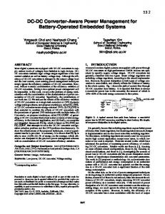
Since the buck converter in the testbed has an output voltage of 12 volts, external circuitry must be utilized to bring the voltage measured by the ADC into its range. Two problems arise if a simple voltage divider is employed. First, a loss of resolution occurs since the 256 levels are spread over a wider voltage range. If a converter output voltage of 12V corresponds to 2.5V on the ADC, the output resolution is 241255 or 94.13 mV between levels. The loss of resolution will increase steady-state errors and the magnitude of controller-induced oscillations (limit cycles). Second, a gain reduction is introduced into the system due to the voltage division. This gain reduction can be corrected in software, but resolution can only be restored in hardware. Fig. 1 describes the circuit utilized in the testbed to solve this problem. The voltage divider reduces the output voltage to a level compatible with the ADC. The op-amp UlB removes the offset and restores gain and resolution. This circuit offsets the 5V ADC range around a 12V operating point, with 12V corresponding to 2.5V on the ADC. As a result, the converter output voltage range of 9.5 - 14.5 volts is transformed to the 0 - 5 volt range for the ADC. If the converter output voltage is outside of this range, the ADC will only read its maximum or minimum value. If necessary, this "window" effect can be minimized by using multiple ADC channels on the microcontroller or a programmable gain op-amp. Using two ADC channels, one channel could measure a wide range at low resolution. Once the converter output voltage is within the 9.5 - 14.5 volt range, the second channel could be utilized to measure a small range at high resolution. Examination of Fig. 1 reveals that the circuit is inverting; however, this is easily accounted for in software by changing the sign of the calculated error. For many applications, this circuit does not require precision op-amps to obtain satisfactory performance.
964
Fig. 1. Offset Circuit. 111. THE SIMULINIUMATLABMODEL The objective of this model is to include non-ideal effects such as analog-to-digital conversion range, time and delay, calculation delay, quantization, and numerical precision. The Simulink block diagram for the buck converter testbed described in the previous section is given in Fig. 2. Note that the buck converter is represented by a statespace-averaged model; other buck converter models could
easily be substituted into this diagram. The output voltage of the converter is labeled V, in this figure. The effect of the offset circuit is simulated by the first block in the feedback path ‘Suml’, which subtracts an offset voltage of 9.5V from the output voltage. Referring to Fig. 1, a low-pass filter is added to the output of the offset circuit to remove noise and buffer the ADC input. This is modeled by the block ‘ADC RC filter’ in Fig. 2. The next block in the feedback path models the ADC conversion delay, which is 16 ps for a Microchip PIC16C74 operating with a 20 MHz oscillator. A 20 kHz sampling frequency is implemented with a zero-order hold block. The next three blocks in the feedback path convert the 0 - 5 volt signal to an 8-bit representation in the range of 0 - 255. The value out of these blocks is referred to as the “ADC result” and is compared to the binary representation of 128, which corresponds to the desired output voltage of 12V. It is also possible to simulate a programmed soft start or reference change using the ‘Software Ref Change’ block. The error signal e(k) is the input to the PID controller and is generated by the block ‘Sum2’. Note the limiters in both the proportional and integral paths of the controller which impose bounds on the intermediate numerical calculations similar to that in the actual software. Multiple bytes are actually utilized in the PID calculations in the microcontroller to avoid intermediate numerical error. However, the on-chip PWM module for the PIC16C74 only implements an 8-bit representation for the duty cycle at the selected PWM frequency (78 kHz for the PIC16C74 with a 20 MHz oscillator). For this reason, the duty cycle, which is the output of the block ‘Sum3’, must be limited to be between 0 and 255. It is rounded up to the nearest integer and then converted to a number between 0 and 1. Calculation delay is then modeled with a fixed 30 ps delay. Recall that the PID calculations require between 18 - 28 ps depending on the value of e(k) which determines the sequence in which the software commands are executed.
IV.COMPARISON TO EXPERIMENTAL RESULTS The degree with which the model of Fig. 2 predicts converter behavior was evaluated by comparing the converter response from the simulation and the testbed. Fig. 4 is a plot of the actual output voltage and the output voltage predicted by the simulation. In this plot, the output voltage of the converter is changed between 10 V and 14 V by changing the software reference. This is accomplished in Fig. 2 with the block labeled ‘Software Ref Change’ and in the testbed through the software in the microcontroller. Note that the simulation and experimental results are closely matched. As can be seen in Fig. 4, the load is la and the gains for the digital PID controller are Kp = 1/8, KI = 1/64, and KD = 2. Note in Fig. 4 that two different simulations are plotted with oscilloscope data from the testbed: one from the block diagram of Fig. 2 which is referred to as the non-ideal simulation and another from the block diagram of Fig. 3 which is referred to as the ideal simulation. Fig. 3 is a
965
simplified version of Fig. 2. The feedback path is reduced to two components: the zero-order hold which simulates the 20 kHz sampling frequency and the block which provides the proper scale factor. As a result, the ideal simulation has infinite ADC resolution and discretization effects, but does not have quantization effects. The forward path is also simplified. The limiters in the PID controller have been removed. The most significant reduction is the elimination of the calculation delay. As can be seen in Fig. 4, the two simulations are very close even with the many simplifications. Fig. 5 is another plot of the output voltage as it is changed from 1OV - 14V through a reference change. The load remained at la for this experiment. However, the PID controller gains have been changed to Kp = 1/4, KI = 1/32, and KD = 2. Note that the response of the converter is underdamped for these gains. As expected, the non-ideal simulation is closer to the experimental results obtained from the testbed than the ideal simulation. Examination of Figs. 4 and 5 alone could lead to the conclusion that the ideal simulation predicts approximately the same response as the non-ideal simulation with less model complexity. Figs. 6 and 7 contain startup transients for the converter. In both figures, the simulations predict a faster response than measured with the testbed. The non-ideal simulation response has a similar shape to the experimental response. The impact of removing the calculation delay and the offset circuit can be seen in the startup transients from the ideal simulation. When the output voltage is outside of the 9.5V - 14.5V range, the ADC saturates at its minimum or maximum value in the non-ideal simulation. For the ideal simulation, the actual voltage is converted by the ADC over the full range of output voltages. As a result, the effects of the offset circuit are more pronounced in the startup transient when the output voltage is out of range. This was also verified by the responses of Figs. 4 and 5 where the output voltage remains in range. Another important result can be seen by comparing Figs. 4 - 7. Note that a better reference change response is obtained with the gains of Figs. 4 and 6. However, a faster startup transient is obtained with the gains of Figs. 5 and 7. This illustrates the potential advantage of using different gains depending on the operating condition of the converter. For example, one set of gains could be utilized during startup and another set for small perturbations around steady state. The ability to change gains based on converter operating condition would be very difficult with an analog controller; however, a digital controller could perform this function quite easily. V. CONCLUSION The topic of this paper has been the simulation and modeling of dc-dc converters controlled by an %bit microcontroller. A buck converter testbed was modeled and simulated using SimulinkMatlab. Numerous simulations have been performed with this model, and the results are
summarized as follows: 1) The offset circuit increases ADC resolution resulting in smaller steady-state error. If the output voltage is measured directly, it must first be scaled to a level between 0 and 5 volts. Assuming that the desired output voltage of 12V corresponds to 2.5V at the ADC pin, a loss of resolution occurs because the output voltage is effectively represented by 255 levels separated by 94.1 1 mV. This loss of resolution can produce oscillation if the actual output voltage is between two of the 255 levels. The offset circuit takes the range from 9.5V - 14.5V and translates it to the 0 - 5V level of the ADC to minimize the loss of resolution and reduce the magnitude of an oscillation induced by discretization in the digital controller. Controller-induced oscillations typically limit cycle around 1 or 2 levels. Reducing the resolution (by omitting the offset circuit) will increase the magnitude of these limit cycles. The offset circuit does introduce a nonlinearity into the system whenever the output voltage falls outside of the 9.5 - 14.5 V range. The response of the converter is not affected by the offset circuit if the output voltage falls within this range. In fact, simulation results from the non-ideal and the ideal simulation are nearly identical if the output voltage is in this range. This also indicates that the effect of the delays and quantization is very small. 2) Simulation results appear to be sensitive to the values used for the equivalent series resistance of the output capacitor and inductor in the buck converter. Neglecting these values reduces the damping in the model which increases overshoot and oscillations. 3) The simulation results are not as sensitive to the ADC conversion and calculation delays as they are to the offset circuit and equivalent series resistances. This results from the 20 kHz sampling frequency being much greater than the bandwidth of the system (400 Hz). 4) Quantization affects steady-state error, limit cycles, and controller-induced oscillations. 5) Simulation results comparable to the experimental results were achieved using only a state-space-averaged model for the buck converter. It may be possible to design digital controllers for dc-dc converters using familiar state-spaceaveraged models instead of more sophisticated models such as discrete-time models. 6) Simulation can be a useful tool in the analysis and design of dc-dc converters controlled by an 8-bit microcontroller. For small perturbations about the steady state, responses from the ideal and non-ideal simulations are almost the same. The most significant difference between the simulations occurs when the output voltage is outside of the range of the offset circuit. As a result, the non-ideal simulation should be utilized during a startup transient, a large load transient, or a large change in the input voltage, while the ideal simulation could be utilized for small perturbations. 7) Recall that the PID calculations require between 18 and 28 p to determine the new value of the duty cycle. Considering the synchronous operation of the PWM module, the delay in updating the duty cycle may be between 0 and 12.8 ps.
Therefore, a variable delay of 18 - 42.8 ps exists in the testbed between the calculation of e(k) and the update of the duty cycle. This variable delay is not modeled in the simulation and may be one reason for the difference between the non-ideal simulation and the experimental results. REFERENCES [l] R. Vinsant, J. DiFiore, and R. Clarke, “Digitallycontrolled SMPS Extends Power System Capability,” Power Conversion and Intelligent Motion, Vol. 20, No. 6, June 1994, pp. 30-37.
[2] J. DiFiore, R. Vinsant, and R. Clarke, ”Digital Control Converts Power Supply into Intelligent Power System Peripheral,” Ninth International High Frequency Power Conversion Conference, April 1994, pp. 2-6. [3] S. Canter and R. Lenk, “A Low Cost Microprocessor Based Satellite Power Control Unit,” Ninth International High Frequency Power Conversion Conference, April 1994, pp. 7-17. [4] J. Paulakonis and J. Dunn, ”Power Factor Corrected Microcontrolled UPS, Ninth International High Frequency Power Conversion Conference, April 1994, pp. 18-26. ”
[5] C. P. Henze and N. Mohan, “A Digitally Controlled AC to DC Power Conditioner That Draws Sinusoidal Input Current,” IEEE Power Electronics Specialists Conference, June 1986, pp. 531-540.
[6] R. R. Boudreaux, R. M. Nelms, and John Y. Hung, “Digital Control of DC-DC Converters: Microcontroller Implementation Issues,’’ Combined Proceedings of HFPC Power Conversion & Advanced Power Electronics Technology, Powersystems World’96, September, 1996, pp. 168-180. [7] R. R. Boudreaux, R. M. Nelms, John Y. Hung, and L. C. Mathison, “Digital Control of a Buck Converter Using an 8bit Microcontroller,” Tenth International High Frequency Power Conversion Conference, May 1995, pp. 238-25 1. [8] P. Kocybik and K. Bateson, “Digital Control of a ZVS Full-Bridge DC-DC Converter,” Tenth Annual IEEE Applied Power Electronics Conference Proceedings, Vol. 2, 1995, pp. 687-693. [9] Microchip DataBook, Microchip Technology, Inc., Chandler, Arizona, 1994. [ 101 Microchip Embedded Control Handbook, Update I, Microchip Technology, Inc., Chandler, Arizona, 1995.
[ 111 C. L. Phillips and H. T. Nagle, Digital Control System Analysis and Design, Prentice-Hall, New Jersey, 1995.
966
Square Wave t102d
PID CALCULATION
I
I
-
I
Clock
Zem-Order
255 max
CElL
Limlt to 8blt poslbve values
Quantlza (Integer Round Up)
Hold
Scale 0-5v IO 0-255
20 kHz sample
ADC Conversion Delay (mntlnuous) 16 us
ADC RC 'Iter
Offset
fc = 100 kHz
Fig. 2. Non-Ideal Simulation with Full Converter Model and Software Reference Change.
Square Wave
i102d
PID CALCULATION
. .. Somare Ref Change
Proportional
10'255l5 to 14'255l5
Sum2
ko
ki'isum(k)
bl.s+bO
Integral
a2.s2+ai.s+a0
iw
_.D
isum(k-1)
s-domain model
kd'[e(k)*(k-l)]
Clock
Derivative kd
Zem-Order Hold
Scale 0-5V to 0-255
20 kHz sample
Fig. 3. Ideal Simulation with Full ConverterModel and Software Reference Change.
967
-
15
14
3
4
23
..
I al
9 6 12 >
Non-Ideal Simulation (SimulinkTM)
5 2 11
10
i ..
..............................
0.005
0.01
0.015
0.025
0.02
0.03
0.035
0.04
time (seconds)
Fig. 4. Simulated and Actual Output Voltage During Software Reference Change.
15 Non-Ideal Simulation
.....................
. . . . . . . .(Sir?Uli?kTM).. . . .
14
14 Volt Setpoint (SimulinkTM)
$13 5 5 1)
$12 >
5 1C 2. Load Resistance k,=1/4 k,=1/32 k,=2
3 11
10
9
. . . . . . .10 . . .Volt . . . .Setpoint .........
0.005
.........................
I
0.01
0.015
0.02
0.025
time (seconds)
Fig. 5. Simulated and Actual Output Voltage During Software Reference Change.
968
0.03
0.035
0.01
~
14 1
I
I
I
I
I
I
1
-
.................
7
Experimental (Oscilloscope ) Non-Ideal Simulation (Simulinkm) Ideal Simulation (Simulinkm) . . . . . -+1%Band Around V,
I
1 S2 Load Resistance k,=1/8 k,=1/64 b=2
0
0
I
I
I
I
I
I
I
0.001
0.002
0.003
0.004 time Iseconds)
0.005
0.006
0.007
0.00;
Fig. 6. Simulated and Actual Output Voltage During Converter Startup.
.. .. .. .. .. .. .. .. .. .. .. .. .. .. .. .. .. .. .. .. .. .. .. .. .. .. .. .. .. .. .. .. .. .. .. .. .. .. .. ..
- Experimental (Oscilloscope )
_ _
.....
Non-Ideal Simulation (Simulinkm) Ideal Simulation (Simulinkm) *I% Band Around V,, 1 S2 Load Resistance k,,=1/4 k,=1/32 k,=2
0
0
I
I
I
I
I
I
I
0.001
0.002
0.003
0.004
0.005
0.006
0.007
time (seconds)
Fig. 7. Simulated and Actual Output Voltage During Converter Startup.
969
0.00