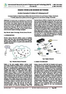
SOC design of a Low Power Wireless Sensor network node for Zigbee Systems 3
#Ninad B. Kothari1, T.S.B. Sudarshan2, S. Gurunarayanan1, Chandrasekhar 1
2
Electronics & Instrumentation Group, Computer Science Group Birla Institute of Technology, Pilani, India 333031 {ninad, tsbs, sguru}@bits-pilani.ac.in 3 CEERI, Pilani, India 333031,
[email protected]
Abstract We present a SoC architecture of a wireless sensor network node for the Zigbee protocol which can both serve as an independent chip or also be incorporated as a component of a larger system. We describe the attributes that a design must possess in order to function effectively in a densely populated sensor network and then discuss the proposed Architecture design adhering to these attributes. We draw comparisons between proposed architecture and some already existing ones and finally highlight the advantages of using the proposed SoC design. 1.
in critical and hazardous places. Also it is neither affordable nor feasible to have batteries changed every few days. Technologies like 802.11.x and Bluetooth cannot serve this segment as they have extremely high power consumption due to the high throughput they deliver. Comparison of various wireless technologies is as shown in Fig 1 [1]. Hence standards like Zigbee and Z-wave have emerged recently for this market sector.
INTRODUCTION
The wireless revolution with smart sensor dust, computing power spread everywhere like oxygen, industrial control systems, home security etc. all being managed by intelligent self forming and self correcting wireless sensor networks is a dream fast becoming a reality. In recent years there has been an exponential growth in wireless technology and ever increasing need for throughput. This demand is mainly due to requirements like huge amount of data transfer, internet, video conferencing, and media on demand etc. The need for higher performance for this niche market is currently being served by existing and wellestablished technologies like 802.11.x and Bluetooth. However, there are certain segments, which do not require such heavy data transfer capacities. For example an industrial control system would generally be required to monitor and control pressure sensors, temperature sensors, valves, switches, pumps, control unit etc in synchronization with the entire industrial process. In such systems wireless sensors would be deployed in critical areas, which would collect data at specific time intervals, send the data to a central wireless node which based on certain pre-fed information would make decisions to turn on or off a switch, pump, control unit etc.. Such information transfer hardly sums up to a few bytes and hence low data rates would suffice for such implementations. The main and stringent requirem1ent for such systems is power consumption, as seldom, power sources are available
Fig. 1: A comparison between different wireless technologies [6].
Zigbee is a new personal area network radio communications standard, which has been designed to serve low data rate, low power segments. The Zigbee stack is as shown in Fig 2. IEEE 802.15.4 [1] defines the PHY and MAC layers where as the consortium of companies called the Zigbee Alliance [2] define the upper layers.
Fig. 2: The Zigbee Stack [2].
Table 1 [2] gives the protocol specifications. Zigbee devices can be classified according to their physical features as Fully
1-4244-0716-8/06/$20.00 ©2006 IEEE.
462
Functional Devices (FFD) and Reduced Functional Devices (RFD) [1], [2]. Here we propose a generic architecture that can be used as either an RFD or an FFD. TABLE 1: ZIGBEE PROTOCOL FEATURES
Property Raw data rate
Range 2 – 250 kbps
Battery life Range
Battery life must be as long as the shelf life 10 cm to 10m or up to 100 m with tradeoffs
Latency
10-50 ms or larger than 1s
Location awareness Nodes network Topology
Optional
Freq band
per Up to 65534 (approx) Star and mesh or cluster Unlicensed and international band
The chip based solution for a Zigbee sensor network node, by the conventional method would be to consider any conventional microcontroller, modify its system architecture so as to reduce the power consumption, add few sleep states and then have a software implementation of the network stack. There are quite a few implementations, which follow this methodology like Microchip [15], Atmel [18], etc. This method, though very fast to implement would not give an optimal solution for Zigbee. Here we propose a SoC design for Zigbee sensor node architecture. 2.
ARCHITECTURE
The primary goal being to reduce the power consumption, various tasks of the protocol were identified, which has to be performed without exception at every new packet arrival. If a dedicated hardware is implemented which can perform these tasks without waking up the Main Processor Core, a large amount of energy will be saved. There are other tasks like AES encryption; decryption and CRC generation, which if performed in software by the Main Processor would consume large amount of energy. Hence it would be beneficial if hardware were dedicated for such tasks also. In the above process the complete MAC functionality and part of the NWK layer functionality is designed into dedicated units of hardware thus saving power, which would otherwise be consumed in executing software routines on the Processor. The main block diagram of the architecture is as shown in Fig 3. and the data flow diagram of the system is shown in Fig. 4. Due to lack of an available Zigbee compliant RF block for on chip integration, a off-the-shelf RF Zigbee compliant chip by Chipcon is used [16]. 3.
IMPLEMENTATION
The complete SoC has been designed using custom and tailor made blocks designed for optimal power savings. The division of labour for the protocol has been carried out in such a way so as to allow the power management unit (Queue
463
Fig 3: Main Block diagram of SoC
controller) to have maximum freedom of transferring nonfunctional units into sleep mode. A. Bus Architecture On a single chip when many different units have to communicate with each other on a regular basis, generally shared bus architectures like the AMBA or IBM CoreConnect would be preferred [8] [9] [10]. This will be apt for a design where two or more bus masters are competing with each other to control the bus. But in the proposed architecture, the data is transferred primarily in sequence or in steps, and seldom does such a situation arise. Hence, for such a system, shared bus architecture consumes more power due to the entire bus capacitance being charged and discharged during data transfer. Here we propose, to use a multiplexeddemultiplexed architecture as shown in Fig 5. B. Queue Controller The name Queue controller is a misnomer as it actually undermines the real work done by this module. The main functions can be listed as: x Providing a 4-wire SPI interface for the Chipcon CC2420 IC and configuring the CC2420 at startup using the command strobes and configuration registers. x Acting as Serial-In Parallel Out module as well as a Parallel-In-Serial-Out module for communication with CC2420. x Maintaining Data Structures to keep track of data packets and free space in the I/P and O/P buffers. x Transfers data from the I/P buffer to the MAC, CRC Check Unit and AES Decryption units. x It is the Power Management Unit of the SoC. x It also provides the interface for the Main Risc Core to communicate with CC2420.
Fig. 5: Multiplexed-Demultiplexed Bus scheme
Fig. 6: Simplified block diagram of MAC unit
The major design issues are: 1) If the MAC unit has to check whether the incoming packet is from a connected node or not, then it needs access to the Addresses in the routing table. The routing table would be in the Main Memory for accessing memory Main RISC Core has to be woken up. But this defeats the very purpose of having a separate MAC unit. Hence a small routing table has to be maintained inside the MAC unit. 2) For each new node that gets added, the MAC Unit table also has to be updated. Hence a processor interface is provided. 3) To search for a 64-bit or 16-bit address out of 128 lines is a very power intensive operation if not done properly. Hence to save both power and time we have implemented a hardware hash search engine. 4) One of the critical decisions that has to be made is the associability each node can have (IE: how many nodes (FFD’s or RFD’s) can be associated with another FFD [2]. We have assumed that maximum 128 nodes can be linked with any other node at a time. Fig 4: Data flow diagram of the system
For further power saving the Queue Controller has been divided into four sections Queue1, Queue 2, Queue 3 and Queue 4 based on the functionality. C. MAC Unit This is one of the most critical units of the system as this along with the CRC Unit decides whether the Main RISC Core will have to be interrupted from the Sleep mode as shown in Fig 6
464
D. CRC Check and Generation Unit Wireless communication is known to be one of the most prone to channel and transmission errors. The IEEE 802.15.4 standard defines a 16-bit (Cyclic Redundancy Check) CRC [19] check in order to maintain the message validity. This check is performed on the PHY payload [1] and finally the 16-bit CRC result is post fixed at the tail of the packet. Hence if the CRC check gives a negative result, then the Main RISC Core is not interrupted and the packet is discarded. Fig 7 gives a simplified diagram of the checking hardware.
E. AES Encryption and Decryption Unit The AES Decryption Unit is woken up only after the packet passes the MAC and CRC Units. The packet is completely transferred to the 128-byte memory. As the AES needs to talk to the Queue Controller (Queue 2), MAC as well as the Main RISC Core it has been provided with the necessary interfaces as shown in Fig 8 [5].
2) A normal network stack implementation would generally have quite a large percentage of Call and Branch instructions. Hence the extra register space also act as shadow registers which can save the energy and time spent in context switching. Of course this is a compiler dependent implementation. 3) A software stack implementation would generally need a lot of flag setting resetting facilities. To do this on a conventional CPU would waste critical registers. Hence we built special instructions, which would make registers behave as bit addressable. Example: STBT (set bit), CLRBT (clear bit), BRBST (Branch if Bit Set), BRBCLR (Branch if Bit Clear), BRLT (Branch on Less than), BRGT (Branch on Greater than) etc. 4) The MRC needs to communicate with the internal units like MAC Unit, Queue Controller, CC2420, AES Unit for reading data or to write data to these units and to configure them. All the configuration registers are memory mapped. 4.
Fig 7: Simplified hardware of CRC Checking Unit
Fig 8. Simplified block diagram of the AES block with MAC, Queue and Processor interfaces.
F. Main RISC Core (MRC) Finally when the packet is decrypted in the AES Decryption Unit it interrupts the MRC. The MRC stores the packet in the main memory and starts the computations. Design issues for the MRC are as follows: 1) The MRC needs to be a very low power unit as well as have reasonable performance. For this reason we choose to implement it on the lines of the MIPS 5-stage pipeline [20],[21]. As a Zigbee node is not expected to have large computational resources [3], [4], [6] we removed the Floating Point Unit out of the MIPS ISA and instead included extra registers which could function similar to the scratchpad memory of a microcontroller.
465
RESULTS AND CONCLUSION
Qualitative and quantitative analyses of the power consumption in sensor network node were carried out. The Transceiver (Radio) and Microcontroller implementations were examined. Architectural modifications were designed after this analysis to maximise power savings. Consider an average AAA battery, which would normally be used for such implementations. The average battery energy capacity is around 750 mAh [13], [6]. If the battery delivers around 3 V for a complete discharge then the Energy or the Output capability [13] is approx 2700 Joules. Hence for a nonrechargeable battery this is the total amount of energy it can deliver during its complete lifetime. Now consider an average Zigbee node. When a packet is received it would go through the following steps: It is stored in a buffer, might be in the scratchpad memory of the microcontroller. A CRC check would be performed to check the validity of the packet. An address check would be performed using the routing table that would be stored in the RAM of the microcontroller. If after the CRC or the address check there is a mismatch then the packet has to be discarded. Otherwise, AES decryption would be carried out. Finally, computation on the actual payload is done. If required a reply would have to be generated based on the data already present on the FLASH of the microcontroller. In any moderately dense Zigbee network 90 percent of the packets received would have to be discarded, 6 percent would be meant for forwarding and the rest would be actual data for the node itself [6]. In any low power microcontroller an average instruction would take around 4nJ to 12nJ per instruction [11], [14], [15], [17] An average radio would take around energy equivalent to 800-1000 instructions to receive or transmit a single bit [7], [16] that is around 1800nJ to 2400nJ per bit. The average size of the Zigbee packet is 60 to 70 bytes [6]. If the packet goes through few initial steps after which it is discarded then to implement this in a conventional microcontroller requires atleast 2500 to 3000 instructions. If a
packet travels through all the steps, then it requires around 10K to 12K instructions. Test scenario Consider a densely populated network with 100 nodes, which can communicate with each other such that every node transmits data atleast once in a second. Such a situation would be easily found in any modern industry or office with a Zigbee implemented network. Hence each node would have to listen to a packet every 10 ms. If the network works at 250kbps, an average sized packet would be completely received within 2.24 ms. To process the packet till few initial steps before it is discarded, on a microcontroller with a clock frequency of 10MHz would take 0.3 ms while to process the packet through all the steps would take 1.2 ms. Thus for 1 second, CPU run time is: 90 * 0.3 ms + 10 * 1.2ms = (approx) 40ms (1) And CPU idle time is: 1 second – 40 ms = 960 ms (2) In idle mode (2) the energy dissipated for 960ms is 28.8 micro joules [14], [15], [18]. Similarly energy spent in running the 90% packets first few steps for 1 second is 1.5 mJ while the rest of the packets through all the steps is 1 mJ. The energy spent during the receiving and transmitting of packets for 1 second for the above scenario is around 1.1 mJ. Thus total energy spent is around 3.5 mJ. Under the above conditions a standard AAA battery would last approximately for around 250 hours. For the above power calculations the power dissipated by the remaining modules of the microcontroller like ADC, DAC, Watchdog timers, etc [15],[18] has not been taken into account. This shows the importance of reducing the CPU wake up time. Results The complete architecture has been designed with each block coded and verified. Blocks like the CRC Unit, AES Unit and the MAC units have been synthesized and preliminary power figures have been obtained which is shown in Table2. It must be noted that the above figures have been obtained without using any low power circuit techniques and hence they afford us much more space for further reduction of the power figures. TABLE 2: POWER AND GATE COUNT OF IMPLEMENTED UNITS. THE POWER FIGURES ARE OBTAINED USING MAGAMA TOOLS ON 0.13 MICRON TECHNOLOGY
Module Name AES Unit MAC Unit
Power Dissipation (mW) 0.074 0.019 (dependant on worst case scenario)
Gate Count (K) 12.78
CRC Unit
0.012
1.2
1.7
REFERENCES [1] IEEE Std 802.15.4, “Wireless Medium Access Control (MAC) and Physical Layer (PHY) Specifications for Low-Rate Wireless Personal Area Networks (LR-WPANs)”. [2] Homepage of ZigBee™ Alliance, http://www.zigbee.org/ [3] Zeroing in on ZigBee (Part 1) :Introduction to the Standard by Pete Cross. Feature article in Circuit
466
[4]
[5]
[6]
[7]
Cellular. www.circuitcellar.com/library/print/0205/Cross175/ Cross-175.pdf Zeroing in on ZigBee (Part 2) :Introduction to the Standard by Pete Cross. Feature article in Circuit Cellular. www.circuitcellar.com/library/print/0305/Cross176/2 503014-Cross%20Part%202.pdf Ninad B. Kothari, T.S.B. Sudarshan, Shipra Bhal, Tejesh E. C.. S. Gurunarayanan, “Design of an efficient Low power AES engine for Zigbee systems”, Progress in VLSI Design & Test, ISBN 81-88901-245, Elite Publishing House Pvt. Ltd., Goa, August 2006, pp 264-272. Jose A. Gutierrez et al, “802.15.4: A Developing Standard for Low-Power Low-Cost Wireless Personal Area Networks”, IEEE Networks, Vol.15 no. 5, September-October 2001, pp 12-19 Chris Karlof et al, “TinySec: A link layer security architecture for wireless sensor networks”, 2nd international conference on Embedded networked sensor systems, Baltimore USA, 2004, pp 162-175.
[8] Tsai, C. A. et al, “ARM-Based SoC Prototyping Platform Using Aptix”, iCEER – 2005 Conference, Tainan, Taiwan, March 2005.
[9] AMBA Bus Architecture Datasheet [10] ] IBM CoreConnect Datasheet [11] V. Raghunathan et al, “Energy aware wireless microsensor networks”, IEEE Signal Processing Magazine, vol. 19, no. 2, March 2002, pp. 40-50. [12] Rajeshwari Banakar et all, “Scratchpad Memory: A Design Alternative for Cache On-chip memory in Embedded Systems”, Proceedings of the tenth international symposium on Hardware/software codesign, 2002, Pages: 73 – 78. [13] ] http://www.greenbatteries.com/batteryterms.html [14] Gaurav Mathur et al, “Ultra-Low Power Data
Storage for Sensor Networks”, Proceedings of IEEE/ACM Conference on Information Processing in Sensor Networks (IPSN-SPOTS), Nashville, TN, April 2006.. [15] Microchip PIC18F4620 nanoWatt technology microcontroller datasheet [16] Chipcon CC2420 Zigbee compliant radio datasheet [17] ST Microelectronics TI-MSP 430 datasheet. [18] ATMEL ATmega1280 8-bit AVR microcontroller datasheet. [19] Microchip documentation, AN730, CRC generating and checking. Available at http://www.ccs.vstu.edu.ru/sprav /Microchip/download/appnote/category/crc/00730a.p df [20] D A Patterson and J L Hennessy, Computer Organization: A Hardware Software Approach, Morgan Kauffmann, 3rd Edition, 2002. [21] J L Hennessy and D A Patterson, Computer Architecture: A Qualitative approach, 3rd Ed., Morgan Kaufmann, 2002.