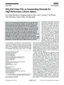
Electrochemical and Solid-State Letters, 6 共5兲 A75-A79 共2003兲
A75
0013-4651/2003/6共5兲/A75/5/$7.00 © The Electrochemical Society, Inc.
Structured Silicon Anodes for Lithium Battery Applications Mino Green,a,*,z Elizabeth Fielder,a Bruno Scrosati,b,* Mario Wachtler,b and Judith Serra Morenob a
Department of Electrical and Electronic Engineering, Imperial College, London SW7 2BT, United Kingdom Department of Chemistry, University of Rome ‘‘La Sapienza,’’ 00185 Roma, Italy
b
Pillar arrays fabricated on silicon substrates have been tested as potential anodes for lithium batteries. Electrodes of array characteristics, diameter 580 ⫾ 150 nm; fractional surface coverage 0.34; height 810 nm are reported here. Cyclic voltammetry 共CV兲 and cyclic galvanostatic tests of alloying/dealloying of electrochemically produced lithium with silicon were carried out, and results correlated with SEM studies. Aerial current densities in the low and fractional mA cm⫺2, and voltage 25 mV to 2 V 共vs. L/Li⫹) were used. CV features correspond to various Zintl phase compounds 共ZPCs兲. Structured electrodes of Si pillars maintained their structural integrity throughout cycling; planar Si electrodes showed cracks 共2 m features兲 after 50 cycles. A model is advanced in which lithium diffuses through a layer of ZPC to react with Si: growing ZPCs plastically deforms where necessary. Upon lithium dealloying vacancies coalesce to form voids at the ZPC/Si interface, Si rejoins the substrate, or precipitates out as a nanocrystalline material, and the voids appear as a fine pattern of cracks, looking like dried mud. The extra surface area that a pillar structure can confer on Si electrodes is essential and makes it practical to consider the possible eventual use of such anodes in integrated battery structures. © 2003 The Electrochemical Society. 关DOI: 10.1149/1.1563094兴 All rights reserved. Manuscript submitted October 18, 2002; revised manuscript received January 22, 2003. Available electronically March 5, 2003.
Silicon is recognized as a potentially high energy per unit volume host material for lithium in lithium battery applications.1 Attempts at realizing this potential have met with only partial success when nanocomposites of silicon powder and carbon black have been used.2 The major technical problem associated with the use of silicon/lithium appears to be the mechanical failure brought about by the repeated large volume expansion associated with alloying.1c,3 Metallic and intermetallic anodic host materials, other than layer materials such as graphite, are reported to disintegrate after a few lithium insertion/extraction cycles3,4 unless in fine powder form 共submicrometer range兲. Since we are interested in finding a way to make a lithium battery integrated onto a silicon chip we need to find a solution to this materials problem. Our proposal is to use a nanostructured silicon anode, discussed below. It is envisaged that the principle applications area for lithium batteries integrated into a chip is in the medical field. Thus the well-developed practice of cochlea implants appears to be an area that would benefit from an integrated battery supply.5 The characteristics of the silicon-lithium system, with its set of Zintl phase compounds 共ZPCs兲 is central to this work. Wen and Huggins6 reported equilibrium emf data for the liquid system at 415°C 共shown in parentheses below兲 and the solid system at room temperature7 共shown without parentheses below兲. Their results 共in millivolt vs. Li兲 are Si/Li12Si7 -582 (332); Li12Si7 /Li7 Si3 520 (288); Li7 Si3 /Li13Si4 -428 (158); Li13Si4 /Li21Si5 -⬃300 (44). It is proposed here that structured electrodes consisting of submicrometer diameter pillars of silicon fabricated on an n-type silicon wafer should be made 共see later Fig. 3兲. 共In a final version these pillar structures may be made on wafer-bonded silicon-on-insulator8 substrates.兲 The basic notion is that such submicrometer anode structures, by virtue of their small size and configuration, should be able to tolerate the massive volume changes occasioned by lithium alloying/dealloying. The volume of the first ZPC, Li12Si7 , is 2.17 times larger than that of the host silicon from which it is made 共we envisage that integrated batteries will be restricted mainly to this composition兲. Therefore, any structure must be potentially capable of accommodating this increase: such a restriction means that the silicon pillars should not exceed a fractional surface coverage 共F兲 of ⬃0.5.
* Electrochemical Society Active Member. z
E-mail:
[email protected]
Experimental Structured electrode surfaces.—The structured electrode may be made using conventional deep UV lithographic methods, but we chose to use an economical method available to us, namely, ‘‘island lithography.’’ This method employs cesium chloride as the resist in the lithographic step in the fabrication of pillar arrays. It works as follows. A thin film of CsCl is vacuum deposited on the clean, hydrophilic surface of the Si substrate. This system is then exposed to the atmosphere at a controlled relative humidity. A multilayer of water adsorbs on the surface, the CsCl is soluble in the water layer 共being more soluble at places of higher radius of curvature兲. The CsCl reorganizes into a distribution of hemispherical islands, driven by the excess surface energy associated with CsCl surface curvature. Such arrays are useful 共as a resist in reactive ion etching兲 in making structures for various studies involving nanoscale phenomena. A study of the kinetics of the formation of island arrays has been carried out on GaAs surfaces9 and, more recently, and more extensively, on Si/SiO2 surfaces10 where the technique and results are described in detail. The process variables are CsCl film thickness 共L兲; humidity 共RH兲, time of exposure 共t兲. The resulting island array has a Gaussian distribution of diameters, average diameter 共具d典兲 standard deviation 共⫾兲, and surface fractional coverage 共F兲. Having made the CsCl resist array the next step is reactive ion etching 共RIE兲 to produce the corresponding array of pillars.11 The RIE process variables are feed-gas composition, flow rate, and chamber pressure; rf power; dc bias; etch time. The results are characterized by the etch depth, corresponding to pillar height 共H兲, and the wall angle, namely, the angle that the pillar wall makes with the wafer plane; it is chosen in this study to be close to 90°. The samples reported in this work were etched in an Oxford Plasmalab 80 apparatus. The etch gas was (O2 :Ar:CHF3 ) in the ratio 1:10:20; feed rate 20 sccm; chamber pressure, 50 mPa; rf power, 73 W; dc bias 200 V. The pillar structure reported in this study 共K series兲 was characterized as 具 d 典 ⫽ 580 ⫾ 150 nm; F ⫽ 0.34; H ⫽ 810 nm: it was made using, L ⫽ 80 nm; RH ⫽ 40%; t ⫽ 17.5 h. After fabrication the silicon samples were washed in water; etched for 20 s in NH4 OH (28 wt % NH3 ):H2 O2 (100 v/v):H2 O in equal volume ratios; the etchant was flooded away with deionized water and blow dried. SEM pictures were taken of the structured and planar electrodes before and after galvanostatic cycling using a LEO 1450 scanning electron microscope. Some micrographs contain insets showing the image contrast along the line indicated in the main picture; this helped to improve the estimation of lateral dimensions.
Electrochemical and Solid-State Letters, 6 共5兲 A75-A79 共2003兲
A76
Figure 1. CVs for structured Si electrodes over the range 25 mV to 2 V; scan times: 共a兲 1, 共b兲 0.1, and 共c兲 0.01 mV s⫺1. 共d兲 Capacity 共Ah cm⫺2兲 and coulombic efficiency vs. cycle number. The sequence of cycles was run without a break, starting at scan rate 1 mV s⫺1.
Electrochemical characterization.—The electrochemical tests were performed in a three-electrode glass cell where the Si sample was the working electrode and metallic Li was used for both the counter and reference electrodes. A 1 M solution of LiClO4 共Merck Selectipur兲 in ethylene carbonate:diethyl carbonate 共Merck Selectipur兲, 共1:1兲 w/w solvent was used as the electrolyte. The cell was assembled under a dry argon atmosphere in a glove box. Ohmic contact was made to the rear side of the silicon sample electrodes using a 1:1 InGa eutectic alloy.12 The electrode area was delineated using an O-ring configuration in a polytetrafluoroethylene 共PTFE兲 holder, the complete assembly being immersed in the electrolyte. No adhesive was used and a good electrolyte/atmosphere seal was obtained. In an earlier study we found that epoxy adhesive, used to mount a Si electrode, contaminated the active electrode surface causing spurious currents at high voltages 共⬎2 V兲. The electrochemical behavior of the cell was investigated by cyclic voltammetry 共CV兲 and by galvanostatic measurement 共voltage vs. time at constant current兲, using an electrochemical workstation 共VMP PerkinElmer Instruments兲. The capacity referred to here is the total charge inserted into the projected electrode surface area exposed to the electrolyte 共this ignores any surface area due to structuring兲, given as Ah cm⫺2 共microampere-hours per centimeter squared兲. Results ⫹
The response of the Li兩 Li -electrolyte 兩Si cell was measured: for this cell the cathodic process was discharge of lithium onto silicon to form an alloy 共charging兲, and the anodic process was lithium extraction or dealloying 共discharging兲. Figure 1 shows one series of CV scan sets 共details in caption兲. The first cycle, and to a large extent the second, differs from those that follow. It is conjectured that this difference is due to a ‘‘formation’’ effect, associated with the filming
of the electrode during the first Li discharge. After the first and second cycles, the scans assumed a repeatable general shape. Because these were scans in which the potential was changed slowly and the current densities were therefore small, there was no IR drop or diffusion overpotential terms, and, assuming no activation overpotential, the electrode potential was a measure of the surface lithium activity. The first cathodic feature was the rapid increase in current at ⬃330 mV that, according to room-temperature data,7 corresponded to the presence of Li12Si7 . The lowest potential reached was 25 mV and this was taken to be associated with the presence of higher Li compounds, e.g., Li21Si5 . The capacity 共Ah cm⫺2兲 of the pillars alone converted to Li12Si7 is given by 关 (FH/M ) ⌽ (12/7) 278兴 , where F and H are given above, M is the molar volume of silicon, and ⌽ is the Faraday constant. For Li21Si5 the above fraction 共12/7兲 is replaced by 共21/5兲. The cycling sequence shows a progressive ‘‘activation’’ of the sample, associated with increasing breakdown of the crystalline silicon structure 共see Discussion兲. The anodic part of the CV curve is associated with progressive delithiation of the electrode according to the various ZPC equilibrium potentials. For a scan rate of 1 mV s⫺1 the capacity 共260 Ah cm⫺2兲 of the electrodes is roughly comparable to the pillar volume being converted to Li21Si5 , while for the slower scan rates the capacity exceeds that of the pillar volume. The latter results point to the participation of the substrate in the alloying/dealloying process. Figure 2 shows the results for a series of galvanostratic measurements on structured Si at two different charge depths 共amounts of charge兲 that was obtained by using different cutoff potentials and current densities: see captions for detail. Figure 3 shows the SEM structure of the K series of silicon electrodes that were used in this study and the effects of extensive galvanostatic cycling upon that structure. The structures are clearly intact, but at the higher charge
Electrochemical and Solid-State Letters, 6 共5兲 A75-A79 共2003兲
A77
Figure 2. Galvanostatic cycling tests on separate electrodes in the K series. The electrodes were first activated by 3 CV cycles at 1 mV s⫺1. 共a, b兲 Electrode 12K was charged at 415 A cm⫺2 down to 150 mV and discharged at 41.5 A cm⫺2 up to 2 V. 共c, d兲 Electrode 11K was charged at 1016 A cm⫺2 down to 25 mV and discharged at 101.6 A cm⫺2 up to 2 V. The charge currents of 415 A cm⫺2 and 1016 A cm⫺2 are those calculated currents that allow the conversion of all of the Si contained in the pillars into Li12Si7 and Li21Si5 , respectively, within 15 min. The charge/discharge capacities and coulombic efficiencies are shown in the corresponding graphs.
depths slight cracking of the bulk Si surface, below the pillars, is observed. Figure 4 shows the SEM pictures of the structures obtained on planar 共unpillared兲 Si electrodes before cycling and, separately, after galvanostatic cycling. When cycled at the lower charge depths, the surface is deformed, although crack formation does not occur. Cycling at higher charge depths produces wide cracks. Discussion The electrochemical discharge of lithium on silicon and its subsequent chemical reaction destroys the silicon lattice, giving rise to the swelling of the solid, producing amorphous Si/Li phases.13 The first new phase to appear in the system is Li12Si7 . This compound, and all the rest up to Li, is a so-called Zintl-phase compound, and consists of simple, electropositive cations and complex covalently bound, multiply charged, electronegative anions. The charge ascribed to the ‘‘ions’’ is purely notional: the actual charge 共depending upon definition兲 is less than the formal value and may be considerably less, and we simply refer to bulk lithium as Lio and bulk silicon as Sion . It is important to form some idea of the mechanism of lithiation and delithiation of silicon. We propose that 共i兲 Discharged lithium reacts with silicon forming a ZPC film with atomically continuous contact to the silicon. 共ii兲 Lithium excess diffuses 共via a vacancy mechanism兲 through the compact ZPC film to react with silicon at the Si/ZPC interface, thickening the ZPC film, without void formation. These processes may be represented by Li⫹(el) ⫹ e⫺(solid) → Li(ads); Li(ads) ⫹ V(ZPC) → Lio (ZPC) s ; Lio (ZPC) s → diffusion → Lio (ZPC) ZPC/Si ; xLio ⫹ ySio → ZPC (Lix/y Si) 共where Li共ads兲 is Li adsorbed on ZPC; V is a Lio vacancy in ZPC兲.
共iii兲 The amorphous13 ZPC film is deformable and so does not give rise to stress-induced cracking on volume change. The diffusion coefficient, D, for Li in crystalline Si14 is ⬃10⫺14 cm2 s⫺1 , Li in ZPC is expected to be faster; a value of D ⭓ 10⫺12 cm2 s⫺1 is enough to account for all the processes carried out in this study. This model for ZPC film formation is in many ways analogous to the model of SiO2 layer formation on silicon due to Deal and Grove:15 but the details are different and will be treated elsewhere. The model for ZPC decomposition is, in broad terms, the reverse of the above steps. Discharge of Lio at the electrolyte interface produces a surface vacancy in the ZPC. Locally Lio moves into the vacancy so the vacancy diffuses back to the ZPC/Si interface: at the interface Sin rejoins the Si phase 共where it is said to be polycrystalline13兲 and vacancies coalesce to produce larger void spaces. These spaces, as they coalesce further and grow, give rise to the crack-like features seen in the SEM pictures in Fig. 3b, c and 4. Such a process has been described by Beaulieu et al.16 for lithium removal from silicon/tin alloys. It has been shown that repeated Li alloying/dealloying of planar Si can be carried out without pulverization of the substrate, cf. Fig. 4. However, as noted, the alloy/dealloy process is limited by diffusion through the ZPC layer. To obtain charging rates suitable for various applications it is necessary to increase the surface area of the Si/electrolyte interface; and this has been done using pillar fabrication. Previous attempts using silicon particles have failed because the particle-to-particle contacts change and part with cycling.2 The pillar structures are largely maintained as evidenced by the flatness of the pillar tops after 50 cycles, cf. Fig. 3. Efficiencies of ⬍100% reported here are attributed mainly to reaction, on alloying, with the electrolyte, and to a lesser extent
A78
Electrochemical and Solid-State Letters, 6 共5兲 A75-A79 共2003兲
Figure 3. SEM pictures of structured Si. 共a兲 Before and 共b, c兲 after galvanostatic cycling. 共b兲 A sample after three CV activation cycles and 50 cycles using a charge current of 415 A cm⫺2, a discharge current of 41.5 A cm⫺2, and a potential range of 150 mV to 2 V 共cf. Fig. 2a and b兲. 共c兲 A sample after three CV activation cycles and 50 cycles using a charge current of 1016 A cm⫺2, a discharge current of 101.6 A cm⫺2, and a potential range of 25 mV to 2 V 共cf. Fig. 2c and d兲.
isolation of regions of ZPC. The data presented here show that reduced current density on both alloying and dealloying results in improving efficiency. We suppose that this improvement comes mainly from a reduced surface concentration of adsorbed Li on alloying and accessing all the lithium in the ZPC on dealloying. There is large scope for further increasing the surface-to-volume ratio of the pillar construction, and we may look forward to, for example, pillars of diameter 共d兲 ⬃0.3 m and 6 m height 共H兲. The pillar volume ( v ) would be, FH, and for F ⫽ 0.4, v ⫽ 2.4
Figure 4. SEM pictures of flat, unstructured Si. 共a兲 Before and 共b, c兲 after 50 galvanostatic cycles. The cycling procedures used for the samples shown in 共b兲 and 共c兲 are the same as those used for the structured Si samples shown in Fig. 3b and c, respectively.
⫻ 10⫺4 cm3 /cm2 , which is equivalent, when converted to Li12Si7 , to a capacity of 3.81 ⫻ 103 v ⫽ 914 Ah cm⫺2 . The surface area enhancement of such a pillar structure is ⬃4FH/d, which is the basis of the much improved characteristics. Acknowledgment We thank the CEC for funding this work under the Assess Scheme in the Information Technology Program 共contract no. IST2000-29694兲. Imperial College assisted in meeting the publication costs of this article.
Electrochemical and Solid-State Letters, 6 共5兲 A75-A79 共2003兲 References 1. 共a兲 R. A. Sharma and R. N. Seefurth, J. Electrochem. Soc., 123, 1763 共1976兲; 共b兲 B. A. Boukamp, G. C. Lash, and R. A. Huggins, J. Electrochem. Soc., 128, 725 共1981兲; 共c兲 R. A. Huggins, in Handbook of Battery Materials, p. 359, J. O. Besenhard, Editor, Wiley-VCH, Weinheim 共1999兲; 共d兲 S. Bourderau, T. Brousse, and D. M. Schleich, J. Power Sources, 233, 81 共1999兲; 共e兲 O. Z. Zhuo, B. Bao, and S. Sinha, U.S. Pat. 6,334,939 B1 共2002兲. There are many other patents relating to the use of various host materials for Li anodes. 2. H. Li, X. Huang, L. Chen, Z. Wu, and Y. Liang, Electrochem. Solid-State Lett., 2, 547 共1999兲. 3. J. O. Besenhard, J. Yang, and M. Winter, J. Power Sources, 68, 87 共1997兲. 4. L. Y. Beaulieu, D. Larcher, R. A. Dunlap, and J. R. Dahn, J. Electrochem. Soc., 147, 3206 共2000兲. 5. Cochlea Implants, J. K. Niparko, Editor, Lippincott Williams and Wilkins, Philadelphia, PA 共2000兲. 6. C. J. Wen and R. A. Huggins, J. Solid State Chem., 37, 271 共1981兲.
A79
7. W. J. Weydanz, M. Wohlfahrt-Mehrens, and R. A. Huggins, J. Power Sources, 81-82, 237 共1999兲. 8. J-P. Colinge, Silicon-on-Insulator Technology: Materials to VLSI, Chap. 2, Kluwer Acad. Pub, Boston 共1991兲. 9. M. Green, M. Garcia-Parajo, F. Khaleque, and R. Murray, Appl. Phys. Lett., 63, 264 共1993兲. 10. M. Green and S. Tsuchiya, J. Vac. Sci. Technol. B, 17, 2074 共1999兲. 11. S. Tsuchiya, M. Green, and R. R. A. Syms, Electrochem. Solid-State Lett., 3, 44 共2000兲. 12. L.-C. Chen, M. Chen, T.-H. Tsaur, C. Lien, and C.-C. Wan, Sens. Actuators A, 49, 115 共1995兲. 13. H. Li, X. Huang, L. Chen, G. Zhou, Z. Zhang, D. Yu, Y. J. Mo, and N. Pei, Solid State Ionics, 135, 181 共2000兲. 14. Properties of Silicon, Pub. INSPEC, The Institution of Electrical Engineers, London 共1988兲 see p. 461 for solubility; p. 455 for diffusion data. 15. B. E. Deal and A. S. Grove, J. Appl. Phys., 36, 3770 共1965兲. 16. L. Y. Beaulieu, K. W. Eberman, R. L. Turner, L. J. Krause, and J. R. Dahn, Electrochem. Solid-State Lett., 4, A137 共2001兲.