synthesis domains (architecture and computer-aided design), we have ... We have conducted an extensive analysis of on-chip power distribution for a ... The Toshiba design team [Nag95] showed that âthe ... line. This strategy shuffles the sets according to the profiling information of the .... did not dominate in a single case.
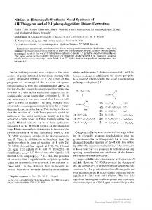
Synthesis of Power-Efficient Memory-Intensive Systems-on-Chip ∗ Darko Kirovski, Chunho Lee, Miodrag Potkonjak Computer Science Department, University of California, Los Angeles, CA, USA William H. Mangione-Smith Department of Electrical Engineering, University of California, Los Angeles, CA, USA
Abstract Recent commercial trends combining computer, personal communication, and commodity electronics have resulted in a new set of system design requirements focusing on power minimization and design reuse. We have developed a new modular synthesis technique for the design of core-based memory-intensive application-specific systems-on-chip optimized for power. The power optimization occurs during hardware-software co-synthesis through compilation and resource allocation. The compilation techniques include reduction of instruction cache misses and placement of frequently executed sequential blocks of code in consecutive Gray code addressed memory locations. The resource allocation technique conducts a search for a near-optimal power-efficient processor and instruction and data cache configuration, while meeting real-time performance demands. In order to bridge the gap between the profiling and modeling tools from two traditionally disjoint synthesis domains (architecture and computer-aided design), we have developed a new synthesis and evaluation platform. The platform integrates the existing modeling, profiling, and simulation tools with system-level synthesis tools. The effectiveness of the synthesis approach is demonstrated on a variety of modern multimedia and communication applications.
Keywords: System-level synthesis, low-power, Gray code addressing, resource allocation, cache power consumption modeling.
∗
A preliminary version of parts of this manuscript has been published at the 1998 Asian and South Pacific Design
Automation Conference, pp. 557-62.
1
1
Introduction
Systems for wireless consumer electronics markets demand design flexibility and large volume data management. The fact that battery performance has not followed the same improvement as the semiconductors technology has established low-power design as the premier design goal for wireless systems [Ben98a]. Similarly, current semiconductor technologies have allowed integration of processors and memory structures on a single die. Therefore, low-power systems-on-chip (SOC) consisting of a programmable processor and memory hierarchy has attracted the attention of virtually all silicon vendors.
Programmable core
Instruction cache
Data cache
Applicationspecific cores
Bridge
CPU on-chip bus
I/O controllers
Bridge System on-chip bus Figure 1: A typical core-based application specific system. Architecture template adopted by the VSI Alliance [VSI98]. An architectural template for modern application-specific SOC, adopted by the VSI Alliance [VSI98], consists of a processor core, instruction and data cache, and a number of optional hardware accelerators and control blocks as depicted in Figure 1. Clearly, the distribution of power dissipation within an application-specific SOC depends on the actual application. However, the microcontroller and/or signal processing core and on-chip caches are likely to dominate SOC power consumption for the next several generations. We have conducted an extensive analysis of on-chip power distribution for a number of state-of-the-art general purpose processors. Product manuals and reference documents indicate that the largest amount of energy in such systems is consumed by the processor and caches [CPU98]. Analytic and experimental results support manufacturers’ data. Gonzalez and Horowitz [Gon96] show in their experiments that 25%-40% of the total energy dissipation of a typical general purpose microprocessor chip is consumed by on-chip caches. Typically, the area (and therefore capacitance) occupied by datapath and memory for state-of-the-art RISC/DSP microprocessors account for approximately 80% of
2
the die area [Dol97]. Similarly, the R3000 processor and on-chip I- and D-caches account for 85% of the overall chip capacitance [Bur94]. Moreover, Burd and Brodersen [Bur96] show that out of 1.2W of total Infopad processor system power dissipation, 120mW and 600mW are due to microprocessor (ARM60) and 512Kb SRAM cache respectively. The Toshiba design team [Nag95] showed that “the cache, the datapath, power and control power are about 50 - 100mW, 100mW - 150mW and 50mW respectively for 3.3V 50MHz operation” of their 150MIPS/W CMOS RISC processor. Finally, Montanaro et al. [Mon96] have found that for a large set of benchmarks 27% of the total power consumption of a designed low-power RISC controller is due the SRAM I-cache accesses.
1.1
Synergic System Synthesis - Program Compilation for Low-Power
Since a significant portion of the overall SOC power consumption comes from the processor and caches, we focus on improving the cache hit ratios, reducing switching activity in the caches, and selecting a system configuration which satisfies the real-time constraints by the target application and achieves lowest overall system power consumption. In addition, the approach can be applied to a set of applications. Two compilation strategies are used to reduce the SOC energy dissipation. The first technique facilitates a global most-constrained least-constraining probabilistic heuristic to minimize the number of I-cache conflicts and therefore reduce the number of off-chip data accesses. Commonly, off-chip memory accesses require one to two orders of magnitude more power dissipation than on-chip memory accesses [Fro97]. Improved cache performance enables scaling down the supply voltage [Cha92]. This change results in larger delays in the system that are acceptable as long as the target application’s timing constraints are satisfied. Cache conflicts are reduced by relocating basic blocks in the executable in such a way that frequently sequentially executed blocks map to different cache lines. The heuristic for performance optimization groups basic blocks into sets, where all blocks in one set map to a single cache line. The second compilation strategy determines which set of blocks is to be assigned to a distinct cache line. This strategy shuffles the sets according to the profiling information of the program execution, so that frequently sequentially executed basic blocks are stored into memory locations with consecutive Gray-code addresses. Thus, the switching activity of the cache decoder, which represents the source of approximately 30% of the overall cache power consumption [Eva95] is minimized for a particular program execution. The overhead of the basic block relocation is injection of jump instructions. As an outer synthesis loop, the resource allocation algorithm performs a search for a power efficient system configuration. The resulting configuration consists of a microprocessor core and I- and D-cache specification (size, associativity and cache line size). The bounded search is guided by evaluating the
3
design trade-offs for the selection of each of the configuration parameters. Sharp lower and upper bounds significantly reduce the number of cache configurations considered for power and performance estimation. This reduction is important because accurate cache performance and power estimation is done using trace-driven simulations. Trace-driven simulation is used to obtain the application execution profile and to count the number of transitions in the cache decoder. The cache model for the assumed 0.5 micron technology is assembled by combining several modeling tools. The cache delay is modeled using the CACTi tool [Wil96]. Cache power dissipation estimation for a particular cache size and organization is based on published experimental results [Eva95, Su95]. The data retrieved from these tools is scaled with respect to actual modern cache implementations [Eva95, Su96, CPU98]. The application profile, latency, and power dissipation models drive an optimization loop which attempts to minimize the system power consumption while meeting the applications’ real-time constraints. In order to bridge the gap between the profiling and modeling tools from the two traditionally independent synthesis domains (architecture and CAD), we have developed a new synthesis and evaluation platform. The platform integrate s the existing modeling, profiling (SHADE [Cme94]) and simulation (DINEROIII [Hill88]) tools with the developed system-level synthesis tools. Application profiles are acquired through the use of SHADE controlled by our own trace analyzer. The result of the trace analysis is an application control flow graph augmented with information on spatial and temporal correlation of branch executions. We evaluate cache subsystem performance by running the DINEROIII cache simulator. The effectiveness of the approach and the constructed simulation and evaluation platform is demonstrated on a variety of modern real-life applications.
2
Related Work
The related work can be traced along the following three lines: system synthesis for low-power applicationspecific systems, processor and memory hierarchy design and energy-efficiency evaluation, and embedded systems compiler design techniques. Systems-on-silicon are becoming an important focus area for both research and commercial developers [Bol94]. Shortened design cycles, due to market pressure, have encouraged the use of predesigned processor cores. At the same time, market pressure to reduce system cost for consumer products has spurred the development of system-level synthesis techniques [DeM97, Chi96, Sub96]. System synthesis techniques have generally focused on task scheduling and resource allocation algorithms [Wol94] governing access for shared resources [Ism96], system design using fixed core interfaces and interface design and verification [Nar94]. Design-for-composability and ease of core synchronization has been addressed
4
at the system and communication level and incorporated into an effective system design framework [Cho98]. In the power optimization domain, various system-level synthesis paradigms for low-power have been proposed [Rab97, Ben97, Lak97], as well as a number of techniques for energy-efficient resource allocation and assignment [Kho98, Li98], along with bus encoding [Ben98b]. The efficacy of some low-power high-level design techniques has been demonstrated on several image and video processing circuits [Cat98, Nac98] and speech encoders [Hen97]. As embedded applications have become more sophisticated, hardware/software co-design has become increasingly important [Gup93, Hen95]. Key optimization problems in hardware/software co-design have been identified as system component allocation, functional partitioning, quality metrics estimation, model refinement [Wil94, Gon97], memory allocation using memory reuse for arrays and storage order [DeG97]. The increased interest in embedded system design with reusable core components has encouraged the development of high-level architecture and ASIC evaluation models. For example, The Microprocessor Report presents a monthly summary of the power dissipation and performance of numerous commercial processor cores [MPR97]. Application-driven microprocessor design, and its performance issues, have been studied by Fisher et al. [Fis96]. Energy efficient microprocessor design has been discussed [Bur96, Gon96]. Instruction and data caches, as the highest level of the memory hierarchy, have been thoroughly studied [Smi83, Hill88, Jou93]. Various memory hierarchy synthesis techniques for multimedia systems have been developed [Fu96]. Cache models for latency [Wil94, Wad92] and power [Ko95, Eva95, Su95] have been developed and power minimization strategies have been evaluated for a number of architectural parameters. Gray code addressing of cache lines has been evaluated by Su and Despain [Su95]. Algorithms that enable efficient Gray code addressing have been developed by a number of researchers [Che97, Vee95, Koe96]. Compiler optimization strategies have been developed for optimizing code generated for embedded systems [Ara95, Lie96]. Compiler directed techniques for minimizing number of cache misses in such studies has received significant attention in the research community. Dynamic address remapping for avoiding conflict misses in large direct-mapped instruction caches has been proposed in [Ber94]. Static code repositioning by using cache line coloring at the procedure or basic block level has been an alternative approach proposed and evaluated by Hwu and Chang and Hashemi et al. [Hwu89, Has97]. Similar technique for profile-driven data repositioning has been proposed by Panda et al. [Pan96].
5
3
Preliminaries
Several factors combine to influence system performance: instruction and data cache miss rates and penalty, processor performance, and system clock speed. Power dissipation of the system is estimated using processor power dissipation per instruction and number of executed instructions per task, supply voltage, energy required for cache read, write, and off-chip data access as well as the profiling information about the number of cache and off-chip accesses. The approach that we use to realistically address power consumption estimation leverages on existing cache and processor models. This enables the synthesis approach to be rapidly updated and applied to environments with new technologies. In this section we describe the hardware performance and energy models for caches and processor cores. Bit lines
DATA ARRAY
DECODER
Address
TAG ARRAY
Word lines
Bit lines
Column muxes Sense amplifiers Comparators Output drivers Mux drivers Data output Output valid
Figure 2: Standard cache implementation [Wil96]. Typical cache design is depicted in Figure 2. The influence of a particular piece of hardware on cache latency is quantified by Wada et al. [Wad92] and more detailed by Wilton and Jouppi [Wil96]. There exists also a number of reports on how energy consumption is distributed among parts of the cache structure. For example, Evans and Franzon show that global decode, precharging, and address latches 6
are responsible for approximately one third of the overall power consumption each [Eva95]. Ko and Balsara conclude that the bit array, address decode, control generator, and sense amplifiers consume in average 40, 18, 25, and 17% respectively of the total power dissipation [Ko94]. Minimal cycle time (ns) Cache size 8B 16B 512B 6.07 5.99 1KB 6.45 6.13 2KB 6.88 6.52 4KB 7.67 7.02 8KB 8.34 7.81 16KB 9.30 8.58 32KB 10.4 9.45
for various direct-mapped caches with variable line sizes 32B 64B 128B 256B 512B 1024B 6.02 6.07 6.23 6.36 6.34 6.51 6.66 6.49 6.56 7.35 7.21 6.99 6.91 7.65 9.40 8.00 7.62 7.54 8.14 9.80 8.91 8.59 8.69 9.30 10.04 10.41
Table 1: Cache latency model is provided by the CACTi tool [Wil96].
Power consumption (nJ) estimation for various direct-mapped caches with variable line sizes (5V) No optimizations Block buffering, sub-banking and Gray code addressing [Su95] Cache size 8B 16B 32B 8B 16B 32B 512B 0.33 0.38 0.47 0.29 0.32 0.40 1KB 0.36 0.39 0.46 0.30 0.30 0.35 2KB 0.42 0.44 0.49 0.32 0.27 0.27 4KB 0.65 0.67 0.69 0.46 0.33 0.27 8KB 1.15 1.15 1.17 0.77 0.50 0.35 16KB 2.16 2.16 2.17 1.41 0.87 0.53 32KB 4.20 4.20 4.21 2.70 1.61 0.92
Table 2: The cache power consumption model is adopted from [Eva95] and [Su94]. We used CACTi [Wil96] as a cache delay estimation tool with respect to the main cache design choices: size, associativity, and line size. The energy model was adopted from published reports [Eva95, Su94]. The overall cache model was scaled with respect to actual industrial implementations. Caches typically found in current embedded systems range from 128B to 32KB. Although larger caches correspond to higher hit rates, their power consumption is proportionally higher, resulting in an interesting design trade-off. Since higher cache associativity results in higher access time, we consider only direct-mapped caches [Kir97]. We have experimented with 2-way set associative. However, they did not dominate in a single case. Cache line size is also variable in our experiments. Its variations 7
correspond to the following trade-off: larger line size results in higher cache miss penalty delay and higher power consumption by the sense amplifiers and column decoders; smaller line size results in large cache decoder power consumption. Extreme values result in significantly increased access time. We estimated the cache miss penalty based on the operating frequency of the system and external bus width and clock for each system investigated. This penalty ranged between 4 and 20 system clock cycles. Writeback was adopted rather than write-through, as it provides superior performance and power savings in uniprocessor systems [Jou93] though at increased hardware cost. Each of the processors considered was constrained by the Flynn limit, and is able to issue at most a single instruction per clock period. As a consequence, caches were designed to have a single access port. Microprocessor core StrongARM ARM, 7 ARM, 7 Low-Power LSI Logic, TR4101 LSI Logic, CW4001 LSI Logic, CW4011 DSP Group, Oak NEC, R4100 Toshiba, R3900 Motorola, 68000 PowerPC, 403 ARM 710 (ARM7 / 8KB) SA-110 (StrongARM / 32KB)
Clock (MHz) 233 40 27 81 60 80 80 40 50 33 33 40 200
MIPS 266 36 24 30 53 120 80 40 50 16 41 72 230
Technology (µm) 0.35 0.6 0.6 0.35 0.5 0.5 0.6 0.35 0.6 0.5 0.5 0.6 0.35
Area (mm2 ) 4.3 5.9 3.8 2 3.5 7 8.4 5.4 15 4.4 7.5 34 50
Power diss. (mW ) (Voltage) 300 (1.65) 200 (5) 45 (3.3) 81 (3.3) 120 (3.3) 280 (3.3) 190 (5) 120 (3.3) 400 (3.3) 35 (3.3) 40 (3.3) 424 (5) 900 (1.65)
Table 3: Processor performance and power consumption models used in the experimentations. A sample of the cache model data is given in Tables 1 and 2. Cache access delay and power consumption model were computed for a number of organizations and sizes, assuming feature size of 0.5 µm and typical six transistors per CMOS SRAM cell implementation. We adopted 98nJ as the nominal energy consumption per single off-chip memory access [Fro97]. Data on microprocessor cores was extracted from manufacturer’s datasheets as well as from the CPU Center Info web site [CPU98]. A sample of the collected data is presented in Table 3. The table presents embedded microprocessor core operating frequency, MIPS performance, technology, area, and nominal power consumption. The last two rows of the table show two integrated microprocessor products with on-chip caches and their system performance data. We use voltage scaling as a powerful power consumption minimization strategy during synthesis. 8
The supply voltage Vdd vs. delay TD model used in the experimentations was quantified by the following formula: TD = K ·
4
Vdd , (Vdd −Vt )2
where K is constant [Cha92].
The Global Flow of the System-Level Synthesis Approach
Figure 3 illustrates the modular synthesis system. In this section we describe the function of each module and how they are combined into a tightly coupled optimizing and synthesis system. Search for minimal power consumption multiple application targeted Processor, I-Cache and D-Cache Configuration
I-Cache
Control flow graphs, profile data
Processor
D-Cache
Performance and power optimization heursitic for mapping basic blocks to I-Cache lines
System Performance and Power Consumption Estimation
PERFORMANCE SIMULATION
Applications
Input data
Figure 3: The hierarchical modular synthesis approach. The core of the synthesis flow is the global most-constrained least-constraining heuristic for basic block relocation. Basic blocks are repositioned statically in such a way that frequently sequentially executed basic blocks are mapped into different cache lines. Furthermore, the mappings are shuffled so that the switching activity in the I-cache decoder is minimized for a particular execution of the target application. Code repositioning is accomplished with negligible increase in the static program memory size. The modification required to the program involves basic block motion, branch target updating, and branch insertion. The application-driven search for a low-power core and cache system requires usage of trace-driven cache simulation for each promising point (instruction and data cache) space. Since trace-driven cache simulation can be an expensive operation, we opt to use search algorithms that carefully scan the design space using conservative sharp lower and upper bounds and by providing powerful algorithmic performance and power estimation techniques. 9
Our synthesis tools are augmented with the ability to synthesize a single-chip programmable applicationspecific system which satisfies the requirements of multiple applications. This system requirement represents a realistic design scenario for most modern non-preemptive multitask application-specific systems (e.g. speech compression and activity detection, signal encoding, etc.). The synthesis technique considers each non-dominated microprocessor core and competitive cache configuration, and selects the implementation which requires minimal power consumption and satisfies the individual performance requirements of all target applications. System performance is evaluated using a platform which integrates simulation, modeling, and profiling tools as shown in Figure 4. SHADE is a tracing tool which allows users to define custom trace analyzers and thus collect rich information on runtime events. SHADE currently profiles only SPARC binaries. The executable binary program is dynamically translated into host machine code. The tool also provides a stream of data to the translated code which is directly executed to simulate and trace the original application code. A custom analyzer composed of approximately 2,500 lines of C code, is linked to SHADE to control and analyze the generated trace information. The analyzer reads relevant trace information from SHADE and builds a control flow graph (CFG) corresponding to the dynamically executed code. The analysis consists of two passes: the first pass determines the boundaries of basic blocks, while the second pass constructs a CFG by adding control flow information between basic blocks. We collect the frequencies of control transfers through each basic block and information on branch temporal correlation [Kir97b]. Table 4 shows a typical CFG generated by the analyzer. The first two columns show the basic block starting and ending address. Branch type (conditional[1], unconditional[2], procedure call[4], or indirect branch target jmpl[3]) and the number of possible target addresses appear in the next two columns. The target address, and the number of control transfers to it (activations) are given for both targets in next four columns. The temporal correlation of branch activations and size of the appropriate basic block (in bytes) are shown in the last two columns. Once the CFG is obtained, an algorithm is employed to reposition application basic blocks in such a way that instruction cache misses and cache decoder switching activity are minimized. We use a basic block relocation table to simulate the relocation in main memory. An entry in the basic block relocation table consists of two elements: the original and optimized starting address of the basic block. To simulate cache performance of a given application and data stream, we use a trace-driven cache simulator DINEROIII. The cache is described using a number of qualitative and quantitative parameters such as instruction and data cache size, replacement policy, associativity, etc. The system optimization process is composed of a sequence of activations of each of these tools. The SHADE analyzer traces program and data memory references and constructs the CFG. The CFG 10
is used to drive the code reposition module which produces a new application mapping table. Stream of references are sent to a program that uses the basic block relocation look-up table to map from the original address space into the optimized address space. The remapped trace of addresses, along with all unmodified data memory references, is sent to DINEROIII for cache simulation.
ANALYZER
Trace
User programmed
Application [executable binary]
SHADE Binary translation
Input data
Control Flow Graph Profile Information
A 31
22
B
C
Trace, Basic Block addresses...
Control Flow Graph Partitioning Power and performance optimization heuristics
I-Cache and D-Cache Descriptions Feature size, # I/O ports, Bus size, Cache Size, Line size, Associativity, Replacement and write hit policies
Instruction and data access trace
Basic Block relocation table Address Original 0 40 120 ...
Address Optimized 20 80 600 ...
optimized application trace
CPU and Cache Modeling Tools Power estimation & max clock speed
non-optimized application trace
DINERO - Cache Simulator Cache performance evaluation
Cache and processor core model
Cache misses
Performance and power consumption METER
System’s operational voltage supply
Figure 4: Synthesis flow of application-driven programmable core-based systems. The final system performance is computed using the following formula: CyclesP erInstruction = SystemClockF requency M IP S
+ (I − CacheM issRatio + D − CacheM issRatio) · CacheM issP enalty
{I, D} − CacheM issRatio was computed during the trace driven simulation of the cache subsystem. 11
CacheM issP enalty, SystemClockF requency, and M IP S are system parameters introduced in Section 3. The system power consumption was computed using the following formula: SysP owCons = ((T C − CP U IC) · CP U EP C + CA · EP CA + M A · EP M A) · Scale(V oltageSupply) where T C is the total number of cycles required to execute the application, CP U IC is the number of cycles while the CPU is idle waiting for data to be fetched from main memory to cache (blocking caches assumed due to lower hardware cost), CP U EP C is the average energy per cycle for a particular processor core, CA and EP CA are the number of cache accesses and energy consumed per access respectively, and M A and EP M A are the number of main memory accesses (reads due to cache misses and writeback updates) and energy consumed per memory access respectively. Function Scale(V oltageSupply) returns the scaling factor for V oltageSupply with respect to the nominal supply voltage (3.3V). The computed energy consumption is scaled due to the difference between the supplied voltage and the nominal voltage used for power evaluation of all denoted parameters. The power savings due to decreased transitions in the cache decoder are encountered by scaling down 30% of the total cache power consumption with the ratio of the number of transitions due address change in the optimized (relocated) and traditional basic block schedule.
Start 10074 10098 100a8 100b0 100e8 100f8
Branch Stop Type 1008c [1] 100a4 [4] 100ac [4] 100d4 [4] 100f0 [4] 10118 [1]
Targets 2 2 2 2 2 2
T1 address 10098 100a8 100b0 100e8 100f8 1012c
Targets T1 taken T2 address 04532 101aa 04527 1032a 04520 101fc 02300 10fa4 02247 10182 01012 10160
T2 taken 00005 00007 02220 00053 01235 00324
TempCorr 0.999 0.999 0.824 0.991 0.923 0.183
Size 28 16 8 40 12 36
Table 4: Analyzer output format.
5
Synthesis Algorithms
The problems encountered in the synthesis of a low-power SOC, and associated optimization algorithms, are described in the following subsections. First, the algorithm for basic block relocation for low-power is discussed. Then, based on the obtained code repositioning and hence, improved cache performance, we assemble a power-efficient system configuration (core and cache structure) which satisfies performance requirements specific to a set of target applications.
12
5.1
Application to Cache Mapping for Low-Power
The core of the proposed application-driven system-level synthesis technique involves basic block repositioning based upon profile information. Basic block repositioning is undertaken in two phases. In the first phase the relocation aims for application execution on fixed hardware resources with minimal number of cache misses. The second phase relocates the part of code assigned to a particular cache line to a set of addresses which map to the same cache entry in a way that basic blocks frequently executed sequentially are stored at consecutive Gray code locations. 0
1 1
1
0
2 3
2
6
3
600/0
7
5
3
300 100
4 5
200
4
6
6
New
5
7 Partitions of basic blocks mapped to the same cache line (8). Program size < 67 cache lines. Not all edges are drawn.
Graph which describes the frequencies of accessing a block in one partition followed with a block from another. The graph is directed - e.g. the bold edge represents two edges with corresponding weights: 600 times after basic block in partition ONE is executed the next basic block is in partition SIX, and 0[6->1].
Node merging - nodes 1, 3, 5, and 6 are merged into node NEW.
Figure 5: Modeling the problem of encoding partitions of basic blocks which map to the same cache line. The first phase in the relocation strategy is described in detail by Kirovski et al. [Kir97]. The collected run-time information on the execution of the program is used to generate and weight a CFG. The profile information quantifies the spatial and temporal dependencies for each resolution of a branch. Using this data, the CFG of the program is annotated so that spatially and temporally correlated basic blocks are identified. Once the CFG is transformed, basic blocks are partitioned into N sets, where each set corresponds to a cache line. The cache structure contains exactly N entries (cache lines). The goal of the partitioning function is to minimize the sum of weights between partitions. This goal results in overall reduction of instruction cache misses, i.e. basic blocks that are likely to be executed 13
sequentially are mapped into memory locations which correspond to disjoint cache lines. Since the problem of finding the optimal basic block mapping is computationally intractable [Gar79], we opted to employ the heuristic presented by Kirovski et al. [Kir97]. After partitions of basic blocks are identified, in the second phase of the optimization strategy, we assign these partitions to particular cache lines (addresses, entries). As shown in Figure 5, this problem is modeled using a graph representation. Each partition of basic blocks, selected to map to one cache line, is represented as a node in the graph. The weight of a directed edge between two nodes (partitions) A (source) and B (destination) is computed as a sum of weights of all edges in the original CFG that have a basic block BBA ∈ A as a source and basic block BBB ∈ B as a destination. There may exist two edges of opposite directions between two nodes. Since the number of nodes corresponds to the number of entries in the cache structure, the goal of the optimization algorithm is to assign entries to nodes in such a way that the sum of products of the Hamming distance and weights between two nodes is minimal. The problem of embedding a general weighted graph, to minimize the weighted lengths, in an n-dimensional cube is NP-hard [Afr85]. To date, a number of effective algorithms which address this optimization problem has been devised [Che97, Vee95, Koe96]. Function EncodeSubsetofNodes(Graph G) V ertices times Repeat SubsetCardinality Randomly select a subset S of SubsetCardinality vertices Compute its objective function as: P ObjF unc(S) = P
Vi ∈S
EVi ,Vi+1
(EV,W ·Hamming(V,W )) V ∈S,W ∈S /
where Hamming(V, W ) returns the Hamming distance between nodes V and W . If node W has not been assigned an address, Hamming(V, W ) returns one. Repeat K times Select two random nodes V in and W outside the current subset. Replace V with W . Update the objective function for the current subset. End Repeat Select the ordered subset S + with the greatest objective function value and assign SubsetCardinality successive Gray-code addresses to the vertices in S + . in the order of their selection. End Repeat Merge all nodes in each subset into one node. The incoming edges into the starting and outgoing edges from the ending vertex in the parent subset the subset remain existing in the new graph G∗ . If Cardinality(G∗ ) < M → SolveExact(G∗ ) else EncodeSubsetofNodes(Graph G∗ )
Figure 6: Pseudo-code for the encoding assignment procedure.
14
We have developed a novel probabilistic most-constrained least-constraining heuristic for state encoding that targets reduced switching. The heuristic is explained in detail using the pseudo-code presented in Figure 6. The algorithm leverages the advantages of a number of algorithm development and implementation techniques: • Iterative design space reduction. The algorithm iteratively performs a search for a subset of nodes which satisfies the mostconstrained least-constraining heuristic objective function and assigns encodings to this set of nodes. These two steps are repeated until all nodes in the graph are not assigned a unique encoding. • Random search using locally computed objective function. The algorithm performs a random search for an ordered subset of nodes in the graph which has the highest value for the objective function that guides the heuristic. The objective function (see Figure 6) takes into account the constraints of each node in the subset. It forces early selection of a subset of vertices which has the highest sum of edge weights (most-constrained vertices) and smallest sum of edges connecting two nodes, one in, and the other outside the subset (leastconstraining remainder of the problem space). The edges are summed corresponding to their order in the subset. The cardinality of the subset is equal to a number which is a power of two. Subset cardinality and the number of iterations in the randomized search for each objective-efficient subset are parameters of the heuristic implementation. The next subset candidate is generated from the current one by performing a local random node exclusion and inclusion from/to the list of nodes in the subset. This technique enables computationally inexpensive update rather than recomputation of the objective function for the succeeding subset candidate. Due to its low computation requirements this approach boosts the performance of the algorithm by enabling the generation of a large set of candidates. Once the subset is selected it is assigned a set of consecutive Gray-code addresses and removed from the list of vertices considered for further subset selection. However, the vertices are not removed from the graph. The assigned encodings are used to add another component to the objective function described above. The objective function of an ordered subset is now scaled with the factor of how the subset fits the existing encoding assignments (see pseudo-code in Figure 6). When all subsets are selected, the graph is transformed so that all nodes in one subset are merged into a single vertex (see Figure 5). This vertex inherits only the incoming edges of the initial and outgoing edges of the ending vertex of the parent subset. In the next iteration of the algorithm, although the graph is reduced in size, the goal of the optimization strategy remains the same. 15
• Pool of intermediate solutions. While generating the subset candidates, the algorithm maintains a list of K most objective-efficient subsets. After a predefined number of candidates is generated, a local search for more objectiveefficient subset is performed with subsets from the list of currently best solutions as a starting point. • Search time management. Since it is considerably harder to find good subset candidates at the beginning of the search (because of the larger problem space), we distribute the time allocated for selection and encoding of one subset of nodes according to the difficulty of finding a good candidate. In our experiments we used a curve inversely exponentially proportional to the number of nodes in the graph to manage the search time at each step in the algorithm.
5.2
Resource Allocation for Low-Power
In this phase of the synthesis approach, a search is conducted for a energy-efficient system configuration and its voltage supply value which satisfy the performance requirements of the set of target applications. The search algorithm is described using the pseudo-code shown in Figure 8. Figure 7 demonstrates how competitive hardware configurations are traced for the optimal solution. The search algorithm evaluates number of cache systems and uses a technique to reduce the search space of competitive processor-cache systems from a continuous to discrete domain. Since performance and power evaluation of a single processor, I- and D-cache configuration require trace-driven simulation, the goal of our search technique is to reduce the number of evaluated cache systems using sharp lower and upper bounds for cache system performance and power estimations. However, a particular cache system is evaluated using trace-driven simulation only once since the data retrieved from such simulation can be used for overall system power consumption estimation for different embedded processor cores with minor additional computational expenses. The search algorithm, as a preprocessing step, excludes from further consideration processors dominated by other processor cores. One processor type dominates another if it consumes less power at higher frequency and results in higher MIPS performance at the same nominal power supply. The competitive processors are then sorted in ascending order with respect to their power consumption per instruction and frequency ratio. Microprocessors which seem to be more power-efficient are given priority in the search process. This step results in later on sharper bounds for search termination. Finally, at the nominal supply voltage power consumption is estimated for the most power-efficient processor combined with all cache configurations which satisfy the performance requirements of all target applications (see 16
Figure 7; point A). The search for the most efficient cache configuration is bounded with conservative sharp lower and upper bounds. The sharp upper bound on cache increase for fixed voltage supply and processor core is determined by measuring the number of conflict misses and comparing the energy required to fetch the data from off-chip memory due measured conflict misses and the power that would have been consumed for twice as large cache and same number of cache accesses (number of cache conflicts assumed to be zero). In the former case we terminate further increase of the particular cache structure. Similarly, the lower bound is defined at the point when the energy required to fetch the data from off-chip memory due conflict cache misses for twice smaller cache with zero-energy consumed per cache access is larger than the energy required for both fetching data from cache and off-chip memory in the case of the larger cache structure. The smallest cache system which meets the performance requirements of the set of target applications guarantees power consumption optimality for fixed microprocessor and fixed supply voltage (Figure 7; point A; configuration CP U 1, I$1, D$1).
Power consumption of the system configuration
CPU6, I$1, D$1
Min Power
CPU5, I$2, D$2 CPU4, I$1, D$2 CPU2, I$2, D$1
CPU3, I$1, D$1
E
D
C
CPU1, I$1, D$1
Voltage Supply B
A
Figure 7: An example of exhaustive search for the power-optimal hardware configuration.
17
The result of evaluation of all competitive hardware configurations is a cache-processor configuration that represents the power-optimal solution at the nominal voltage supply (in our experiments we used 3.3V). Now, the voltage supply can be reduced to the point where the current best configuration does barely meet the applications’ timing constraints. The key step in the search mechanism is the translation of the search domain for the voltage supply from a continuous into a discrete domain. As shown in Figure 7, the curves that represent power consumption behavior for a single system configuration are congruent with respect to the voltage supply change. This means that a configuration which gives the best energy savings for a specific voltage continuously has the best results in the domain of its definition, i.e. until able to satisfy the application constraints. Accordingly, we compare hardware configurations only at the discrete points of discontinuity of curves which quantify configurations’ power analysis. In the example in Figure 7, the point of discontinuity of the configuration, selected at point A, is at point B. Point B represents the first solution (configuration and voltage) candidate. V oltageSupply = 3.3V erInstruction ) Sort processor cores in a list L according to min( EnergyP F requency Delete the dominated processor cores from L Repeat For I-cache = 512B..32KB and CacheLineSize = 8B..512B For D-cache = 512B..32KB and CacheLineSize = 8B..512B Check upper, lower bounds; if exceeded break; If (I- and D-cache configuration has never been evaluated) Evaluate power consumption of the cache structure According to the existing cache system analysis evaluate the power consumption of the entire system (with the processor core) Memorize Configuration C if power consumption is minimal End For End For Scale down the V oltageSupply until C does not satisfy application constraints. Delete the processor core P C ∈ C from the list of cores L until L is not empty.
Figure 8: Pseudo-code for the resource allocation procedure. In order to search for a configuration which results in lower power consumption at point B, we estimate the power characteristics of all application-feasible configurations (which do not have the same processor core as the first configuration candidate) and select the one with the best performance (CP U 2, I$2, D$1). However, since we already have the current best solution (from previous processor core evaluations, CP U 1, I$1, D$1) the bounds are now even sharper. Namely, we set the final upper and lower bound on the cache structure size and organization as follows: 18
• Upper bound. Given: Feasible cache structure (I- and D-cache), and processor core A. We terminate further increase of the cache structure when the increase of the power consumption due larger cache (although cache conflicts total zero) would be larger than the energy consumed by the current best solution. • Lower bound. Given: Feasible cache structure (I- and D-cache), and processor core A. We abort further decrease of the cache structure if the amount of energy required to bring the data due additional cache misses from off-chip memory (although the smaller cache power consumption totals zero) is larger than the energy consumed by the current best solution. The algorithm iterates the process of scaling down the voltage supply of the current best configuration until it can: • barely satisfy the deadlines, • find better configurations which operate at the same voltage but with different processor core. The iterative search is performed until the last application-feasible processor core configuration is evaluated for power. This configuration has the ability to satisfy the application constraints at the lowest voltage supply (point E; configuration CP U 6, I$1, D$1). However, this property does not guarantee the best overall power savings. For example, in Figure 7, the most power-efficient configuration found is CP U 3, I$1, D$1 at point D.
6
Experimental Results
In this section, we present a report on the conducted experiments. First, we describe the benchmarks and its input data used for the evaluation of our approach. We used nine applications, shown in Table 5 to demonstrate the effectiveness of the approach [Lee97]. A brief description of data files of the benchmarks are given in Table 6. All nine applications are in public domain and can be obtained via the Internet. JPEG software from the Independent JPEG Group implements JPEG baseline, extended-sequential, and progressive compression processes. We used integer DCT for decoding a JPEG file to a PPM file. Integer DCT and progressive compression process options were used for compression. GSM software used in the experiment is an implementation of the European GSM 06.10 provisional standard for full-rate speech transcoding, prI-ETS 300 036, which uses RPE/LTP (residual pulse excitation/long term prediction) coding at 13 kbit/s. A 16-bit linear PCM data file is used to measure
19
execution parameters of the GSM encoder. The measurement of the GSM decoder execution characteristics was done using the output of the GSM encoder. EPIC (Efficient Pyramid Image Coder) implements lossy image compression and decompression utilities. The compression algorithm is based on a critically-sampled (imperfect-reconstruction) dyadic wavelet decomposition and a combined runlength/Huffman entropy coder. The remaining benchmarks (Mipmap, Osdemo, and Texgen) use a 3-D graphic library called Mesa. The author of the library claims that Mesa is a compliant implementation of OpenGL since it uses the OpenGL API. Mipmap is a simple mipmap texture mapping example. Osdemo is a demo program that draws a set of simple polygons using the Mesa 3-D rendering pipe. Finally, Texgen renders a texture mapped version of the Utah teapot. Application JPEG encoder JPEG decoder GSM encoder GSM decoder EPIC encoder EPIC decoder Mipmap Osdemo Texgen
Source Independent JPEG Group Technische Universit¨at, Berlin University of Pennsylvania University of Wisconsin
Description JPEG image encoding/decoding European wireless voice coding standard Wavelet image encoding/decoding 3-D rendering examples using Mesa graphics library
Table 5: A brief description of applications used in the experiments.
Benchmark JPEG encoding JPEG decoding GSM encoding GSM decoding EPIC encoding EPIC decoding Mipmap Osdemo Texgen
File size Format 101,484 bytes PPM 5,756 bytes JPG 295,040 bytes 16 bit PCM 30,426 bytes GSM encoded 65,595 bytes PGM 7,432 bytes EPIC encoded N/A N/A N/A
Description an uncompressed bit map a JPEG compressed Clinton speech Clinton speech Gray scale 256 × 256 Gray scale 256 × 256 mipmap texture mapping example 3-D rendering pipeline example texture mapped Utah teapot
Table 6: A brief description of data used in the experiments. The performance of the synthesis approach has been quantified using the described applications, the input data, and the hard real-time constraints as shown in Table 7. The upper part of the table 20
presents the configurations which were found to be the most power-effective for a particular benchmark. For each application and its timing constraint the champion configuration is described by specifying its processor type, the associated I- and D-cache structures (cache sizes followed by cache line size). These properties of the system are shown in columns three, four, and five of the table. The sixth column quantifies the power dissipation of the system for execution of one iteration of the application. The last seventh column points to the percentage improvement with respect to the average configuration among all the configurations minimal at the discrete points of system evaluation (see Figure 7; for example, for points A, B, C, D, and E, the “average configuration “ is configuration at point C with CP U 2 as a processor core). The performance of the “average” configurations is presented in the lower part of Table 7.
Application JPEG encoding JPEG decoding EPIC MipMap OSDemo TexGen GSM encoding UnEPIC GSM decoding
Deadline 1.8 sec 0.08 sec 1.0 sec 0.85 sec 0.35 sec 1.0 sec 3.5 sec 0.33 sec 0.3 sec
Application JPEG encoding JPEG decoding EPIC MipMap OSDemo TexGen GSM encoding UnEPIC GSM decoding
Deadline 1.8 sec 0.08 sec 1.0 sec 0.85 sec 0.35 sec 1.0 sec 3.5 sec 0.33 sec 0.3 sec
Our synthesis approach CPU I-Cache D-Cache Motorola 68000 1KB/64B 2KB/64B LSI TR4101 1KB/128B 4KB/64B LSI TR4101 512B/64B 4KB/64B LSI TR4101 512B/32B 4KB/32B LSI CW4001 1KB/64B 2KB/32B LSI TR4101 1KB/64B 16KB/32B Motorola 68000 1KB/128B 2KB/64B LSI CW4001 1KB/64B 4KB/64b PowerPC 403 512B/64B 1KB/128B Average minimal configuration CPU I-Cache D-Cache ARM 7 LPower 512B/64B 1KB/64B LSI TR4101 512B/32B 4KB/64B LSI TR4101 512B/32B 4KB/64B ARM 7 LPower 512B/64B 2KB/128B LSI TR4101 512B/64B 1KB/64B PowerPC 403 1KB/32B 1KB/128B LSI TR4101 1KB/64B 1KB/64B LSI TR4101 512B/64B 512B/32B Motorola 68000 512B/32B 512B/128B
Energy 8.93041e+06 3.13734e+06 3.39034e+07 4.92554e+07 7.35758e+06 1.2257e+08 1.01969e+08 5.88138e+06 1.00394e+10
Improvement 8% 31% 32% 243% 11% 464% 21% 14% 35%
Energy 9.66097e+06 4.10338e+06 4.45923e+07 1.11614e+10 8.16397e+06 5.70084e+08 1.22567e+08 6.68748e+06 1.3567e+10
Table 7: Experimental results: comparison of our synthesis approach to the power consumption performance of an average configuration that satisfies the timing constraints. The approach results in quantitatively diverse improvements depending on the actual applications and imposed timing constraints. We opted to test the approach for strict as well as relaxed deadlines for our system. Such selection of constraints resulted in improvements over the “average” competitive configuration candidate in the range from 8% to 464%. The highest improvements in the power dissipation occurred in cases where the number of cache misses was substantially reduced using the basic block relocation compilation technique [Kir97]. In addition, in the two extreme cases where energy 21
savings were 243% and 464%, the tight timing constraints forced selection of fast, but energy-expensive processor cores in the “average configuration”, while the power and cache miss optimizations enabled leveraging the power consumption advantages of more energy-efficient processor architectures. The heuristic used to minimize the transitions in the cache decoder resulted in further 35% reduction in power dissipation in the I-cache decoder with negligible standard deviation. The percentage of power dissipation of the overall system due the I-cache accesses ranged from 21% (JPEG decoding) to 44% (TexGen). Finally, the synthesis approach is computationally expensive due to extensive trace-driven simulations. For example, the search for the most power-efficient configuration for JPEG encoding took 10 hours on a SPARC Ultra 5 workstation. Nevertheless, the deployed lower and upper bounds in the solution space search substantially reduced the number of investigated cache structures.
7
Conclusion
We have developed algorithms for system-level power reduction of instruction cache misses, instruction and data cache size and organization selection, placement of frequently executed sequential basic blocks of code in consecutive Gray code addressed memory locations, and power-efficient processor and cache matching with the applications. The compilation performance and power optimization algorithms enable effective synthesis of core-based low-power systems-on-chip. The new synthesis platform integrates the existing modeling, profiling, and simulation tools with the developed system-level synthesis tools. The effectiveness of the approach is demonstrated on a variety of modern industrial-strength multimedia and communication applications, such as MPEG and JPEG encoders and decoders.
References [Afr85] F. Afrati, C. H. Papadimitriou, and G. Papageorgiou. The complexity of Cubical Graphs. Information and Control, vol.66, pp. 53-60, 1985. [Ara95] G. Araujo and S. Malik. Optimal code generation for embedded memory non-homogeneous register architectures. International Symposium on System Synthesis, pp. 36-41, 1995. [Ben97] L. Benini, G. De Micheli, E. Macii, M. Poncino, et al. System-level power optimization of special purpose applications: the Beach Solution. International Symposium on Low Power Electronics and Design, pp.24-9, 1997. [Ben98a] H.-B. Bengtsson. Intelligent management optimises battery life. Electronic Product Design, (suppl.issue), IML Techpress, pp.93-4,96, 1998. [Ben98b] L. Benini, G. De Micheli, E. Macii, D. Sciuto, et al. Address bus encoding techniques for system-level power optimization. Design, Automation and Test in Europe, pp.861-6, 1998. [Ber94] B.N. Bershad, D. Lee, T.H. Romer, and J.B. Chen. Avoiding conflict misses dynamically in large direct-mapped caches. International Conference on Architectural Support for Programming Languages and Operating Systems, vol.29, (no.11), pp.158-70, 1994.
22
[Bol94] I. Bolsens, K. Rompaey, and H. De Man. User requirements for designing complex systems on silicon. VLSI Signal Processing VII, pp.63-72, 1994. [Bur94] T.D. Burd and R.W. Brodersen. Energy efficient CMOS microprocessor design. Hawaii International Conference on System Sciences, pp.288-297, 1995. [Bur96] T.D. Burd and R.W. Brodersen. Processor design for portable systems. Journal of VLSI Signal Processing, vol.13, (no.2-3), pp.203-221, 1996. [CPU98] http://infopad.eecs.berkeley.edu/CIC/ [Cat98] F. Catthoor, M. Janssen, L. Nachtergaele, and H. de Man. System-level data-flow transformation exploration and power-area trade-offs demonstrated on video codecs. Journal of VLSI Signal Processing Systems for Signal, Image, and Video Technology, vol.18, (no.1), pp.39-50, 1998. [Cha92] A.P. Chandrakasan, S. Sheng, and R.W. Brodersen. Low-power cmos digital design. IEEE Journal of Solid-State Circuits, vol.27, (no.4), pp.473-484, 1992. [Che97] De-Sheng Chen and M. Sarrafzadeh. Cube-embedding based state encoding for low power design. ASP-DAC, pp. 613-618, 1997. [Chi96] M. Chiodo, D. Engels, P. Giusto, H. Hsieh, A. Jurecska, L. Lavagno, K. Suzuki, and A. Sangiovanni-Vincentelli. A case study in computer-aided co-design of embedded controllers. Design Automation for Embedded Systems, vol.1, (no.1-2), pp. 51-67, 1996. [Cho98] P. Chou and G. Borriello. Modal Processes: Towards Enhanced Retargetability Through Control Composition of Distributed Embedded Systems. Design Automation Conference, 1998. [Cme94] B. Cmelik and D. Keppel. Shade: a fast instruction-set simulator for execution profiling. SIGMETRICS Conference on Measurement and Modeling of Computer Systems, vol.22, (no.1), pp. 128-37, 1994. [DeG97] E. De Greef, F. Catthoor, and H. De Man. Memory size reduction through storage order optimization for embedded parallel multimedia applications. Parallel Computing, vol.23, (no.12), pp.1811-37, 1997. [DeM97] G. De Michelli and R.K. Gupta. Hardware/software co-design. Proceedings of the IEEE, vol.85, (no.3), pp.349-65, 1997. [Dol97] M. Dolle, S. Jhand, W. Lehner, O. Muller, et al. A 32-b RISC/DSP microprocessor with reduced complexity. IEEE Journal of Solid-State Circuits, vol.32, (no.7), pp.1056-1066, 1997. [Eva95] R.J. Evans and P.D. Franzon. Energy consumption modeling and optimization for SRAMs. IEEE Journal of Solid-State Circuits, vol.30, (no.5), pp.571-579, 1995. [Fis96] J.A. Fisher, P. Faraboschi, and G. Desoli. Custom-fit processors: letting applications define architectures. MICRO-29, pp. 324-335, 1996. [Fly96] M.J. Flynn. Computer Architecture: Pipelined and Parallel Processor Design. Jones and Bartlett, Boston, MA, 1996. (http://umunhum.Stanford.EDU/tools/cachetools.html) [Fro97] R. Fromm, S. Perissakis, N. Cardwell, C. Kozyrakis et al. The energy efficiency of IRAM architectures. International Symposium on Computer Architecture, vol.25, (no.2), pp. 327-337, 1997. [Fu96] S.T. Fu, D.F. Zucker, and M.J. Flynn. Memory hierarchy synthesis of a multimedia embedded processor. International Conference on Computer Design, pp. 176-184, 1996.
23
[Gar79] M.R. Garey and D.S. Johnson. Computers and intractability: a guide to the theory of NP-completeness. W. H. Freeman, San Francisco, CA, 1979. [Gon96] R. Gonzalez and M. Horowitz. Energy dissipation in general purpose microprocessors. IEEE Journal of Solid-State Circuits, vol.31, (no.9), pp. 1277-1284, 1996. [Gon97] Jie Gong, D.D. Gajski, and S. Bakshi. Model refinement for hardware-software codesign. Transactions on Design Automation of Electronic Systems, vol.2, (no.1), pp.22-41, 1997. [Gup93] R.K. Gupta and G. De Micheli. Hardware-software cosynthesis for digital systems. IEEE Design and Test of Computers, vol.10, (no.7), pp. 29-41, 1993. [Has97] A.H. Hashemi, D.R. Kaeli, and B. Calder. Efficient procedure mapping using cache line coloring. SIGPLAN Notices, vol.32, (no.5), pp.171-82, 1997. [Hen95] J. Henkel and R. Ernst. A path-based technique for estimating hardware runtime in HW/SW-cosynthesis. International Symposium on System Synthesis, pp. 116-121, 1995. [Hen97] R.E. Henning and C. Chakrabarti. High-level design synthesis of a low power, VLIW processor for the IS-54 VSELP speech encoder. International Conference on Computer Design, pp.571-6, 1997. [Hill88] M.D. Hill. A case for direct-mapped cache. IEEE Computer, pp. 25-40, 1988. [Hwu89] W.W Hwu and P.P Chang. Achieving high instruction cache performance with an optimizing compiler. International Symposium on Computer Architecture, pp. 242-251, 1989. [Ism96] T.B. Ismail, J.-M. Daveau, K. OBrien, and A.A. Jerraya.
A system-level communication synthesis approach for hard-
ware/software systems. Microprocessors and Microsystems, vol.20, (no.3), pp.149-57, 1996. [Jou93] N.P. Jouppi. Cache write policies and performance. International Symposium on Computer Architecture, vol.21, (no.2), pp. 191-201, 1993. [Kho98] K.S. Khouri, G. Lakshminarayana, and N.K. Jha. IMPACT: A high-level synthesis system for low power control-flow intensive circuits. Design, Automation and Test, pp.848-54, 1998. [Kir97] D. Kirovski, C. Lee, M. Potkonjak, and W. Mangione-Smith. Application-driven synthesis of core-based systems. International Conference Computer Aided Design, pp.104-7, 1997. [Ko95] U. Ko and P.T. Balsara. Characterization and design of a low-power, high-performance cache architecture. International Symposium on VLSI Technology, Systems, and Applications, pp. 235-238, 1995. [Koe96] M. Koegst, G. Franke, and K. Feske. State assignment for FSM low power design. EURO-DAC 96, pp. 28-33. [Lak97] G. Lakshminarayana, A. Raghunathan, N.K. Jha, and S. Dey. A power management methodology for high-level synthesis. International Conference on VLSI Design, pp. 24-9, 1997. [Li98 Yanbing Li and J. Henkel. A Framework for Estimating and Minimizing Energy Dissipation of Embedded HW/SW Systems. Design Automation Conference, 1998. [Lie96] C. Liem, P. Paulin, and A. Jerraya. Address calculation for retargetable compilation and exploration of instruction-set architectures. Design Automation Conference, pp.61-77, 1996. [MPR97] Microprocessor Report, all isues, 1997.
24
[Mon96] J. Montanaro, et al. A 160-MHz, 32-b, 0.5-W CMOS RISC microprocessor. IEEE Journal of Solid-State Circuits, vol.31, (no.11), pp.1703-1714, 1996. [Nac98] L. Nachtergaele, D. Moolenaar, B. Vanhoof, F. Catthoor, et al. System-level power optimization of video codecs on embedded cores: a systematic approach. Journal of VLSI Signal Processing Systems for Signal, Image, and Video Technology, vol.18, (no.2), pp.89-109, 1998. [Nag95] M. Nagamatsu, et al. A 150 MIPS/W CMOS RISC processor for PDA applications. International Solid-State Circuits Conference, pp. 114-115, 1995. [Nar94] S. Narayan and D.D. Gajski. Synthesis of system-level bus interfaces. European Design and Test Conference, pp.395-9, 1994. [Pan96] P. Panda, N. Dutt, and A. Nicolau. Memory organization for improved data cache performance in embedded processors. International Symposium on System Synthesis, pp. 90-95, 1996. [Rab97] J.M. Rabaey. System-level power estimation and optimization-challenges and perspectives. International Symposium on Low Power Electronics and Design, pp.158-60, 1997. [Smi83] J.E. Smith and J.R. Goodman. A study of instruction cache organizations and replacement policies. IEEE Transactions on Software Engineering, vol.9, (no.3), pp. 132-137, 1983. [Su95] C.-L. Su and A.M. Despain. Cache design trade-offs for power and performance optimization: a case study. International Symposium on Low Power Design, pp. 63-68, 1995. [Sub96] P.A. Subrahmanyan and A. Sharma. Issues in developing real-time multimedia applications for a multiprocessor system. International Workshop on Parallel and Distributed Real-Time Systems, pp. 147-155, 1996. [VSI98] VSI Alliance, http://www.vsi.org. [Vee95] V. Veeramachaneni, A. Tyagi, and S. Rajgopal. Re-encoding for low power state assignment of FSMs. International Symposium on Low Power Design, pp. 173-178, 1995. [Wad92] T. Wada, S. Rajan, and S.A. Przybylski. An analytical access time model for on-chip cache memories. IEEE Journal of Solid-State Circuits, vol.27, (no.8), pp.1147-1156, 1992. [Wil94] J. Wilberg, R. Camposano, U. Westerholz, and U. Steinhausen. Design of an embedded video compression system - a quantitative approach. International Conference on Computer Design, pp.428-31, 1994. [Wil96] S.J.E. Wilton and N.P. Jouppi. CACTI: an enhanced cache access and cycle time model. IEEE Journal of Solid-State Circuits, vol.31, (no.5), pp. 677-688, 1996. [Wol94] W.H. Wolf and R. O’Donnell. Hardware-software co-design of embedded systems. Proceedings of the IEEE, vol.82, (no.7), pp.965-89, 1994.
25