The high electron mobility transistors can act as a resonator cavity for the plasma waves that can reach THz frequencies for a nanometer size devices. As was ...
Vol. 107 (2005)
ACTA PHYSICA POLONICA A
No. 1
Proceedings of the 12th International Symposium UFPS, Vilnius, Lithuania 2004
Terahertz Generation and Detection by Plasma Waves in Nanometer Gate High Electron Mobility Transistors W. Knapa,∗ , J. L Ã usakowskia,b , F. Teppea , N. Dyakonovaa and Y. Meziania a
GES-UMR 5650 CNRS — Universit´e Montpellier 2, 34900 Montpellier, France b Institute of Experimental Physics, University of Warsaw Ho˙za 69, 00-681 Warsaw, Poland The high electron mobility transistors can act as a resonator cavity for the plasma waves that can reach THz frequencies for a nanometer size devices. As was predicted by Dyakonov and Shur in 1993, the steady state of the current flow in a gated 2D electron gas can become unstable leading to the emission of an electromagnetic radiation at the plasma wave frequencies. The theory predicted also that the plasma waves can be used for resonant detection of THz electromagnetic radiation. In the present paper we review our recent experiments on THz emission and detection performed on high electron mobility transistors based on different semiconductor structures: InGaAs/GaAlAs, GaAs/GaAlAs, and Si. PACS numbers: 73.21.–b, 73.23.–b
1. Introduction One of the main goals of modern microelectronics is development of new devices with extremely high operation frequency. To this aim, smaller and smaller transistors are fabricated to reduce the gate capacitance and carrier transit time. However, the saturation of the carrier velocity at high electric fields, typical of strongly nonequilibrium conditions in the device, is an important factor limiting the operation frequency of the up-to-date transistors to a few hundreds of GHz. The reason to push this limit over the terahertz (THz) domain is not only related to an obvious will of increasing the speed of devices but also to develop new sources ∗ corresponding
author
(82)
Terahertz Generation and Detection by Plasma Waves . . .
83
of THz radiation. The electromagnetic radiation in the THz band (corresponding to the wavelength of the order of 0.1 mm or to the quantum energy of a few meV) is useful for different kind of non-destructive imaging [1] and medical or technical diagnostics [2] — the emerging so-called T -ray imaging. On the other hand, the domain of THz radiation is also important from the basic research point of view since many excitations observed in condensed matter, liquids, gases, and biological substances correspond to the THz range of frequencies. Spectral analysis in the THz band can be used for studies of these excitations, including phonons and cyclotron or spin resonance, as well as for investigations of molecular (rotational and vibrational) excitations. Spectroscopic investigations require, however, tuneable sources and/or detectors. Results presented in the present paper suggest that field effect transistors (FETs) are promising tools that can be used for this purpose. The most interesting, from the application point of view, seem to be THz sources based on solid state devices that offer better possibilities of integration with other optoelectronic devices within a single chip. At present, there exist a few methods of generating THz radiation from solids: some of them are based on plasma excitations by femtosecond laser pulses in low dimensional [3] and bulk [4] semiconductors or superconductors [5] while other ones rely on mixing of laser beams with close frequencies [6]. These methods require advanced experimental equipments and their performance depends on a strong optical excitation of an appropriate semiconductor structure. It is worth noticing that all these sources are generating the THz radiation through plasma excitations in semiconductors. On the other hand, THz radiation can also be generated by semiconductor p-Ge [7] and quantum cascade [8] lasers. An alternative mechanism of plasma excitation in FETs was proposed about ten years ago by Dyakonov and Shur [9] on the basis of an exact formal analogy between the equations of the electron transport in a gated two-dimensional (2D) transistor channel and those of shallow water, or acoustic waves in music instruments. As a consequence, in analogy with the air or water flow, hydrodynamic-like phenomena should exist also in the carrier dynamics flowing in the channel. In particular, instability of this flow in the form of plasma waves was predicted to develop under particular boundary conditions. The frequency of these waves depends on the concentration of the electron fluid and the length of the transistor gate and can reach the THz domain if the electron concentration is sufficiently high (at least of the order of 1012 cm−2 ) and the gate length is sufficiently short (in the nanometer range). The physical mechanism supporting the development of stable oscillations is the reflection of plasma waves on the borders of the transistor with subsequent amplification of the wave’s amplitude. Important factors for development of such instability are an asymmetry of the drain and source sides of the transistor channel and fulfilment of appropriate boundary conditions imposed on the resonant transistor cavity. As an example, simple formulas describing the plasma oscillations can be obtained for the limiting case of a vanishing gate-to-
84
W. Knap et al.
-source impedance and an infinite gate-to-drain impedance f = (eU/m)1/2 /4LG ,
(1)
where U = UGS −UTH is the voltage swing that controls the electron concentration in the channel, e and m is the electron charge and effective mass, respectively, and LG is the gate length. UGS is the gate-to-source voltage and UTH is the threshold voltage. The above formula was obtained under the assumption that the electron concentration, in the channel, n, is related to the gate-to-channel capacitance per unit area, C, by n = CU/e. There are a few important practical aspects of the Dyakonov–Shur theory of plasma excitations in FETs. First, this excitation can be used for the emission as well as the detection of the electromagnetic radiation. Depending on the parameters of the transistor, both the emission and detection can be resonant (i.e., spectrally narrow) or non-resonant (i.e., spectrally broad) and the spectral characteristic of the device can be tuned by the applied drain-to-source or gate-to-source voltages. Second, the device operation is not limited to low temperatures. No small energy parameter is present in the theory which indicates that plasma resonances can be also excited at room temperature. Last but not least, this kind of resonator based on the state-of-the-art transistors offers the most promising perspectives for the large scale integration and applications. The idea put forward by Dyakonov and Shur found recently an experimental confirmation in measurements performed on GaAs and GaInAs high electron mobility transistors (HEMTs) and Si MOSFETs. In particular, resonant [10, 11] detection of THz radiation was shown in the case of GaAs HEMTs while a voltage tuneable THz emission was observed from GaInAs HEMTs [12]. Moreover, possibility of the resonant THz detection by Si MOSFETs at room temperature [13] represents an important result, particularly in view of a possible integration of THz transistors in silicon-based circuits. In the present paper we review some of our experimental observations of the detection and the emission of THz radiation by different types of HEMTs. In Sec. 2 and Sec. 3 we describe detection experiments performed on GaAs/GaAlAs and Si transistors, respectively, while Sec. 4 is devoted to the emission of THz radiation from InGaAs/AlInAs transistors. 2. Resonant detection by GaAs/GaAlAs HEMT Nowadays, THz broadband detectors used are bolometers, pyroelectric detectors, Schottky diodes, and photoconductive detectors. An advantage of selective and tuneable detectors is that they require no gratings or moving mirrors to perform a spectral analysis. Tunability was demonstrated for some photoconductive detectors placed in a magnetic field [14], which tuned the energy of optical transitions between the levels of shallow donors or cyclotron and impurity shifted cyclotron resonance. Such detectors, however, require liquid helium temperatures
Terahertz Generation and Detection by Plasma Waves . . .
85
and magnetic fields of a few tesla. For many applications, tuning a detector’s response with an applied voltage is much easier than by the magnetic field. A resonant, voltage-tuneable detection based on excitation of plasmon resonances in FETs is thus a promising answer for this demand. The FETs used in the photoconductivity experiments were commercial GaAs/AlGaAs FETs (Fujitsu FHR20X) with the gate length L = 0.15 µm. They were mounted on a quartz plate in order to avoid any parasitic interference and reflections. The photo-response measurements (i.e., measurements of the drain-to-source voltage that builds under illumination of the transistor with sub-THz radiation) were performed with 200 GHz and 600 GHz radiation systems based on a 100 GHz Gunn diode with a frequency doubler (for the 200 GHz system) or doubler and tripler (for the 600 GHz system). A regulated temperature system allowed temperature stabilization to within 1 K over the range 8–300 K. The radiation beam diameter at the sample holder was ≈ 1 mm — a dimension that was much larger than the device size. No special coupling antennas were used and the terahertz radiation was coupled to the device through metallization pads.
Fig. 1. Temperature dependence of the photoconductive response of GaAs/GaAlAs FET to 600 GHz radiation at indicated temperatures (from left to right with lowering T ). The arrow shows the position of the plasma resonance that develops at T below 20 K.
Figure 1 shows a typical data registered as a function of the gate voltage for smaller and smaller temperature. It is clear that the overall FET response is a broadband one, i.e., non-resonant. However, when the temperature is low enough, a resonant structure develops that is indicated by the arrow in Fig. 1. A transition from the non-resonant to resonant detection occurs at temperatures for which ωτ becomes comparable and larger than 1 (where ω = 2πf is the plasmon frequency, τ is the scattering time). We note that the condition ωτ > 1 can be satisfied, in general, either by reducing τ (by lowering the temperature, for instance) or by looking at higher harmonics of the plasma resonances (increasing ω). The latter seems to be especially promising in the case of applications at room
86
W. Knap et al.
temperature (see Sec. 3). A more detailed discussion of the non-resonant detection by GaAs/GaAlAs and GaN/GaAlN FETs is given in [15]. The electron concentration in the channel is the crucial parameter that governs the frequency of the resonant response. To obtain the dependence of the plasma resonances on the electron concentration, we repeated the photoconductivity measurements combining the cooling cycle with white light illumination. In each case the photoconductivity signal was registered in the dark. A change of the electron concentration resulting from such a procedure can be monitored by a shift of the threshold voltage of the transfer characteristic, as shows Fig. 2.
Fig. 2. Transfer characteristics registered for different cooling–illumination cycles. The curves A, B, C correspond to smaller and smaller electron concentration.
Fig. 3. Photoconductivity spectra (after subtraction of the background) obtained for smaller and smaller concentration in the channel (from A to C).
The spectra of the photoconductivity response shown in Fig. 3 are in the quantitative agreement with the decrease in the electron concentration determined from Fig. 2. Since we observe a response for a given photon frequency of 0.6 THz,
Terahertz Generation and Detection by Plasma Waves . . .
87
the swing voltage in Eq. (1) must have a constant value at the resonance. That is why, a shift of the threshold voltage, UTH , must result in a similar shift of the gate voltage, UGS , at which the resonance is observed. This is indeed the case, as can be noticed by comparing Fig. 2 and Fig. 3. 3. Non-resonant detection by Si FET A similar experiment was performed on a series of nanometer Si FETs with the gate length between 30 nm and 800 nm. n-type MOSFETs used in these measurements had a 1.2 nm thick gate oxide layer with a 1200 ˚ A N+ polygate. The test structures consisted of a transistor array with the common source and gate contacts and gates of variable lengths. Geometric magnetoresistance measurements allowed to determine the electron mobility in the channel to be equal to about 100 cm2 /(V s) for UGS near the threshold and to increase to about 150 cm2 /(V s) at the saturation. The transfer characteristics are presented in Fig. 4 and show that all transistors have the same threshold voltage of about 0.3 V.
Fig. 4. Transfer characteristics of Si FETs with the gate length equal to 800, 600, 100, 40, and 30 nm (from bottom to top). Solid dots show the experimental data; solid lines are theoretical fits described in [13].
A non-resonant photoresponse signal of two transistors with LG = 30 and 50 nm is shown in Fig. 5. This is a typical shape of a non-resonant response [15]. However, the inset shows the calculated response to 0.6 THz illumination for a 30 nm Si FET as a function of the electron mobility. It is evident that with increasing the scattering time (increasing the mobility), the signal changes from a non-resonant to the resonant one. However, the illuminating photon frequency must be high enough (a few THz) to make the product ωτ larger than 1. Nevertheless, the observed photoresponse by plasma excitation in Si FET at room temperature is a very promising indication that Si FETs can be used as high temperature THz resonant detectors.
88
W. Knap et al.
Fig. 5. Drain-to-source voltage generated as a photoresponse of FETs with LG = 50 nm (open dots) and 30 nm (solid squares) to illumination with 119 GHz radiation at 300 K. The inset shows the calculation of the photoresponse to 600 GHz of a 30 nm FET as a function of the electron mobility (100, 200, 300, 400, and 500 cm2 /(V s), from bottom to top).
4. Emission of THz radiation by InGaAs/AlInAs HEMT As it was predicted in [9], when a current flows through a field effect transistor, the steady state can become unstable against generation of plasma waves (the Dyakonov–Shur instability) leading to the emission of an electromagnetic radiation at the plasma wave frequencies. The emission was predicted to have a threshold-like behaviour, i.e., it was expected to appear abruptly after the drain current exceeds a certain threshold value. One of difficulties in generation of radiation by the Dyakonov-Shur instability lies in fulfilling appropriate boundary conditions allowing for the growth of the plasma instability upon successive reflections of the plasma wave from the channel borders. Ideally, the required boundary conditions are impedance Z = 0 at the gate–source side of the channel and the impedance Z → ∞ at the gate–drain side (compared to the gate–channel device capacitance). In our experiment, the boundary conditions close to the idealized ones were achieved by making the gate to source short-circuited directly on the chip by the shortest possible gold wire and by driving the transistor into the saturation region. The terahertz emission (0.4–1.0 THz) was reached by using the InGaAs high electron mobility transistor with the 60 nm gate length. Lattice-matched InGaAs/AlInAs high electron mobility transistors on InP substrate grown by molecular beam epitaxy were used in this study and are described in detail in [12]. The emission experiments were performed in the cyclotron emission spectrometer used earlier for investigations of weak THz — cyclotron resonance emission in GaAs/AlGaAs heterojunctions [16]. This spectrometer used the magnetic field InSb detector as a tuneable and selective detector of THz radiation. Low frequency rectangular voltage pulses were applied between drain and source.
Terahertz Generation and Detection by Plasma Waves . . .
89
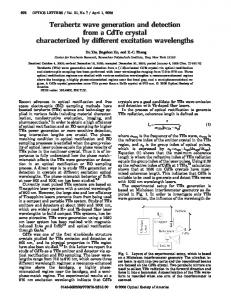
Fig. 6. The spectra of the emission from InGaAs HEMT. The arrows mark the maxima position for emission at 0.42 THz, 0.56 THz, and 1.0 THz obtained for UDS of 0.3 V, 0.6 V, and 0.8 V, correspondingly.
Fig. 7. The intensity of the resonant emission signal (left axis) versus drain-to-source voltage. Inverse resonant frequency (1/f ) versus drain voltage (right axis).
A few measured spectra are shown in Fig. 6. The spectra exhibit one main emission line. The peak emission frequency increases from ≈ 0.42 THz up to ≈ 1 THz with increasing UDS from 0.2 V to 0.8 V. No emission was observed until the drain current reached a certain threshold value of about 4.5 mA. Above the threshold, a strong emission signal (sharply increasing with the bias) was observed. The threshold behaviour can be clearly seen in Fig. 7 showing the resonant line emission intensity versus drain voltage. It should be underlined that in all cases of many InGaAs/AlInAs transistors on which we observed the emission signal, the emission signal appeared only when the transistor was driven into the saturation. The resonant frequency of the emission is determined by the sheet electron density under the gate, by the electron drift velocity, and the effective gate
90
W. Knap et al.
length LEFF . The latter depends on the geometry of the device but, in the saturation regime, is also affected by the drain voltage due to the gate length modulation effect. The effective gate length at zero drain LEFF = L + 2d, where L is the geometric gate length, d is the thickness of the wide band barrier layer (for our device d = 17 nm and LEFF = 94 nm). Let us now consider the dependence of the emission peak on the bias voltages. As the drain bias increases, the gate length modulation effect decreases the effective channel length [17]. The gate modulation occurs since in the saturation region the channel splits into two parts — an effective FET section, where gradual channel approximation still holds and a high field region, which is formed at the drain side of the channel and spreads toward the source with an increase in the applied source–drain voltage. The decrease in the effective length of the channel can be described by the phenomenological formula UDS − USAT , (2) ED where USAT is the drain-to-source saturation voltage and ED is the effective electric field. As a consequence, we expect that 1/f is a linear function of UDS − USAT . Figure 7 shows that the inverse of the resonant frequency (1/f ) versus the source– drain voltage (UDS − USAT ) can indeed be approximated by a straight line as predicted by this simple model. We determined the effective electric field in the high field region to be ED = 4 × 10⁴ V/cm, the saturation voltage was taken USAT = 240 mV — the voltage for which the first well-resolved resonant emission (f = 0.42 THz) was observed. LEFF (UDS ) = LEFF (0) −
5. Conclusions In conclusion, detection and emission of the THz radiation by plasma instability in field effect transistors was observed. The transistors used were based on different semiconductor structures (InGaAs/AlInAs, GaAs/GaAlAs, Si) that show a universality of the observed plasma instability. The experiments indicate that FETs are promising devices for resonant voltage tuneable detector operation. What is more, measurement on Si MOSFET show the possibility of using such detectors at room temperature. References [1] E.B. Cole, R. Woodward, D.A. Crawley, V.P. Wallace, D. Arnone, Proc. SPIE Int. Soc. Opt. Eng. 4276, 1 (2001). [2] B.H. Deng, C.W. Domier, A.J. Donne, K.C. Lee, N.C. Luhmann Jr., E. Mazzucato, T. Munsat, H. Park, M. van-de-Pol, IEEE MTT-S International Microwave Symposium Digest 3, 1587 (2002).
Terahertz Generation and Detection by Plasma Waves . . .
91
[3] N. Sekine, K. Hirakawa, M. Vosseburger, P.H. Bolivar, H. Kurz, Phys. Rev. B 64, 201323 (2001); R. Bratschitsch, R. Kersting, T. Muller, G. Strasser, K. Unterrainer, W. Fischler, R.A. Hopfel, Physica B 272, 375 (1999). [4] J.N. Heyman, P. Neocleous, D. Hebert, P.A. Crowell, T. Muller, K. Unterrainer, Phys. Rev. B 64, 085202 (2001); D. Hashimshony, A. Zigler, K. Papadopoulos, Phys. Rev. Lett. 86, 2806 (2001); T. Dekorsy, H. Auer, H.J. Bakker, H.G. Roskos, H. Kurz, Phys. Rev. B 53, 4005 (1996). [5] I. Iguchi, Supercond. Sci. Technol. 13, 93 (2000). [6] S. Hoffmann, M. Hofmann, E. Brundermann, M. Havenith, M. Matus, J.V. Moloney, A.S. Moskalenko, M. Kira, S.W. Koch, S. Saito, K. Sakai, Appl. Phys. Lett. 84, 3585 (2004). [7] A.A. Andronov, V.A. Kozlov, S.A. Pavlov, S.G. Pavlov, Sov. Techn. Phys. Lett. 14, 891 (1988). [8] R. Kohler, A. Tredicucci, C. Mauro, F. Beltram, H.E. Beere, E.H. Linfield, A.G. Davies, D.A. Ritchie, Appl. Phys. Lett. 84, 1266 (2004). [9] M. Dyakonov, M.S. Shur, Phys. Rev. Lett. 71, 2465 (1993); M. Dyakonov, M.S. Shur, in: Terahertz Sources and Systems, Ed. R.E. Miles, Kluwer Academic Publishers, Netherlands 2001, p. 187. [10] W. Knap, Y. Deng, S. Rumyantsev, J.-Q. L¨ u, M.S. Shur, C.A. Salor, L.C. Brunel, Appl. Phys. Lett. 80, 3433 (2002); W. Knap, Y. Deng, S. Rumyantsev, M.S. Shur, Appl. Phys. Lett. 81, 4637 (2002). [11] X.G. Peralta, S.J. Allen, M.C. Wanke, N.E. Harff, J.A. Simmons, M.P. Lilly, J.L. Reno, P.J. Burke, J.P. Eisenstein, Appl. Phys. Lett. 81, 1627 (2002). [12] W. Knap, J. L Ã usakowski, T. Parenty, S. Bollaert, A. Cappy, V.V. Popov, M.S. Shur, Appl. Phys. Lett. 84, 2331 (2004). [13] W. Knap, F. Teppe, Y.M. Meziani, N. Dyakonova, J. L Ã usakowski, F. Boeuf, T. Skotnicki, D. Maude, S. Rumyantsev, M.S. Shur, Appl. Phys. Lett. 85, 675 (2004). [14] W. Knap, J. L Ã usakowski, K. Karpierz, B. Orsal, J.L. Robert, J. Appl. Phys. 72, 680 (1992); G.E. Stillman, C.M. Wolfe, J.O. Dimmock, Solid State Commun. 7, 5 (1969). [15] W. Knap, V. Kachorovskii, Y. Deng, S. Rumyantsev, J.Q. Lu, R. Gaska, M.S. Shur, G. Simin, X. Hu, M. Asif-Khan, C.A. Saylor, L.C. Brunel, J. Appl. Phys. 91, 9346 (2002). [16] W. Knap, D. Dur, A. Raymond, C. Meny, J. Leotin, S. Huant, B. Etienne, Rev. Sci. Instrum. 63, 3293 (1992). [17] K. Lee, M.S. Shur, T.A. Fjeldly, T. Ytterdal, Semiconductor Device Modeling for VLSI, Prentice Hall, Englewood Cliffs, NJ 1993, p. 340.