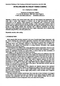
The MVIP-2 Architecture for H.263 Video Coding Matías J. Garrido, César Sanz, Marcos Jiménez, Juan M. Meneses Universidad Politécnica de Madrid. Spain {matias, cesar, mdavia}@sec.upm.es,
[email protected]
Abstract∗ MVIP-2, a flexible and efficient architecture that implements the core of a video coder according to Rec. H.263, is presented in this paper. It consists of a RISC that controls the scheduling of a set of specialized processors for the transforms (DCT and IDCT), quantizers (DQ and IQ), motion estimation (ME) and motion compensation (MC). The architecture also includes preprocessing modules for the input video signal from the camera and interfaces for external video memory and H.263 bit-stream generation. The architecture has been written in synthesizable Verilog and tested using standard video sequences. We are now prototyping MVIP-2 on a commercial development system based on an EP20K400BC652 FPGA and an ARM7TDMI RISC.
image each 75 seconds, considering 32Kbits/sec for transmission and reception. The image compression techniques can drastically reduce the bit-rate needed to encode the digital video signals. The compression techniques used take advantage of the peculiarities of the human vision system to reach compression ratios up to 100:1 [4]. Although a large quantity of useful techniques has been reported, nearly all the applications use the hybrid encoding scheme shown in Fig. 1, which is based on the reduction of the spatial and temporal redundancies existing in any natural sequence of images. Regulator
Frame Memory
+
DCT
Q
VLC
-
1. Introduction In the last 10 years, the evolution of digital technologies, together with the establishment of a set of standards widely followed by the industry, such as MPEG-2[1], MPEG-4[2] and H.263[3], has allowed the development of a wide range of applications: digital TV, HDTV, VoD, videotelephony, videoconferencing, etc. The applications implemented over low rate channels, as videotelephony, use low resolution formats such as CIF (Common Intermediate Format. Spatial resolution of 360 × 288 pels and temporal resolution of 30 frames/sec). Even so, usually the available bandwidth is roughly lower than that needed for working with a minimum level of performance. For example, a videophone using CIF with an ISDN (Integrated Services Digital Network) channel would allow the visualization of just one ∗
This work is being supported by grant TIC99-0927 from the Comisión Interministerial de Ciencia y Tecnología (CICYT) of the Spanish Government.
Preproc.
IQ
Buffer
Output
Inter/Intra IDCT
Input 0
+
Motion Compensation
+
Rec. Frame Memory
Motion Estimation
Fig. 1. Hybrid encoder for video compression.
The hybrid encoder reduces the temporal redundancy encoding the difference between each image and its prediction computed on the basis of previous or future images in the sequence. A transformation to the spatial frequency domain is applied to this difference and finally, the transformed coefficients are quantized. The spatial redundancy reduction is obtained by means of a coarse quantization of the higher spatial frequencies and Variable Length Coding (VLC). As the human vision system is less
sensitive to these higher spatial frequencies, the image quality remains acceptable while the output bit-rate is greatly reduced. In 1998, the ITU established the H.263 Recommendation that uses a number of encoding techniques tested in other standards such as MPEG-1 and MPEG-2 as well as more advanced ones. This paper details a very efficient and flexible architecture that implements a basic line H.263 video encoder, based on the hybrid encoding loop set out in Fig. 1. In section 2, the results of a survey of some of the architectures that implement H.263 encoders reported in the last 4 years are shown. In section 3 the MVIP-2 architecture is presented paying special attention to the operation scheduling. In section 4 the methodology followed in the development of the design is explained. In section 5 the obtained results and the tests carried out are shown. Finally, section 6 is devoted to the conclusions.
2. A survey of H.263 video encoding architectures The implementations that has been presented in international publications during the last 4 years can be classified into three groups: The first group contains the implementations based on general purpose microprocessors, including PCs or workstations. All the efforts are focused on the optimisation of the code that implements the encoder loop for the target microprocessor. A very representative proposal of this group is presented in [5], where the basic H.263 encoding loop is optimised for three different platforms: a 167 MHz Sun UltraSPARC-1 workstation, a 233 MHz Pentium II PC and a 600 MHz Pentium III PC, reaching a minimum of 10, 13 and 35 frames/sec for QCIF in tests with standard sequences. The second group contains architectures based on special microprocessors such as DSPs, vector parallel processors or multiprocessors. As more significant proposals, in [6] a multiprocessor architecture made up of interconnected nodes is presented; each node contains a RISC core adapted for video encoding, DRAM memory, a video interface and an external host interface. Using two nodes working at 120 MHz the system encodes 25 CIF images per second. In [7] a vector parallel processor is used, with a scalar core at 200 MHz, which encodes 21 frames/sec in QCIF. The third group includes the architectures based on a controller together with a set of specialised processors for the specific tasks of the encoding loop. In [8] an architecture based on a sequencer that implements the scheduling for a group of specialised processors, encoding and decoding simultaneously 30 CIF frames/sec is proposed. The system clock frequency is 54 MHz and the circuit has nearly 9
million gates. In [9] another architecture based on a dedicated sequencer and specialised processors is presented. It is implemented on a 80,000 gate Xilinx FPGA running at 30 MHz and carries out the basic line of H.263 with CIF and 30 frames/sec but without motion estimation. The architectures detailed lack flexibility because of their dedicated controller. Instead, the following ones use a programmable controller. In [10], an ARM RISC core at 200 MHz is used to carry out the transforms (DCT, IDCT) and quantizers (DQ, IQ) and controls a set of processors for motion estimation and compensation, video signal processing and external dynamic memory interfacing. The processors are implemented with about 40,000 gates and work at 66 MHz clock frequency. This system implements the encoder and decoder for the H.263 with QCIF and 29 frames/sec. In [11] an architecture based on a programmable address generator and a pipeline controller for a set of processors: the camera interface, the image filter, the loop DCT-DQ-IQ-IDCT, the motion estimation and the VLC is presented. With 80,000 gates and 27 MHz system clock, this architecture encodes QCIF at 30 frames/sec.
3. The MVIP-2 architecture MVIP-2 is an evolution from the MViP [12] to implement H.263 video encoding. In Fig. 2 the block diagram of MVIP-2 is shown. It consists of three functional blocks: CPU system, processing system and interface system. Furthermore, there are some external modules: a digital camera, flash and RAM memories to store code and data for the CPU and SDRAM for the video memory. CAMERA
VIDEO MEMORY
Flash RAM
CPU SYSTEM CPU SUBSYSTEM
RISC ARM7TDMI processor Decoder PIC
IMEM IVIDEOH IFRMEM IFRMEM
DQ IQ IDCT ME MC
IT
IT
IVIDEOV
IFRECMEM
PROCESSORS
DCT
MVIP-2
INTERFACE SYSTEM
INTERNAL MEMORIES
C R O S S B A R
M10 M13 M20 M24
M30 M40
M33 M41
M50 M51
PROCESSING SYSTEM
Fig. 2. Block diagram of MVIP-2.
The CPU system is made up of a RISC processor (ARM7TDMI), an address decoder and an interrupt controller (PIC). At boot time, the CPU runs a loader from flash which copies the application code and data to the RAM for a faster execution using this memory. The PIC supports 11 non-vectorized interrupts; the priority and the identification of the interrupting devices are software implemented. The processing system consists of specialised processors for implementing the direct and inverse cosine transform (DCT & IDCT), the direct and inverse quantization (DQ & IQ) and the motion estimation and compensation (ME & MC). The inter/intra decision is implemented by the ME and the RISC core, which also carries out the VLC. The processors can access internal memories (M10...M13, M20...M24, M30...M33, M40...M41, M50 and M51) through an interconnection network (CROSSBAR). The interface system is made up of a set of modules: for the camera (IVIDEOH, IVIDEOV), for the frame memory (IFRMEM), for the reconstruction memory (IFRECMEM), for the video memory (IMEM) and for the H.263 bit-stream generation (IT). The camera interface synchronizes input data with the MVIP-2 internal clock, selects one of two image fields if necessary and carries out a pre-processing that includes a separated bidimensional filtering in both horizontal (IVIDEOH) and vertical (IVIDEOV) components. The block IMEM manages the SDRAM refreshing and offers channels (using a request/acknowledge protocol) to the processors and interfaces for accessing the SDRAM. The processors and interfaces access to the channels can be simultaneous and IMEM manages the priorities in cases of conflict. The frame memory interface reads the filtered frames and stores them in the internal memory. The reconstruction memory interface reconstructs the frames and stores them in the video memory. Finally, the bit-stream interface (IT) assembles the output bit-stream with data elaborated by the RISC core. MVIP-2 works with three levels of pipeline: image-level, macroblock-level and pel-level. The interfaces IVIDEOH, IVIDEOV, IFRMEM and IFRECMEM work with an image-level-pipeline. IMEM supports frame-size logic pages and the processors use these pages to interchange the images. Each processor reads an image from a logic page, process it and stores the results on a different page for the next processor. A typical coding sequence is shown in Fig. 3: inside each frame period IVIDEOH reads an image from the camera and carries out the horizontal filtering, IVIDEOV carries out the vertical filtering, IFRMEM reads the filtered image and stores it, on a macroblock basis, in the internal memory (M10...M13) and, at the end of the coding loop,
IFRECMEM reads the IDCT output coefficients from M23 and M24 and stores them on a page of video memory. Table 1 shows the access sequence to the video memory logic pages corresponding to the coding sequence shown in Fig. 3. In the frame periods (T0...T5) the processors interchange images using seven logic pages (P0...P6), e.g. at T1 IVIDEOH writes the second frame (WR F2) using P1 while IVIDEOV reads the first frame (RD F1), now filtered in the horizontal dimension, from P0. After an initial latency all processors work in parallel using seven logic pages in video memory. IFRMEM, ME, MC, DCT, DQ, IQ, IDCT and IFRECMEM work with a macroblock level pipeline. Each processor reads a macroblock from one of the internal memories through the CROSSBAR, processes it and then writes the results in other internal memory (IFRMEM reads from video memory and IFRECMEM writes to video memory). Fig. 3 shows that after an initial latency, all processors work in parallel. Frame period
IVIDEOH, frame 1
IVIDEOH, frame 2
IVIDEOV, frame 1
IVIDEOH, frame3
IVIDEOH, frame4
IVIDEOV, frame 2
IVIDEOV, frame 3 Loop , frame 2
Loop , frame 1
ifrmem me mc dct dq iq/lrl idct ifrecmem Macroblock period
Initial latency
Fig. 3. Example of encoding sequence.
P0 P1 P2 P3 P4 P5 P6
T0
T1
T2
T3
T4
T5
IVIDEOH WR F1
IVIDEOV RD F1 IVIDEOH WR F2 IVIDEOV WR F1
IVIDEOH WR F3 IVIDEOV RD F2 IFRMEM RD F1
IVIDEOV RD F3 IVIDEOH WRF4 IVIDEOV
IVIDEOV RD F5 IVIDEOH WRF6 IVIDEOV
WR F3
IVIDEOH WR F5 IVIDEOV RDF4 IFRMEM RD F3
IVIDEOV WR F2
IFRMEM RD F2
IVIDEOV WR F4
IFRMEM
IFRECMEM
P-ME RD F2
IFRECMEM
P-ME RD F4
IFRECMEM
P-ME RD F3
IFRECMEM WR F4
P-ME WR F2
P-ME WR F3
P-ME WR F4
P-MC RD F2
P-MC RD F3
P-MC RD F4
IFRECMEM RD F2
IFRECMEM RD F3
IFRECMEM RD F4
WR F1
WR F5 RD F4
WR F3 WR F2
Table 1. Access to video memory pages sequence
Table 2 shows a typical inter coding sequence, where T0...T8 represent macroblock periods. The macroblocks to be processed (CF macroblocks) are stored alternatively in M10...M13 by IFRMEM (Ifrmem WR CF#). The Motion Estimator, which is based on EST3P [13] and EST3P-PAR [14] and implements a hierarchical Three-Step-Search algorithm, reads the CF macroblocks
(p-me 3×RD CF#) three times in order to make the prediction and once more to get the 1/2 pel accuracy. Finally, the Motion Compensator reads it once again on order to compute the difference with the prediction and to write the result alternatively in M20 and M21 (p-me WR CF#-REC#). The DCT processor reads these data (p-dct RD#) and stores the transformed coefficients in M30...M33 (p-dct WR#), from where they are read and quantized by DQ, which writes them in M40 or M41 (p-dq WR#). The IQ processor reads the quantized coefficients and calculates the inverse quantization and last, run, level (LRL) coding simultaneously; the dequantized coefficients are stored in M30...M33 (p-iq WR#) and the LRL coded coefficients in M50 or M51 (p-lrl WR#). The IDCT processor reads the dequantized coefficients and writes the spatial domain transformed pels in M23 or M24 (p-idct WR#), from where they are read by IFRECMEM (i-frecmem RD#). The LRL coefficients are read by IT ( i-tr RD#).
M 10 M 11 M 12 M 13 M 20 M 21 M 30 M 31 M 32 M 33 M 40 M 41 M 50 M 51 M 23 M 24
T0
T1
I-frmem WR CF0
p-me 3x RD CF0 Ifrmem WR CF1
T2
T3
T4
T5
T6
T7
T8
p-me p-mc I-frmem p-me p-me p-mc I-frmem WR 3x RD RD CF4 RD CF 4 WR CF8 RD RD CF4 CF4 CF0 CF0 p-me p-me p-mc I-frmem p-me p-me p-mc 3x RD RD CF1 RD CF WR 3x RD RD CF5 RD CF 5 CF1 1 CF5 CF5 I-frmem p-me p-me p-mc I-frmem p-me WR 3x RD RD CF2 RD CF2 WR CF6 3x RD CF2 CF2 CF6
p-me RD CF6
I-frmem p-me p-me p-mc WR RD CF2 RD CF3 RD CF3 CF3 p-mc p-dct p-mc p-dct WR RD 0 WR RD 2 CF0CF2REC0 REC2 p-mc p-dct p-mc WR RD 1 WR CF1CF3REC1 REC3 p-dct p-dq p-iq WR 0 RD 0 WR 0
p-me 3x RD CF7 p-dct RD 4
p-dct WR 1
p-dq WR 0
I-frmem WR CF7 p-mc WR CF4REC4 p-dct RD 3
p-idct RD 0
p-mc WR CF5REC5 p-dct WR 4
p-dq RD 1
p-iq WR 1
p-idct RD 1
p-dct WR 2
p-dq RD 2
p-iq WR 2
p-dct WR 3
p-dq RD 3
p-iq RD 0
p-dq WR 2
p-iq RD 2
p-dq WR 1
p-iq RD 1
p-dq WR 3
p-lrl WR 0
i-tr RD 0
p-lrl WR 2
p-lrl WR 1
i-tr RD 1
p-idct WR 0
I-frecmem
are 9 bits wide, M30...M33 are 12 bits wide, M40...M41 are 11 bits wide and M50...M51 are 15 bits wide. At image and macroblock level, the scheduling can be completely controlled by the RISC processor by means of the system interrupt or by polling: all the processors have a configuration register with a start bit and a status register with a done bit connected to the interrupt controller, the processors remain idle until the microprocessor sets their start bit and when the image or macroblock is processed they set its done bit which can generate an interrupt or can be polled. Moreover, the RISC core takes part in the VLC coding, the inter/intra decision as well as in the generation of the H.263 bit-stream. All the MVIP-2 processors work with a classic pel-level-pipeline. The controllers of the processors have been designed to modify the number of pipeline stages easily.
4. Design methodology The design methodology used has been oriented towards two objectives: 1) making the design flexible enough to evolve or be reused to implement the encoding loop for other standards and 2) dealing with the test of such a complex system in an efficient way. The flexibility is obtained through the use of an HDL for describing the design and using parameters when possible, e.g., the width of buses or the number of pipeline levels. These features will allow the design as a starting point to implementing an IP for the hybrid coding loop in which the encoders used nowadays are based.
SW RISC
MVIP-2 SPECIFICATION
RTL
VERILOG TESTBENCH
N
OK?
OK?
Y
N
OK?
Y
N
Y
GOLDEN RTL CONSTRAINS
TARGET LIBRARY
SYNTHESYZER
NETLIST
RD 0 p-idct WR 1
Table 2. Scheduling of the operations at macroblock level
LIBRARY
FORMAL VERIFICATION
OK?
N
Y
Although all the internal memories can store one macroblock, there are five groups with different data bus widths: M10...M13 are 8 bits wide, M20...M24
PROTOTYPING
Fig. 4. Simplified flow diagram of the design cycle.
An efficient verification is made by designing exhaustive functional testbenches with auto-test capabilities before the logic synthesis stage, and using formal verification techniques in the postsynthesis stage. The design cycle, represented in Fig. 4 using a simplified diagram, consists of four main stages. The first stage is the development of the software for the RISC processor and the Verilog RTL description of the hardware. A testbench that includes Verilog simulation models for the camera, the memories and the RISC allows the functional tests with HW/SW Verilog co-simulations to be carried out. In the second stage the design is synthesized using the Design Compiler from Synopsys and a netlist is obtained from the RTL description and the area and time restrictions. The third stage consists of the formal verification of the synthesized netlist using Formality (also from Synopsys) in order to validate the netlist against the RTL description. In the fourth stage, the design is synthesized with the and prototyped into the HSDT200 development system [15] based on an ARM7TDMI RISC and a 400 Kgate EP20K400BC652 FPGA from Altera. In Fig. 5, a block diagram of the testbench used in the prototyping stage is shown. The blocks inside the dashed line box represent the development system. The input frames are generated in real time by an I/O PCI board plugged into a PC. A logic analyzer allows the debugging of all the interfaces. RAM flash
multiICE
JTAG
RISC
logic analyzer SDRAM
Input frames PC
5V
a)
b)
Fig. 6. Original (a) and reconstructed (b) images of Miss America sequence image
pquant
PSNR Y (dB)
# bytes
#1 #2 #3 #4 #5 #6 #7 #8 #9 #10
16 12 12 12 12 12 12 12 12 12
36.01 36.27 36.17 36.25 36.09 36.10 36.20 36.24 36.38 36.29
1008 152 144 155 158 159 151 102 96 85
Table 3. System performance for the first 10 images of Miss America sequence
Output H.263 stream
FPGA
shows the number of bytes per image in the H.263 stream and the Peak Signal to Noise Ratio (PSNR) per image for the first 10 images of the sequence.
3.3V
In the second stage, we have carried out a logic synthesis with Design Compiler using a target library from Altera. A formal verification of the synthesized modules has been made in the third stage. Finally, in the fourth stage, the design has been synthesized with FPGA Compiler II. In Fig. 7, the gate size for all processors and interfaces is shown1. Kgates 100
Fig. 5. Block diagram of the prototype testbench.
90 80
5. Results
70
In the first stage of the design cycle an RTL description of MVIP-2 and a first version of the software for the ARM processor have been obtained. Exhaustive functional tests with fixed and random data sequences have been carried out. The encoder has also been tested using QCIF standard sequences such as Foreman, Silent or Miss America and the H.263 stream has been tested using ClipPlayer [16]. As an example, the first (intra with quantization step of 16) and seventh (inter with quantization step of 12) frames of Miss America together with their reconstructed versions are shown in Fig. 6. Table 3
60 50 40 30 20 10 0 IVH
IVV
IFR
IFREC IMEM XBAR
DQ
IQ
DCT
IDCT
ME
MC
Fig. 7. Size of processors and interfaces (Kgates).
1
This data does not include the filters inside the IVIDEO_H (IVH) and IVIDEO_V (IVV) processors.
Fig. 8 shows the use of the FPGA internal memory. An MVIP-2 version with a DCT processor to carry out both DCT and IDCT and with entire-pel accuracy for motion estimation has been fitted into the FPGA using 98% of the logic cells and 52% of the internal memory resources. The tests carried out in the prototype have shown that the system is capable of working up to 24 MHz system clock and can encode QCIF at 60 fps, equivalent to CIF at 15 fps.
References [1]
[2] [3] [4] [5]
Kbits 100 90 80 70 60
[6]
50 40 30 20
[7]
10 0 M10...M51
DCT
IDCT
ME
Fig. 8. Internal memory used by MVIP-2.
[8]
6. Conclusions In this paper a flexible and efficient architecture that implements a basic line H.263 encoder is presented. The design methodology has been oriented to providing a reusable design, to ease an exhaustive testing and to fast-prototyping; features that will allow its transformation in an IP. A Verilog RTL description, whose functionality and synthesizability has been exhaustively tested, has been obtained. MVIP-2 can encode QCIF sequences at 60 frames/sec with a 24 MHz system clock, or CIF sequences at 15 fps, which is better than other implementations with a similar degree of flexibility (see Table 4 for a comparison of our proposal and the proposals summarized in section 2). Ref
fps/Size
CLK (MHz)
Kgates
[5] [6] [7] [8]
35/QCIF 25/CIF 21/QCIF 30/CIF
600 120 200 54
9000
[9]
30/CIF
30