VOLUME 86, NUMBER 11
PHYSICAL REVIEW LETTERS
12 MARCH 2001
Unambiguous Interpretation of Atomically Resolved Force Microscopy Images of an Insulator A. S. Foster,1, * C. Barth,2 A. L. Shluger,1 and M. Reichling2 1
Department of Physics and Astronomy, University College London, Gower Street, London WC1E 6BT, United Kingdom 2 Department Chemie, Universität München, Butenandtstraße 5-13, 81377 München, Germany (Received 4 October 2000) The (111) surface of CaF2 was imaged with dynamic mode scanning force microscopy and modeled using atomistic simulation. Both experiment and theory showed a clear triangular contrast pattern in images, and theory demonstrated that the contrast pattern is due to the interaction of a positive electrostatic potential tip with fluorine ions in the two topmost surface layers. We find a good agreement of position and relative height of scan line features between theory and experiment and thus establish for the first time an unambiguous identification of sublattices of an insulator imaged by force microscopy. DOI: 10.1103/PhysRevLett.86.2373
Recently, there has been considerable progress in atomic resolution imaging of insulator and semiconducting surfaces using dynamic mode scanning force microscopy (SFM) [1,2]. However, the identity of atomic size features seen in these images in most cases was impossible to establish. The long-standing problem of reliable interpretation of SFM images hampers further application of SFM to quantitative studies of reactivity, adsorption, chemical reactions, tip-induced manipulation, and other surface processes on the atomic scale. It is most acute for highly symmetric surfaces, such as alkali halides [3], where uncertainty in the tip atomic structure prevents one from distinguishing anion and cation sublattices. However, more reliable interpretation should be possible for less symmetric surfaces, such as fluorides. In this Letter, theoretical analysis of particular features in highly resolved SFM images of a CaF2 (111) surface using atomistic modeling provided the first unambiguous interpretation of SFM image features on an insulating binary system. Reliable imaging of the subtle features in the SFM contrast patterns that is required for this kind of analysis has been made possible by the sophistication of the experimental apparatus and techniques, as described below. The results reported here are taken from three different series of measurements on freshly cleaved surfaces with two different tips, all yielding very similar results reproducible under the applied tip preparation methods. Experiments were performed with a scanning force microscope (Omicron STM/AFM) operated in the dynamic mode and in an ultrahigh vacuum (UHV) system with a base pressure in the low 10210 mbar range. Dynamic mode force microscopy measured the change in frequency of an oscillating cantilever due to the interaction of a tip at the end of the cantilever with the surface. P-doped 共1.5 V cm21 兲 silicon cantilevers (Nanosensors) with a spring constant of 6 N兾m were excited to vibration at their resonance frequency of 77 kHz with an amplitude stabilized to 35 nm. More details on our SFM system can be found in Ref. [4]. It is now equipped with a new digital demodulator (Nanosurf) providing utmost stability and a signal-to-noise ratio improved by a factor of 10 compared 0031-9007兾01兾86(11)兾2373(4)$15.00
PACS numbers: 68.35.Bs, 02.70.Ns, 68.37.Ps
to previous measurements. Another major experimental difference to previous studies is that, for the present work, we operated the system at an extremely small loop gain for the distance control loop and, thus, effectively used a constant height mode rather than a constant frequency shift mode. Since there is no direct measure of tip-surface separation in the experiment, constant height in this context refers to the fact that the average position of the base of the cantilever is not changed due to interaction with the surface. Cantilever resonance frequency detuning reflects the tip-surface interaction. The average detuning across a whole image is used as a relative measure of distance in constant height mode, since the mean tip-surface separation is determined by the background forces, i.e., the forces not affecting atomic contrast, such as macroscopic van der Waals and electrostatic forces. Tips used in this study were not sputtered and therefore coated by oxide, hydroxide, and possibly other molecules of unknown composition. Furthermore, we found that it is most favorable for atomic resolution imaging on fluorides to bring the tip in slight contact with the surface prior to taking images in the dynamic mode. This method of tip preparation was also performed prior to the experiment reported here, and it is likely that the tip has picked up surface constituents during this procedure. The sample was taken from commercial single crystals of highest available quality CaF2 (Korth, UV grade crystals). Surfaces were prepared by cleavage along the (111) surface in UHV. For measurements, an area with a small density of macroscopic steps was selected. To minimize electrostatic forces due to residual surface charging, a tip bias voltage of 3.3 V was applied during the experiment. The theoretical model used in this study is the same as that described in Refs. [5,6]. A schematic diagram of the tip and surface setup used in the calculations is shown in Fig. 1. The model tip is composed of a conducting cone with an oxide nanotip at the spherical apex of the cone. For this purpose, we use a 64-atom MgO cube embedded into the macroscopic tip. This has been shown previously [7] to well represent the potential of oxidized or contaminated silicon tips and ionic clusters. The local © 2001 The American Physical Society
2373
VOLUME 86, NUMBER 11
PHYSICAL REVIEW LETTERS
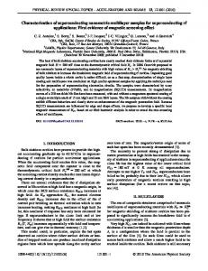
FIG. 1. Schematic of the model setup. U is the bias between conducting tip (radius R) and conducting substrate. The first layer of the fluorine terminated CaF2 (111) surface is shown atomistically. The calcium layer is labeled 1, the outermost fluorine layer is labeled 2, and the lower fluorine layer is labeled 3. The layers are separated by about 0.08 nm.
potential from the apex of the tip has atomic dimensions [7] and probes only a small area of the surface. To model a positive or negative potential tip, the cube is orientated so that it is symmetric about the z axis with either a single magnesium or oxygen ion at the corner pointing to the surface. Note that the pattern of contrast and the resultant features discussed here depend on the sign of the potential from the tip and its gradient, which are not significantly dependent on the orientation of the nanotip [8]. The tip-surface interaction includes the following: (i) the microscopic chemical force between atoms in the tip and the surface, which includes the van der Waals force between ions; (ii) the macroscopic van der Waals force between the tip and the surface; and (iii) the electrostatic force due to work functions, charging, and polarization of conducting materials. The macroscopic and microscopic forces are integrated in the same way as in earlier studies [5]. For bulk CaF2 , the sample used in experiments is so thick (3– 5 mm) that the distance between the tip and the conducting substrate makes the image force [9] negligible. The distance dependence of the van der Waals force is calculated using a Hamaker constant of 1 eV [10]. The microscopic force is calculated using a periodic static atomistic simulation technique and the MARVIN2 code [11]. The empirical parameters used for the tip, CaF2 surface, and tip-surface interactions are the same as in Ref. [6]. They reproduce the elastic and dielectric properties of bulk CaF2 and give good agreement with periodic Density Functional Theory calculations of the surface structure. The unit cell used in the simulation is equivalent to extending the single layer shown in Fig. 1 three times in both the lateral and vertical directions. The bottom of the nanotip and the top of the CaF2 surface (top two 2374
12 MARCH 2001
layers) are relaxed explicitly with respect to microscopic forces in the system. The oscillations of the cantilever are simulated with the experimental parameters given above, using the method described in Ref. [5]. One can characterize the macroscopic properties of the tip necessary for interpretation of surface images by fitting the parameters of the model to reproduce the experimental frequency detuning vs distance curves [12,13]. In this study, a force curve was taken directly after a series of measurements analyzed here. It was then fitted with our theoretical model by varying tip radius, R, and applied bias voltage, U, which directly changes the background van der Waals and electrostatic forces, respectively. Details of the procedure are discussed in Ref. [14], while we here just note that the tip turned out to be rather blunt. This is in accordance with our experience from many measurements, that best atomic resolution is obtained with tips that are blunt on the macroscopic scale but have a stable cluster at their end. For these tips, the background force is dominated by the van der Waals interaction between the macroscopic tip and the surface, while long-range electrostatic interactions are compensated by applied bias voltage and are of minor importance. Such tips can sense the atomic size features with the terminating cluster atom but can also be well stabilized with respect to disturbances. Figure 2 shows an experimental image generated with an average frequency detuning of 2126 Hz. The remarkable feature of this, and other images obtained under similar conditions, is a triangular pattern with apexes along the [121] and equivalent directions. The origin of the contrast features can be seen more clearly in the example scan line, which demonstrates that the triangular nature of the contrast pattern in the image is due to a secondary smaller maximum, or shoulder, next to the largest maximum in the scan lines. These images are reproducible, and a detailed analysis of images taken in different conditions is given in Ref. [14]. For quantitative characterization, we made a statistical analysis of 73 pairs of primary and secondary maxima in 15 separate scan lines and determined the position of the secondary features and their height relative to the primary peaks. This gives the average distance of the secondary peak from the primary as 0.25 6 0.05 nm, and the ratio of the heights of the primary and secondary maxima as 0.51 6 0.37. It should be noted that problems related to thermal drift make it difficult to establish a reference height when calculating the ratio of peak heights, and this reduces the accuracy of this measurement. This problem has been addressed in a more extensive statistical analysis [14]. The apex of SFM tips can produce a positive or negative local electrostatic potential, dependent on structure and contamination. To model a tip with positive potential, we use a nanotip orientated so that a Mg21 ion was at the apex [7]. Figure 3 shows a simulated image taken at a tip-surface separation of 0.4 nm with this tip. The smallest tip-surface separation used in the theoretical study was chosen to match the average detuning seen in the
VOLUME 86, NUMBER 11
PHYSICAL REVIEW LETTERS
FIG. 2. Experimental SFM image 共3.0 3 2.2 nm2 兲 and scan line of the CaF2 surface taken at constant height with an average detuning of 2126 Hz. The white line is along the [121] direction and shows the position of the scan line.
experimental image in Fig. 2. Maximum detuning in the image is over the most protruding F2 ions in the surface, F(2). The strong attraction between the positive potential from the tip and the negative potential over the F2 ions dominates the interaction. The displacement of the F2 ions due to interaction with the tip also increases the contrast [5]. The F2 ions displace by about 0.02 nm towards the tip while scanning. The interaction with the deeper F2 ion, F(3), can also be seen clearly in the image. This causes the bright areas centered on the F(2) sites to appear triangular, with contrast decaying slowly when passing from a F(2) to a F(3) site, compared to passing from a F(2) to a Ca(1) site. Analysis of scan lines shows that a shoulder is located at 0.22 nm next to the main peak, with a height ratio of 0.27. In order to model a tip with a negative electrostatic potential due to an oxide layer or contamination by an anion, the next simulations were performed with the nanotip orientated so that an O22 ion was at the apex. Figure 4 shows a simulated image at a smallest tip-surface separation of 0.4 nm with this tip. Note that, although the tip now has an opposite potential, the average detuning in the image in Fig. 4 is the same as in Fig. 3. This reflects the fact that the average detuning is really a measure of average background force at a given distance, which is independent of the sign of the electrostatic potential from the tip.
12 MARCH 2001
FIG. 3. Simulated detuning image and scan line produced at a constant height (with reference to the Ca sublattice) of 0.4 nm over the CaF2 (111) surface with a positive potential nanotip. The average detuning for the image was 2126 Hz. The numbers on the schematic atoms refer to the labels in Fig. 1. The white line is along the [121] direction and shows the position of the scan line.
The strong attraction between the negative potential from the tip and the positive potential over the Ca21 ions dominates the interaction causing maximum detuning in the image over the Ca(1) sites. Surface relaxation also plays a role, with the Ca21 ions displacing towards the tip by about 0.01 nm during scanning. An increase in contrast can be seen halfway between bright spots along the direction parallel to the white line and along other equivalent directions. Calculated scan lines show a secondary maximum between the two F2 ions at 0.33 nm from the main peaks. This reflects the weaker repulsion over the deeper F(3) site compared to the protruding F(2) sites, making the maximum peaks, primary and secondary, asymmetric and translates directly into the simulated images as a slower decay of brightness on one side of Ca21 ions. However, the spots remain effectively “disklike,” as the secondary maximum is only 0.11 of the height of the primary maximum. Comparison of the experimental and theoretical images demonstrates good agreement in the case of a positive potential tip imaging fluorine as bright. The experimental image in Fig. 2 and the theoretical image in Fig. 3 both demonstrate a triangular contrast pattern, and scan lines 2375
VOLUME 86, NUMBER 11
PHYSICAL REVIEW LETTERS
12 MARCH 2001
of the bright spots giving the contrast a triangular pattern. Further support for these results was seen in a separate experiment where the contrast was seen to change directly from disklike to triangular in one image due to a tip change. In this Letter, we demonstrate that by combining sophisticated experiment and theory it is possible to obtain atomic resolution and unambiguous image interpretation for a binary insulator. These results give great hope for future work on other complex insulators. A prerequisite for success is the ability to reliably image and interpret the subtle features characterizing these complex systems. We believe that this is an important step forward to quantitative atomic scale chemical resolution on insulators. A. S. F. acknowledges support from EPSRC and thanks A. Rohl for help with the MARVIN2 code. We thank R. Bennewitz, W. Allers, F. Giessibl, and H. Hug for stimulating discussions. Financial support by NATO CRG 974075 is gratefully acknowledged.
FIG. 4. Simulated detuning image and scan line produced at a constant height (with reference to the Ca sublattice) of 0.4 nm over the CaF2 (111) surface with a negative potential nanotip. The average detuning is 2126 Hz. The numbers on the schematic atoms refer to the labels in Fig. 1. The white line is along the [121] direction and shows the position of the scan line.
from those images show a shoulder next to the main peak. There is also good agreement between the position and relative size of the shoulders in scan lines at similar frequency detuning: Theory predicts shoulders at 0.22 nm from the main peak with 0.27 height ratio, compared to an average position of 0.25 6 0.05 nm and height ratio of 0.51 6 0.37 from experiment. In contrast, the modeling with a negative potential tip predicts the second maximum at 0.33 nm from the main peak with a height ratio of 0.11, resulting in the disklike contrast pattern. Thus, the experimental results agree with only one of two theoretical models considered. Although other more complex tip models are possible, we believe that a quantitative agreement between calculated and statistically analyzed experimental scan lines proves that our model reproduces the fundamental tip sensing properties. These results demonstrate that the apex of the tip used in the experiment had a positive local electrostatic potential and that the protruding F(2) sites were seen as bright in the image, with the deeper F(3) sites producing an elongation
2376
*Current address: Laboratory of Physics, Helsinki University of Technology, FIN-02015, Helsinki, Finland. Electronic address:
[email protected] [1] Proceedings of the First International Workshop on Noncontact Atomic Force Microscopy, edited by S. Morita and M. Tsukada [Appl. Surf. Sci. 140, 1 (1999)]. [2] Proceedings of the Second International Workshop on Noncontact Atomic Force Microscopy, edited by R. Bennewitz, C. Gerber, and E. Meyer [Appl. Surf. Sci. 157, 1 (2000)]. [3] R. Bennewitz, A. S. Foster, L. N. Kantorovich, M. Bammerlin, C. Loppacher, S. Schär, M. Guggisberg, E. Meyer, and A. L. Shluger, Phys. Rev. B 62, 2074 (2000). [4] C. Barth and M. Reichling, Surf. Sci. Lett. 470, L99 (2000). [5] A. I. Livshits, A. L. Shluger, A. L. Rohl, and A. S. Foster, Phys. Rev. B 59, 2436 (1999). [6] A. S. Foster, A. L. Rohl, and A. L. Shluger, Appl. Phys. A (to be published). [7] P. V. Sushko, A. S. Foster, L. N. Kantorovich, and A. L. Shluger, Appl. Surf. Sci. 144 –145, 608 (1999). [8] A. I. Livshits, A. L. Shluger, and A. L. Rohl, Appl. Surf. Sci. 140, 327 (1999). [9] L. N. Kantorovich, A. S. Foster, A. L. Shluger, and A. M. Stoneham, Surf. Sci. 445, 283 (2000). [10] R. H. French, R. M. Cannon, L. K. DeNoyer, and Y. M. Chiang, Solid State Ion. 75, 13 (1995). [11] D. Gay and A. Rohl, J. Chem. Soc. Faraday Trans. 91, 925 (1995). [12] M. Guggisberg, M. Bammerlin, C. Loppacher, O. Pfeiffer, A. Abdurixit, V. Barwich, R. Bennewitz, A. Baratoff, E. Meyer, and H.-J. Güntherodt, Phys. Rev. B 61, 11 151 (2000). [13] A. S. Foster, L. N. Kantorovich, and A. L. Shluger, Appl. Phys. A (to be published). [14] C. Barth, A. S. Foster, M. Reichling, and A. L. Shluger, J. Phys. Condens. Matter 13, 2061 (2001).