Oct 24, 2008 - AbstractâThe origin of drain disturb in NOR Flash EEPROM cells under channel ... control and a unique recovery procedure for over-erased cells .... of this subsection, we furnish additional experimental data. (Figs. 4â 6) that ...
IEEE TRANSACTIONS ON ELECTRON DEVICES, VOL. 51, NO. 5, MAY 2004
701
Drain Disturb During CHISEL Programming of NOR Flash EEPROMs—Physical Mechanisms and Impact of Technological Parameters Deleep R. Nair, Student Member, IEEE, S. Mahapatra, Member, IEEE, S. Shukuri, and Jeff D. Bude, Associate Member, IEEE
Abstract—The origin of drain disturb in NOR Flash EEPROM cells under channel initiated secondary electron (CHISEL) programming operation is identified. A comparative study of drain disturb under channel hot electron (CHE) and CHISEL operation is performed as a function of drain bias and temperature on bitcells having different floating gate length and junction depth. The disturb mechanism is shown to originate from band-to-band tunneling under CHISEL operation, unlike that under CHE operation that originates from source–drain leakage. The effect of technological parameters (channel doping and drain junction depth) on CHISEL drain disturb is studied for both the charge gain (erased cell) and charge loss (programmed cell) disturb modes. Fullband Monte Carlo device simulations are used to explain the experimental results. It is shown that methods for improving CHISEL programming performance (higher channel doping and/or lower drain junction depth or halo) increase drain disturb, which has to be carefully considered for efficient design of scaled cells. Index Terms—Band-to-band tunneling, channel hot electron (CHE), channel-initiated secondary electron (CHISEL), device scaling, drain disturb, Flash EEPROMs, hot carriers, Monte Carlo simulation.
I. INTRODUCTION
C
HANNEL-INITIATED secondary electron (CHISEL) injection is an excellent programming mechanism for NOR Flash EEPROMs [1]–[5]. It relies on impact ionization feedback, is activated by the application of a negative substrate and provides high-energy electrons that get injected bias into the floating gate (FG) over a spatially broad area in the channel [1]–[9], as schematically shown in Fig. 1(a). Compared to channel hot electron (CHE) injection [10], CHISEL injection provides lower voltage and lower power operation and faster under for equivalent programming time equivalent programming power. CHISEL injection also offers self-convergent programming leading to excellent threshold control and a unique recovery procedure for voltage over-erased cells [1]–[5], [9], [11], [12] not available under conventional CHE programming [13]. Manuscript received October 15, 2003; revised January 22, 2004. The review of this paper was arranged by Editor M.-C. Chang. D. R. Nair and S. Mahapatra are with the Department of Electrical Engineering, Indian Institute of Technology, Bombay 400076, India (e-mail: drnair@ ee.iitb.ac.in). S. Shukuri is with Renesas Technologies, Tokyo, Japan. J. D. Bude is with Agere Systems, Allentown, PA 18101 USA. Digital Object Identifier 10.1109/TED.2004.825821
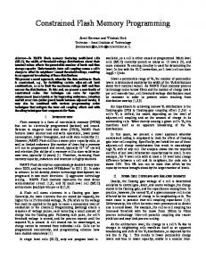
Fig. 1. (a) Schematic of CHISEL injection mechanism. Channel electrons, heated by lateral electric field create primary electron-hole pairs by impact ionization (M1). Primary holes flow to the substrate and in the presence of high transverse electric field (due to negative substrate bias) create secondary electron-hole pairs by impact ionization (M2). The secondary electrons move toward the interface and those having energy greater than 3.1 eV get injected into the FG [1]–[9] (b) Schematic of a NOR Flash array showing cells under (A) program and (B) drain disturb condition.
Drain disturb during programming is an important reliability issue for NOR Flash EEPROMs [2], [10]. It causes a threshold voltage shift in cells that have unselected word line (WL) but share the same bit line (BL) of a cell that is being programmed, as shown in Fig. 1(b). For a given drain bias , drain disturb might get aggravated during CHISEL programming due to the presence of negative that results across the drain junction. in higher transverse field Therefore it is necessary to systematically study drain disturb during CHISEL operation, identify its origin and quantify
0018-9383/04$20.00 © 2004 IEEE
Authorized licensed use limited to: INDIAN INSTITUTE OF TECHNOLOGY BOMBAY. Downloaded on October 24, 2008 at 00:34 from IEEE Xplore. Restrictions apply.
702
IEEE TRANSACTIONS ON ELECTRON DEVICES, VOL. 51, NO. 5, MAY 2004
TABLE I DEVICES USED IN THIS STUDY. V (V FOR I =V = 5 �A/0.8 V) (V FOR I = 1 �A, V = 0) MEASURED ON IDENTICAL AND V FG—CG SHORTED FETS
its dependence on programming biases and technological parameters, which to the best of our knowledge has not been done so far. The scope of this paper is twofold. First, the origin and physical mechanism of drain disturb under CHISEL operation is identified. This is done by measuring the differences in drain disturb behavior between CHISEL and CHE operation under varying bias and temperature and on bitcells having different and source/drain (S/D) junction structure. FG length It is clearly shown that CHISEL drain disturb originates from band-to-band tunneling. This is unlike CHE operation where drain disturb is known to originate from S/D leakage [17]. It has been suggested that high CHISEL programming is scaled by suitably efficiency can be maintained as adjusting the technological parameters that increases across the drain junction [5], [15], [16]. However increase in also increases drain disturb, which can adversely affect the program/disturb margin and therefore calls for careful attention. In the latter part of the paper, the impact of variation in technological parameters (channel doping and S/D junction scaling on CHISEL program and drain disturb depth) and performance is studied. The physical mechanism responsible for the observed drain disturb trends (as technological parameters are varied) is justified using full band Monte Carlo device simulations. Our results indicate that while trying to achieve is scaled, it is possible high programming efficiency as to keep drain disturb under control and therefore maintain the advantages of CHISEL programming. II. EXPERIMENTAL The devices used in this paper were fabricated using a state-of-the-art 0.18- m triple-well process featuring advanced modules such as shallow trench isolation and self-aligned S/D contacts leading to cell area of about 0.45 m . Measurements were performed on isolated, fully scaled bitcells having finished of 0.17 through 0.34 m, width (W) of 0.3 m, tunnel oxide and ONO interpoly dielectric (IPD) thickness of of about 12 and 20 nm, respectively, and gate coupling 0.55. Four different (D1, D2, D3, and D4) types of cells were fabricated to study the impact of technological parameters on CHISEL program and disturb performance. Their doping and junction breakdown schemes, junction depth, natural are mentioned in Table I. voltage Drain disturb measurements were performed at identical and as programming, but with zero control gate bias
to simulate an unselected WL. CHISEL and CHE programming V and V respectively (source were done at grounded). Uniform channel erase (source, drain and substrate V. was defined as to grounded) was done at A at V. The programmed and erased obtain V and V respectively. levels are defined as is defined as time for a change of 0.1 V Disturb time during disturb transients. Note, lower implies higher drain disturb and vice versa. Drain disturb phenomena is studied for both the charge gain (CG) (on erased cell) and charge loss (CL) (on programmed cell) disturb modes. Simulations were performed on FG-contacted devices (FG and control gate are shorted) having structure and doping profile identical to the measured bitcells. The structure and doping was obtained from a well-calibrated process simulation, whose output was used as the basis for device simulation. After obtaining the electrostatic potential distribution of the device from drift-diffusion solution, hot-carrier simulations were performed using a physics-based fullband Monte Carlo simulator (SMC) , substrate , and gate cur[9]. The simulated drain rents agree well with measurements. III. RESULTS AND DISCUSSION A. Program and Disturb Transients Fig. 2(a) shows CHE and CHISEL programming transients of 0.26- m cell. Measurements were done under idena s. tical bias and under equivalent programming time of Identical bias results in about five times faster CHISEL prois achieved by a 0.5 V increase in gramming speed. Identical (at identical ) for CHE operation. The relative comparison of CHE and CHISEL programming transients are similar for bitcells having different technological parameters and values and is consistent with previous reports [5]. Fig. 2(b) shows the CHE and CHISEL drain disturb transients corresponding to Fig. 2(a), measured under identical conditions. CHISEL operation always bias and equivalent shows both CG and CL disturb. CHE operation always shows CG disturb, while CL disturb is observed only under high (not considered in this paper). For the present 0.26- m cell, drain disturb is always higher for CHISEL operation irrespective of whether the comparison with CHE operation . However, is made under identical bias or under identical unlike the programming transients, the relative comparison of CHE and CHISEL disturb transients show a strong dependence values as shown in the on technological parameters and next subsection. B. Physical Mechanism of Drain Disturb Fig. 3 shows the dependence of CG under CHE and m cells having CHISEL operation, measured on two different S/D junction depths. For both CHE and CHISEL decreases and drain disturb increases with inoperation, crease in . However, CHE CG disturb increases with an increase in junction depth, while CHISEL CG disturb increases with a decrease in junction depth. This opposite trend indicates that the origin and physical mechanism of drain disturb is different under CHE and CHISEL operation.
Authorized licensed use limited to: INDIAN INSTITUTE OF TECHNOLOGY BOMBAY. Downloaded on October 24, 2008 at 00:34 from IEEE Xplore. Restrictions apply.
NAIR et al.: DRAIN DISTURB DURING CHISEL PROGRAMMING OF NOR FLASH EEPROMS
0
Fig. 2. (a) Programming transients of a L = 0:26 �m cell under CHE and CHISEL programming operation under identical bias and equivalent T conditions. V was defined as V required to have I = 5 �A at V = 0:8 V. (b) Drain disturb transients of a L = 0:26 �m cell for CHE and CHISEL operation under identical bias and equivalent T conditions. CHISEL shows lower disturb time (0.1 V change in V ) compared to a CHE operation.
0
Fig. 3. Disturb time as a function of drain bias of L = 0:26 �m cells having different S/D junction depth under CHE and CHISEL operation. Disturb time reduces for CHE but increases for CHISEL operation with reduction in junction depth.
CG disturb is due to electron injection into FG. The electron source could be either S/D leakage and/or band-to-band tunneling (BBT) near the drain junction. It is well known that CHE
703
drain disturb is caused by heating and subsequent injection of electrons originating from S/D leakage as the device is biased under subthreshold condition [17]. However during CHISEL is higher because programming (disturb) operation the cell induced body shift, which reduces S/D leakage. On the of in CHISEL operation results in other hand, the presence of across the drain junction and higher BBT. Therelarger fore, BBT generated electrons get heated by the junction field and get attracted toward FG by the positive FG charge (erased state) and cause CG disturb. CL disturb is caused either by electrons tunneling from FG to for drain or by hot hole injection into FG. However, similar both CG and CL under CHISEL operation implies equivalent carrier fluence into FG. We believe this is possible only when CL disturb is due to hole injection into FG and not due to elecon tron tunneling out of FG as there is a large difference in [see Fig. 2(b)]. Therefore, BBT generated the application of holes get heated by the junction field and get attracted toward FG by the negative FG charge (programmed state) and cause is used, BBT-induced CL disturb. Note that unless very high hole generation and its subsequent injection and, therefore, CL disturb is absent for CHE operation. The above model is consistent with the results shown in Fig. 3. S/D leakage, BBT, and carrier heating increase with an . Therefore, decreases with an increase in increase in for both CHE and CHISEL operation. Note, S/D leakage increases while BBT reduces with increase in S/D junction depth. Therefore, CG drain disturb for CHE operation increases while that for CHISEL operation decreases with increase in S/D junction depth, as shown in Fig. 3. In the remaining part of this subsection, we furnish additional experimental data (Figs. 4– 6) that validates the above drain disturb model. dependence of and during drain Fig. 4 shows the disturb measurements under CHE and CHISEL operation at a of 3.7 V. Similar dependence of the reciprocal of constant (i.e., drain disturb) and on ascribes their common decreases with decrease in for origin. It can be seen that CHE operation (CG), but remains almost constant for CHISEL operation (both CG and CL). This is expected since S/D leakage increases while BBT remains almost constant with the reduction . in Fig. 5 shows the temperature dependence of for a m cell measured at identical under CHE and decreases drastically with an CHISEL operation. CHE CG increase in temperature. This is expected due to the increase of S/D leakage with increase in temperature. On the other hand, drain disturb under CHISEL operation shows a weak increases slightly while CL temperature dependence. CG decreases slightly with an increase in temperature. Note at a higher temperature, carrier heating decreases slightly due to increased phonon scattering while BBT increases slightly due to a weak phonon-assisted mechanism [18]. These mutually competing but weak temperature dependent mechanisms result in weak but positive (for CL) and negative (for CG) temperature dependence of CHISEL drain disturb. and Fig. 6 shows the erase -level dependence of CG for m cells under CHE and CHISEL operation at . Once again, similar dependence of the reciprocal identical
Authorized licensed use limited to: INDIAN INSTITUTE OF TECHNOLOGY BOMBAY. Downloaded on October 24, 2008 at 00:34 from IEEE Xplore. Restrictions apply.
704
IEEE TRANSACTIONS ON ELECTRON DEVICES, VOL. 51, NO. 5, MAY 2004
Fig. 4. Disturb time and substrate current during disturb as a function of FG length for CHE and CHISEL operation under constant bias. Disturb time for CHE but remains almost constant for decreases with decrease in L CHISEL operation.
Fig. 6. Disturb time and substrate current as a function of initial threshold voltage of an erased cell of a L 0.26-�m cell under CHE and CHISEL operation. Disturb under CHE condition shows a strong sensitivity to the threshold voltage in contrast to CHISEL.
=
The above results (Figs. 3–6) clearly show that it is BBT and not the S/D leakage that leads to CHISEL drain disturb. Note that changes in technological parameters affect BBT in a much different way than S/D leakage, which is discussed in the following subsection. A similar study for CHE drain disturb is beyond the scope of the present paper. C. Effect of Technology Parameters on Drain Disturb (CHISEL)
=
Fig. 5. Disturb time as a function of inverse temperature of a L 0.26-�m cell for CHE and CHISEL operation under constant bias. Disturb time shows weak temperature dependence for CHISEL compared to CHE operation.
of and on erase level ascribes their common origin. It can be clearly seen that drain disturb for CHE operation is value, while that for quite sensitive to small changes in erase CHISEL operation shows almost an independent behavior. Note level determines the FG voltage of the cell. that erase , hence, strongly impacts S/D Small changes in erase leakage in the subthreshold regime for CHE operation, while BBT during CHISEL operation is only negligibly affected. As a result, CHE drain disturb is strongly influenced by the erase level.
as a function under Fig. 7 shows the CG and CL 0.26- m D1, D2, and D3 CHISEL programming of cells. Compared to D1 cells, D2 cells have shallower S/D junction and D3 cells have heavier channel doping as well as shallower S/D junction. Therefore, the doping distribution around the S/D junction is most abrupt for D3 cell, while that of D2 cell is more abrupt than D1 cell. The abruptness in S/D junction under identical for D3 and D2 cell results in higher and during programming when compared to D1 cell. deFor all the cells and for both the CG and CL modes . CG creases (drain disturb increases) exponentially with reduces with decrease in junction depth and increase in reduces with decrease in junction depth, channel doping. CL while it does not change much with variation in channel doping. sensitivity, Though both CG and CL disturb show identical the former is more sensitive to changes in technological param, CL is always higher than the CG eters. For a given for all the cells used in this paper. CL was not observed for D4 cells at the measured programmed threshold voltage level V). (
Authorized licensed use limited to: INDIAN INSTITUTE OF TECHNOLOGY BOMBAY. Downloaded on October 24, 2008 at 00:34 from IEEE Xplore. Restrictions apply.
NAIR et al.: DRAIN DISTURB DURING CHISEL PROGRAMMING OF NOR FLASH EEPROMS
705
tacted (FGC) devices under drain disturb conditions. As a first ( for simulation) was calculated using the folstep, lowing formula [10]:
(1) (2) where is the natural of identical FGC cells, is the is the total capacitance. The values capacitance of IPD and used for the calculaof coupling coefficients tion are 0.55, 0.1, 0.1 and 0.25 respectively. The value of is is calcucalculated by subthreshold slope technique [19]. with for equivalent lated by measuring the change in and using the following formula: (3) and after extracting
is calculated as follows: where
Fig. 7. CG and CL disturb time as a function of drain bias for three technologies. High channel doping and low junction depth device is more prone to both CG and CL disturb.
(4)
Fig. 8 shows the simulated hot electron and hole (having energy eV and eV, respectively) density distribution along the channel and at the interface of 0.26- m D1, D2 and D3 devices. The origin was chosen at the drain junction, located at about 0.10 m from the center of the channel. point at the interface The dotted line represents the along the channel. For a given and region is toward the center of channel (left of the dotted line) and region is toward the drain junction (right of the dotted line). Note that hot electrons injected from the portion reach FG and contribute to of channel having shift during CG disturb. Similarly hot holes injected from the reach FG and contribute portion of channel having shift during CL disturb. The hot electron distribution is to largest for D3 and lowest for D1 cells. The hot hole distribution is lowest for D1 while it is higher but identical for D2 and D3 cells. It can be observed that the simulated hot electron and hot hole trends for D1, D2, and D3 cells match well with experimental CG and CL drain disturb data of Fig. 7. D. Program Efficiency Optimization and Program/Disturb Margin (CHISEL)
Fig. 8. Hot (E > 3:1 eV) electron and hot (E > 4:7 eV) hole density distribution along the channel, simulated near the interface of a L = 0:26 �m FG-contacted device under CG disturb condition for three technologies under constant bias. The point in the channel where E changes sign is shown by dotted line. Electron (hole) injection area is on the left (right) of the dotted line.
Fullband Monte Carlo simulations were used to explain the above drain disturb results. Simulations were done on FG con-
CHISEL programming efficiency is determined by secondary impact ionization, which in turn is governed by near is scaled (keeping all other the drain junction [1]–[9]. As cell parameters constant), short-channel effect (SCE) comes , secondary impact ionization and into play that reduces CHISEL programming efficiency [5], [15]–[16]. Therefore, to cells restore CHISEL programming efficiency at short it is necessary to increase near the drain junction. As discussed before, this is done by using higher channel doping, shallower S/D junction or halo implants. However, increases not only the CHISEL programming higher efficiency but also the drain disturb during programming (as shown before) and calls for careful attention. as a function measured under CHISEL Fig. 9 shows m D1, D2, D3, and D4 cells. programming of
Authorized licensed use limited to: INDIAN INSTITUTE OF TECHNOLOGY BOMBAY. Downloaded on October 24, 2008 at 00:34 from IEEE Xplore. Restrictions apply.
706
IEEE TRANSACTIONS ON ELECTRON DEVICES, VOL. 51, NO. 5, MAY 2004
Fig. 11. Program/disturb margin for both CG and CL as a function of FG length for different technologies. Fig. 9. Programming time for three technologies as a function of drain bias. High channel doping and low junction depth show fastest programming T was calculated for a 3.5 V program V shift.
Fig. 10. Programming time as a function of FG length for type D1, D2, and D3 Flash cells under CHISEL operation at V =V 8=3:7 V. T was calculated for a 3.5 V program V shift.
=
For all the cells decreases exponentially as is increased. , D4 cells show fastest , and is followed by For any given D3, D2, and D1 cells. This is expected since is largest for D4 cells (followed by D3, D2, and D1 cells) at a given and that enhances CHISEL generation and injection. dependence of obtained under Fig. 10 shows the CHISEL programming of D1, D2, D3, and D4 cells at fixed and . D1 cells suffer from severe SCE that results in a reducas is tion of programming efficiency and increase in turnaround at smaller is consisscaled. The observed tent with previous results [5], [15], [16]. The situation is slightly better for D2 cells having shallower S/D junction compared to D1 cells. However, the programming efficiency of smaller cells is completely recovered and no turnaround is seen for D3 and D4 cells optimized for higher respectively with higher channel doping plus shallower S/D junction depth and halo doping. Detailed explanation of the impact of changes in scaling on CHISEL programtechnology parameters and
ming efficiency is given in [20] and is beyond the scope of the present paper. dependence of program/disturb Fig. 11 shows the for both CG and CL under CHISEL operation margin of D1, D2, D3 and D4 cells corresponding to Fig. 10. The program and erase time (before drain disturb measurements) were suitably adjusted to obtain programmed and erased level of 5.4 and 1.9 V respectively for all . Note that CL is always higher compared to CG . For all the increases slightly with decrease in cell types, CL (see Fig. 5). Since BBT is almost independent of , this with decreasing is due to increase in increases in (reduction in gate coupling and increase in drain coupling) at . CG remains almost constant with variation lower in (see Fig. 5). However, at short the CG reduces for D1 and (to some extent) for D2 cells. This effect . is not seen for D3 and D4 cells and is due to the SCE on , CG remains more sensitive to variations For all in technological parameters compared to CL and is and large sensitivity consistent with Fig. 7. Due to its lower on technological parameters, the program/disturb margin is more crucial for the CG mode. IV. CONCLUSION To summarize, we have identified the origin of drain disturb and studied the effect of technological parameters on drain disturb and program/disturb margin under CHISEL programming operation of NOR Flash EEPROM cells. By carefully studying the dependence of CHE and CHISEL , S/D junction depth, drain drain disturb on FG length bias, temperature and cell threshold voltage at erased state, it has been identified that drain disturb under CHISEL operation originates from band-to-band tunneling, unlike that in CHE operation that originates from S/D leakage. Furthermore, the impact of technology parameters (channel doping and S/D junction depth) on CHISEL drain disturb is studied in detail for both the CG (erased cell) and CL (programmed cell) modes and explained using fullband Monte Carlo device simulations. Consistent with previous reports, CHISEL programming cells. This calls efficiency is shown to reduce for smaller for modification of suitable technology parameters (increased
Authorized licensed use limited to: INDIAN INSTITUTE OF TECHNOLOGY BOMBAY. Downloaded on October 24, 2008 at 00:34 from IEEE Xplore. Restrictions apply.
NAIR et al.: DRAIN DISTURB DURING CHISEL PROGRAMMING OF NOR FLASH EEPROMS
channel doping and decreased S/D junction depth or addition of halo implants) to improve the programming efficiency of cells. However, all these parameter changes are smaller shown to increase drain disturb that degrade the program/disturb margin. It is shown that the addition of halo implants is not a suitable approach because while offering the best programming efficiency of scaled cells it also results in worst program/disturb margin. On the other hand, bitcells optimized with higher channel doping and shallower S/D junction (no halo implants) offer best tradeoff between program speed and program/disturb margin and therefore is the most suitable approach for bitcell scaling for efficient CHISEL operation. REFERENCES [1] J. D. Bude, A. Frommer, M. R. Pinto, and G. R. Weber, “EEPROM/Flash sub-3.0 V drain-source bias hot carrier writing,” in IEDM Tech. Dig., 1995, pp. 989–991. [2] J. D. Bude et al., “Secondary electron Flash—A high performance low power Flash technology for 0.35 �m and below,” in IEDM Tech. Dig., 1997, pp. 279–282. [3] M. Mastrapasqua, “Low voltage Flash memory by use of a substrate bias,” Microelectron. Eng., vol. 48, pp. 389–394, 1999. [4] D. Esseni, A. Della Strada, P. Cappelletti, and B. Ricco, “A new and flexible scheme for hot-electron programming of nonvolatile memory cells,” IEEE Trans. Electron Devices, vol. 46, pp. 125–133, Jan. 1999. [5] S. Mahapatra, S. Shukuri, and J. D. Bude, “CHISEL Flash EEPROM—Part-1: Performance and scaling,” IEEE Trans. Electron Devices, vol. 49, pp. 1296–1301, July 2002. [6] J. D. Bude, “Gate current by impact ionization feedback in sub-micron MOSFET technologies,” in Proc. Symp. VLSI Technology, 1995, pp. 101–102. [7] D. Esseni and L. Selmi, “A better understanding of substrate enhanced gate current in MOSFETs and Flash cells—Part I: Phenomenological aspects,” IEEE Trans. Electron Devices, vol. 46, pp. 369–375, Feb. 1999. [8] L. Selmi and D. Esseni, “A better understanding of substrate enhanced gate current in MOSFETs and Flash cells—Part II: Physical analysis,” IEEE Trans. Electron Devices, vol. 46, pp. 376–382, Feb. 1999. [9] J. D. Bude, M. R. Pinto, and R. K. Smith, “Monte Carlo simulation of CHISEL Flash memory cell,” IEEE Trans. Electron Devices, vol. 47, pp. 1873–1881, Oct. 2000. [10] P. Cappelletti, C. Golla, P. Olivo, and E. Zanoni, Flash Memories. Boston, MA: Kluwer Acad. Publishers, 1999. [11] C. Y. Hu et al., “A convergence scheme for over erased Flash EEPROMs using substrate enhanced hot electron injection,” IEEE Electron Device Lett., vol. 11, pp. 500–502, Sept. 1995. [12] C. Y. Hu et al., “Substrate-current-induced hot electron (SCIHE) injection: A new convergence scheme for Flash memory,” in IEDM Tech. Dig., 1995, pp. 283–286. [13] K. Yoshikawa et al., “Comparison of current Flash EEPROM erasing methods: Stability and how to control,” in IEDM Tech. Dig., 1992, pp. 595–598. [14] S. Mahapatra, S. Shukuri, and J. D. Bude, “CHISEL Flash EEPROM—Part-2: Reliability,” IEEE Trans. Electron Devices, vol. 49, pp. 1302–1307, July 2002. [15] D. Esseni, L. Selmi, A. Ghetti, and E. Sangiorgi, “Injection efficiency of CHISEL gate currents in short MOS devices: Physical mechanisms, device implications and sensitivity to technological parameters,” IEEE Trans. Electron Devices, vol. 47, pp. 2194–2200, Nov. 2000. [16] , “The scaling properties of CHISEL and CHE injection efficiency in MOSFETs and Flash memory cells,” in IEDM Tech. Dig., 1999, pp. 275–279. [17] S. Yamada et al., “A self-convergence erasing scheme for a simple stacked gate Flash EEPROM,” in IEDM Tech. Dig., 1991, pp. 307–310. [18] A. Schenk, “Rigorous theory and simplified model of the band-to-band tunneling in silicon,” in Solid-State Electron., vol. 36, 1993, pp. 19–34. [19] M. Wong, D. K.-Y. Liu, and S. S.-W. Huang, “Analysis of the subthreshold slope and linear transconductance techniques for the extraction of the capacitance coupling coefficients of floating-gate devices,” IEEE Electron Device Lett., vol. 13, pp. 566–568, Nov. 1992.
707
[20] N. R. Mohapatra, D. R. Nair, S. Mahapatra, V. R. Rao, S. Shukuri, and J. D. Bude, “CHISEL programming operation of scaled NOR Flash EEPROMs—Effect of voltage scaling, device scaling and technological parameters,” IEEE Trans. Electron Devices, vol. 50, pp. 2104–2111, Oct. 2003.
Deleep R. Nair (S ’98) was born in New Delhi, India, in 1978. He received the B.Tech. degree in electronics and communication engineering from REC Calicut, India, in 1999, and the M.Tech. degree in electrical engineering from the Indian Institute of Technology (IIT), Bombay, India, in 2001. Since 2001, he has been pursuing the Ph.D. degree at IIT, Bombay. His current interests include MOS physics and technology, characterization and numerical simulation of semiconductor devices. He has worked on the characterization and simulation of Flash memories and numerical modeling of quantum effects in MOS devices.
S. Mahapatra (M’99) received the M.Sc. degree in physics from Jadavpur University, Calcutta, India and the Ph.D. degree in electrical engineering (microelectronics) from the Indian Institute of Technology (IIT), Bombay, India, in 1995 and 1999 respectively. His doctoral thesis was on the study of hot-carrier degradation in conventional, channel engineered and high-k MOSFETs using a novel charge pumping technique. From 2000 to 2001 he was at Bell Laboratories, Lucent Technologies, Murray Hill, NJ. At Bell Labs, he played a key role in designing and developing the unit cell of the world’s first commercial CHISEL Flash memory, and was also involved in studies of interface characterization of GaAs-GdO FETs, hot-carrier instability in RFLDMOS and p-MOSFET bias temperature instability. Since January 2002, he has been with the IIT Department of Electrical Engineering, where he is presently an Assistant Professor. His present research interest involves semiconductor device physics, simulation, modeling and characterization, novel devices, hot-carrier and bias temperature reliability issues in MOSFETs, Flash memories and high-k gate dielectrics. He has published more than 30 papers in refereed international journals and conferences, and worked as a reviewer for many international journals and conferences.
S. Shukuri was born in Oita, Japan, in 1958. He received the B.S. degree in electrical engineering from Yamanashi University, Yamanashi, Japan, in 1980 and the M.S. degree in electrical engineering from Kyushu University, Fukuoka, Japan, in 1982. In 1982, he joined Central Research Laboratory, Hitachi Ltd., Tokyo, Japan, where he engaged in the research of the focused ion beam implantation and its application to LSIs. From 1987 to 1992, he has engaged in the process and device design of high-speed BiCMOS and DRAM cell. In 1993 he joined Semiconductor & Integrated Circuits Div., Hitachi Ltd., where he has been in charge of Flash memory device development. Mr. Shukuri is a member of the Japan Society of Applied Physics.
Jeff D. Bude (A ’93) was born in St. Louis, MO, on July 26, 1966. He received the B.S., M.S., and Ph.D. degrees in electrical engineering (with honors) at the University of Illinois, Urbana-Champaign, in 1987, 1989, and 1992, respectively. In 1992 he joined Bell Laboratories-Lucent Technologies, Murray Hill, NJ, as Member of the Technical Staff, and became Distinguished Member of the Technical Staff in 1999. In 2000, he became director of the High Speed Electronics Device Research Department, Agere Systems, Allentown, PA. His research interests are mainly focused on transistor and nonvolatile memory device physics. He has been involved in the simulation and design of high-speed devices and in research emphasizing hot carrier effects and reliability.
Authorized licensed use limited to: INDIAN INSTITUTE OF TECHNOLOGY BOMBAY. Downloaded on October 24, 2008 at 00:34 from IEEE Xplore. Restrictions apply.