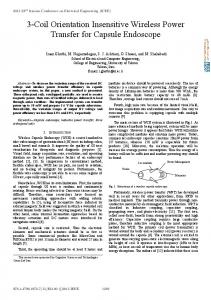
Effective Power Amplifier of Wireless Power Transfer System for Consumer Electronics Muhammad Ali
Hermawan Nugroho
Institute of Graduate Studies (IGS), SEGi University Kota Damansara, Malaysia
[email protected]
Faculty of Engineering and the Built Environment, SEGi University Kota Damansara, Malaysia
[email protected]
Abstract—Wireless power transfer (WPT) consists of three major parts namely transmitter, medium and receiver. In WPT system, input power is fed to the source where it transmits and propagates via coils and delivered to the load side. For an efficient operation of the WPT system, it is important to have a good power efficiency mechanism from the input to the transmitter coil. In this paper, a simulated design of power amplifier (PA) is introduced to improve the transmitter side of the WPT system (from input to transmitter coil). Optimum setting of Class E power amplifier that can be applied to portable power chargers available in the market is studied. GaN transistor with shunt capacitor is used due to its high efficiency and low resistance between drain and source. Results show that the proposed designs achieve 91% efficiency indicating a promising result. Index Terms-Class E power amplifier, GaN FET, High frequency, Wireless power transmission.
I.
INTRODUCTION
In recent years wireless power transfer (WPT) technology has gained high attention. According to LexInnova [1], WPT technology can generate 12 billion dollars revenue by 2020. The need for consumer and industrial electronics with WPT technology is reported to arise constantly. WPT setup basically consists of a transmitter with a source and transmitter coils, and a receiver with receiver coils and load. The transmitter and receiver coils are detached via medium (air). Various methods are introduced to transmit energy from transmitter side to the receiver such as microwave power transmission, magnetic and electromagnetic coupling [2]. Microwave transmission is commonly used for large distance (more than 20 kilometers). However, due to its omnidirection nature, the system efficiency is low [3]. Magnetic coupling is also not preferred as it operates in KHz (less than 500 KHz) frequency which will generate high parasitic effect. In addition, low frequency will also require large implication coils that increase the size and weight of the WPT system [4]. According to Shoki [5], WPT system with electromagnetic
coupling can obtain high efficiency in the ranges of 70% to 90%. Electromagnetic coupling can also operate in high frequency. High frequency will create strong coupling effect between transmitter and receiver with smaller coils resulting lighter and smaller WPT systems. According to previous works [6]–[15],amplifiers/rectifiers can be added in a WPT topology to improve efficiency of transmitter side of WPT system and thus, improving overall efficiency. Chen [4] reported that switching mode power amplifiers can be used in a WPT setup as it converts DC to AC and acts as inverter.. It is reported that mostly, Class E and Class DE switching mode power amplifiers are used as they have ideally 100% efficiency [6]–[15]. However, Class DE power amplifier uses two transistors with push-pull method which produces a high gate drive and it is hard to control the dead time. Therefore, it is hard to implant a Class DE power amplifier on a printed circuit board (PCB) [10]. Moreover, adding two transistors will increase the cost. Taking these into our consideration, in this paper, we study and use Class E power amplifier to improve efficiency of power transfer from input to the transmitter coil of WPT system. II. APPROACH Class E power amplifier consists of a switching mode transistor (GaNFET), a shunt capacitor (Cs), RF choke (L1), series LC circuit resonator (L2 and C2) and a load (R). When DC voltage is supplied through L1, it allows constant DC current and has zero resistance in switching mode power amplifier. In conventional classes of operation, switching mode power amplifier’s transistor acts as an ON/OFF switch. When the switch is ON, AC current flows into the transistor and when the switch is OFF, current flows into the load which causes a voltage. Ideally, this operation results with almost no overlap between voltage and current. However, this circuit topology has less efficiency. The efficiency reduces because lots of power dissipated at the harmonic frequencies not being transmitted through the fundamental. This can be improved by setting up a LC resonator circuit at the output
978-1-4673-8848-1/16/$31.00 ©2016 IEEE
side to control the harmonics. LC resonator blocks fundamental and allow all the other harmonics. The action of being ON and OFF of the switch will force a sinusoidal current to flow through the circuit. However, when the switch is ON, AC current will flow out of the LC resonator into the switch but when the switch is OFF, LC resonator pulls back the current from the switch to make a sine wave. There is no path for this current to return which can be solved by adding a capacitor in parallel to the switch. When the switch is OFF, current will return back to the resonator through the capacitor. Sinusoidal current wave form alternate flowing between the switch and the capacitor [16]. This setup has the potential to be 100% efficient ideally. In previous works Chen et al [4], replaced the shunt capacitor to reduce the size of the PA. We found however this setup will reduce the overall efficiency of the PA. Hence, in our work we include the shunt capacitor. A simple schematic of Class E power amplifier used in our simulation design is shown in Figure 1.
in weight. Each component’s values is driven through particular formula. According to Sokal [21], Class E power amplifiers has the following values, 0.577 × Vdc 2
Rl =
Pout
In his work, Srimuang et al [17] used Grebennikov’s formula [22] to obtain load resistance (Rl). According to Sokal [21], this value will change if the shunt capacitor is used in parallel. Hence, in our simulation, we follow Sokal’s formula.
Cs =
Ls =
1 wR × 5.447
1.1525 × R
LC =
w
1 2 w
L0 =
In this paper, we used high efficient GaN-FET switching mode transistor instead of commonly used silicon MOSFET. Si-MOSFETs are generally used for low frequencies and it shows high capacitance while operating in switching frequency. GaN-FET has low capacitance and shows low capacitance in switching frequency than Si-MOSFET [4]. Moreover, GaN FET has high operating temperature. In their previous works, Chen et al [4] and Srimuang et al [17] uses 25 V and 32 V drain voltages respectively. However, 32 V and 25 V DC is hard to supply from a portable battery. In our experiments, we find that lowering drain voltage will decrease the efficiency ( e.g. Witricity [18] achieves only 72% efficiency while supplying 12 V). Moreover, most of the smart phones nowadays use 5 V with 2 A (10 W) to charge their battery. Portable power banks which are available in markets has also similar output configuration (10W) [19]. Therefore, we keep 5 V drain voltage. We used EPC2022 model which is designed and manufactured by EPC Company [20]. The model has high drain voltage of 100 V with Rds(ON) only 3.2 mΩ which helps to decrease the parasitic capacitance. The smaller size of the transistor (6.05 mm × 2.3 mm) helps the prototype to become small and light
(2)
(3)
(4)
According to Grebennikov [22], 1 C0 = wQR
Figure 1. Basic schematic of Class E power amplifier (PA)
(1)
1 2 w C
(5)
(6)
Using equation 1, we can obtain Rl by setting up the output power. For example, if we set the output power to 10 W. This is based on electronic products that can charge smart phone and can be found easily in the market. Generally smart phones have supply voltage of 5 V. Therefore, to obtain 10 W output power, we supply 5 V drain voltage with 1.4425 Ω load resistance. Cs=1493.782 pF and Ls=19.513 nH are then calculated using Equations 2 and 3 respectively. However, the value of Ls mentioned in Chen’s [4] work is hard to find using equation (3). Next, the LC circuit resonator’s value is calculated using Equation 4. In our work, Q factor is included while calculating the L2 and C2 from the LC value. In previous work, Srimuang et al [17] set the Q factor as Q≈1 and Chen et al [4] do not specified the value of Q. Sokal suggested that Q must be greater or equal to 1.7879[21],. Therefore, we obtain L2= 9.4695 nH and C2= 14.5475 nF using Q=1.7879. These values are shown in Table 1. In the simulation, we varied input voltages and calculated the efficiency. A high frequency of 13.56 MHz with 5 V gate voltage was generated on gate driver.13.56 MHz was selected as a standard using industrial, scientific and medical (ISM) bands [23]. The simulation values are shown in the Table 1.
TABLE 1. THE INPUT AND OUTPUT POWER WITH EFFICIENCY IS COMPARISON VIA ACTUAL AND ROUND OFF VALUES
Parameters
Round off Values
Calculated Values
V1 (V)
5
5
V2 (V)
5
5
L1 (nH)
19.5
19.512
C1 (pF)
1500
1493.782
L2 (nH)
9.5
9.469
C2 (nF)
14.5
14.547
R
1.5
1.442
13.56
13.56
(Ω)
Frequency (MHz)
simulation, the input ranges from 5 W to 15 W, we get the following graph which is shown in Figure 2.
Figure 2. Plot of efficiency
III. RESULTS AND DISCUSSION Simulation is performed using LTspice IV. Table 2 shows the simulation with varied settings. It shows that simulation results show high resemblance with calculated results. TABLE
2. COMPARISON BETWEEN IDEAL AND SIMULATED RESULTS
Ideal Case
Simulated results
100%= Pout/Pin
Pin (W)
Pout (W)
Efficiency (%)
5w
5.77
4.94
85.615
6w
6.66
5.81
87.237
7w
7.6
6.76
88.947
8w
8.57
7.72
90.082
9w
9.61
8.68
90.323
10w
10.68
9.77
91.479
11w
11.8
10.82
91.695
12w
12.9
11.83
91.705
13w
14.04
12.9
91.880
14w
15.14
13.9
91.810
15w
16.23
14.9
91.805
In simulation design, the drain voltage V1 is constant. To obtain desired power, voltage and current must be known. In our work, we set V1 equal to 5 V. However, due to power dissipation in harmonics and switching loss, it is difficult to obtain exact power. As shown in Table 2, we obtain power input, Pin, of 10.679 W, and power output, Pout, of 9.769 W indicating 91.48% efficiency. We also perform simulation with rounded value based on the availability of the electronic components in the market. The rounded value simulation has power input of 10.473 W and power output of 9.549 W indicating 91.21% efficiency. Using equations 1 to 6, we obtained different values for L1, L2, C1, C2 and R for different ranges of input. In the
As shown in Figure 2, the output power and efficiency of the system are increasing exponentially and stabilizes after 9 W to 10 W. This indicates that our simulation (10 W) is already optimized for this particular settings. We observed that changing output power can affect every component of the circuit. As we increased the output power from 5 W to 15 W, the resistance and inductance (L1 and L2) increased while capacitance (C1 and C2) decreased. Figure 3 shows waveform of drain voltage V 1 (V(n002)) and gate voltage V 2 (V(n005)) of the system. It can be observed that V(n002) is off-nominal due to capacitance and inductance of C2 and L2 respectively . According to Sokal [21], we can improve it by increasing C2 and L2.
Figure 3. Drain and gate waveforms using LTspice. V(n002) waveform indicates voltage at the drain and V(n005) waveform shows the gate voltage when supply voltage is 5 V
The output current and voltage waveforms at load resistor R1 are shown in Figure 4. The ideal resistor should have in phase voltage and current waveform. As shown in Figure 4, the wavelength has a phase shift. This is due to parasitic capacitance and inductance influence [4].
The switch will be turned ON only when the gate voltage is 4 V or higher than 4 V. The results indicate that as the input increases, the efficiency of the amplifier increases gradually. However, increasing the gate voltage from 5V can cause harm to the transistor and burn the transistor. Therefore, we use 5 V gate voltage to turn ON the transistor. Table 3 shows the comparison between previous works and our proposed design. TABLE
3. EFFICIENCY OF THE PROPOSED WPT Efficiency
Figure 4. Voltage and current waveforms at load resistor R1 with supply voltage of 5 V using LTspice. V(n004) waveform shows the voltage supplied and I(R1) waveform indicates current wavelength
Additionally, we calculate the efficiency by changing V1 while other values were kept constant. According to Figure 5, the efficiency increases gradually as drain voltage is increased. Moreover, the output power is also increased. On the other hand, in the drain voltage and all other parameters were kept constant and different gate voltage is supplied.
References
Input Voltage
Kender et al [8]
5V
67%
-
Witricity [18]
5V
78%
-
Witricity
12 V
86%
72%
Witricity
5V
84%
-
End to End Efficiency
Efficiency
According to Table 3, Witricity [18] reported the highest end-to-end efficiency of 86% with 72% efficiency at the transmitter side of the WPT system. In our work, we obtain 91% efficiency. This shows that our design is promising and has the potential to be used for actual WPT system. Overall end-to-end WPT system efficiency depends on the efficiency of power amplifier. The input power is supplied to the transmitter side of WPT where it is inverted from DC to AC using power amplifier. As a result, optimum end-to-end power transfer can only be achieved with an effective power amplifier. IV. CONCLUSION
Figure 5. Plot of efficiency versus Pout of the Class E power amplifier, when Vdd is increased from 1 V to 12 V
As shown in Figure 6, the efficiency is increasing by increasing gate voltage.
Figure 6. Indicates the change in efficiency and output power when the gate voltage is supplied from 4 V to 6 V
In this paper an improvement method for wireless power transfer (WPT) is proposed. According to LexInnova [1], the need for WPT for charging consumer electronics is increasing. Thus, a high end-to-end efficiency of WPT system is anticipated. WPT system consists of three major parts namely transmitter, medium and receiver. Researchers reported that WPT system can be improved by implementing power amplifiers in the transmitter side of the system. By improving efficiency on the transmitter side, we improve the end-to-end efficiency of the system. In our work, we design and implement Class E power amplifier to improve the transmitter side of WPT system. The system is developed under the assumption that it will be used to charge consumer electronics (smart phones) available in the market. The design is tested and simulated using LTspice. Results show that the design achieves 91% efficiency. This indicates that the proposed design has the potential to be used for actual WPT system. For future work, we will design a prototype system based on our proposed simulation.
REFERENCES [1] [2] [3] [4]
[5]
[6] [7] [8]
[9] [10]
[11]
[12] [13]
“Wireless Power Transmission: Patent Landscape Analysis.” X. Lu, P. Wang, D. Niyato, D. I. Kim, Z. Han, and C. Engineering, “Wireless Charging Technologies : Fundamentals , Standards , and Network Applications,” no. c, pp. 1–41, 2015. S. Y. R. Hui, W. Zhong, and C. K. Lee, “A Critical Review of Recent Progress in Mid-Range Wireless Power Transfer,” IEEE Trans. Power Electron., vol. 29, no. 9, pp. 4500–4511, 2014. W. Chen, R. A. Chinga, S. Yoshida, J. Lin, C. Chen, W. Lo, I. Technology, and N. E. C. Corporation, “A 25 . 6 W 13 . 56 MHz Wireless Power Transfer System with a 94 % Efficiency GaN Class-E Power Amplifier,” IEEE, pp. 25–27, 2012. J. H. Shoki ; Corp. R&D Center, Toshiba Corp., Kawasaki, “Issues and initiatives for practical use of wireless power transmission technologies in Japan,” Microw. Work. Ser. Innov. Wirel. Power Transm. Technol. Syst. Appl. (IMWS), 2011 IEEE MTT-S Int., no. IEEE, pp. 87 – 90, 2011. J. Tan, S. Member, C. Heng, and Y. Lian, “Design of Ef fi cient Class-E Power Ampli fi ers for Short-Distance Communications,” IEEE, vol. 59, no. 10, pp. 2210–2220, 2012. I. D. de Vries, J. H. van Nierop, and J. R. Greene, “Solid state class DE RF power source,” IEEE Symp. Ind. Elcron., pp. pp. 524–529, 1998. G. A. Kendir, W. Liu, G. Wang, M. Sivaprakasam, R. Bashirullah, M. S. Humayun, and J. D. Weiland, “An optimal design methodology for inductive power link with Class-E amplifier,” IEEE Trans. Circuits Syst. I Regul. Pap., vol. 52, no. 5, pp. 857– 866, 2005. H. Sekiya, H. Koizumi, S. Mori, I. Sasase, J. Lu, and T. Yahagi, “FM/PWM Control Scheme in Class DE Inverter,” IEEE Trans. Circuits Syst. I Regul. Pap., vol. 51, no. 7, pp. 1250–1260, 2004. R. J. Calder, S.-H. Lee, and R. D. Lorenz, “Efficient, MHz frequency, resonant converter for sub-meter (30 cm) distance wireless power transfer,” Energy Convers. Congr. Expo., no. 30 cm, pp. 1917–1924, 2013. S. M. Abbas, M. A. Hannan, and A. S. Salina, “Efficient Class-E Design for Inductive Powering Wireless Biotelemetry Applications Efficient Class-E Design for Inductive Powering Wireless Biotelemetry Applications,” no. FEBRUARY 2012, 2016. T. Chan, C. Chen, and S. Member, “Transmission System,” vol. 59, no. 8, pp. 1805–1814, 2012. M. Fu, S. Member, H. Yin, S. Member, and X. Zhu, “Analysis and Tracking of Optimal Load in Wireless Power Transfer Systems,”
[14]
[15] [16]
[17] [18]
[19] [20]
[21] [22] [23]
pp. 1–12, 2014. T. Nagashima, X. Wei, and H. Sekiya, “Analytical design procedure for resonant inductively coupled wireless power transfer system with class-E inverter and class-DE rectifier,” 2014 IEEE Asia Pacific Conf. Circuits Syst., pp. 288–291, 2014. F. H. Raab, “Idealized Operation of the Class E Tuned Power Amplifier,” IEEE Trans. Circuits Syst., vol. 24, no. 12, pp. 725– 735, 1977. Y. Kamito, K. Fukui, and H. Koizumi, “An Analysis of the Class-E Zero-Voltage-Switching Rectifier Using the Common-Grounded Multistep-Controlled Shunt Capacitor,” IEEE Trans. Power Electron., vol. 29, no. 9, pp. 4807–4816, 2014. P. Srimuang, N. Puangngernmak, and S. Chalermwisutkul, “13 . 56 MHz Class E Power Amplifier with 94 . 6 % Efficiency and 31 Watts Output Power for RF Heating Applications,” 2014. “WiT-2000M Developer Kit for Mobile Devices WiTricity for Mobile Devices Highly Resonant Wireless Power Transfer has arrived.” [Online]. Available: http://www.witricity.com/assets/WiT-2000M-developers-kit-formobile-data-sheet-v141.pdf. [Accessed: 22-May-2016]. “MI.” [Online]. Available: http://www.mi.com/sg/pb10000/#params. [Accessed: 22-May2016]. “EPC2022 - Enhancement Mode Power Transistor.” [Online]. Available: http://epcco.com/epc/Products/eGaNFETs/EPC2022.aspx. [Accessed: 25Apr-2016]. N. O. Sokal, “Class-E RF Power Amplifiers,” Notes, vol. 204, no. 204, pp. 9–20, 2001. A. V Grebennikov, H. Jaeger, M. A. E. Operations, and L. T. Park, “HIGH-EFFICIENCY RF ’ AND MICROWAVE POWER AMPLIFIERS,” pp. 1627–1630, 2002. “ISM Bands.” [Online]. Available: http://www.itu.int/dms_pub/itus/oth/02/02/S02020000184501PDFE.PDF. [Accessed: 22-Apr2016].