582
IEEE ELECTRON DEVICE LETTERS, VOL. 31, NO. 6, JUNE 2010
Efficiency Improvement of GaN-Based LEDs With a SiO2 Nanorod Array and a Patterned Sapphire Substrate H. W. Huang, J. K. Huang, C. H. Lin, K. Y. Lee, H. W. Hsu, C. C. Yu, and H. C. Kuo
Abstract—The enhancement of light extraction from GaNbased light-emitting diodes (LEDs) with a patterned sapphire substrate (PSS) and a SiO2 12-fold photonic quasi-crystal (PQC) structure using nanoimprint lithography is presented. At a driving current of 20 mA on transistor-outline-can package, the light output powers of LED with a PSS and LED with a PSS and a SiO2 PQC structure are enhanced by 35% and 48%, compared with the conventional LED. In addition, the higher output power of the LED with a PSS and a SiO2 PQC structure is due to better reflectance on PSS and higher epitaxial quality on an n-GaN using a SiO2 12-fold PQC structure pattern. These results provide promising potential to increase output powers of commercial light-emitting devices. Index Terms—Gallium nitride (GaN), light-emitting diodes (LEDs), nanoimprint lithography (NIL), patterned sapphire substrate (PSS).
I. I NTRODUCTION
T
O REALIZE high brightness, gallium nitride (GaN)-based light-emitting diodes (LEDs) have made possible their use in large-size flat-panel displays [1], [2]. However, there is still a great need to improve the internal quantum efficiency (IQE) and external quantum efficiency (EQE) in order to increase the light output performance and thus reduce the total cost of LED modules. Further improvement in the EQE of a GaNbased LED on a patterned sapphire substrate (PSS) is required. In addition, high-quality GaN-based LEDs are affixed onto a microscale PSS [3], [4]. The microscale patterns serve as a template for the epitaxial lateral overgrowth (ELOG) of GaN and the scattering centers for the guided light. Both the epitaxial crystal quality and the light extraction efficiency are improved by utilizing a microscale PSS. In the epitaxial growth method, a number of attempts have been made to reduce the dislocation effect using such strategies as the insertion of a microscale epitaxial ELOG layer of SiO2 or a Six Ny pattern on the GaN thin film [5]–[7]. However, they are typically fabricated by photolithography or self-assembly. To fabricate them more easily, one candidate method is nanoimprint lithography (NIL). Manuscript received January 24, 2010; revised March 7, 2010. Date of publication April 15, 2010; date of current version May 26, 2010. The review of this letter was arranged by Editor C. Jagadish. H. W. Huang, J. K. Huang, and H. C. Kuo are with the Institute of ElectroOptical Engineering, National Chiao Tung University, Hsinchu 300, Taiwan (e-mail:
[email protected];
[email protected]; haochung_
[email protected]). C. H. Lin, K. Y. Lee, H. W. Hsu, and C. C. Yu are with Unilite Corporation, Miaoli 350, Taiwan (e-mail:
[email protected];
[email protected];
[email protected]). Color versions of one or more of the figures in this letter are available online at http://ieeexplore.ieee.org. Digital Object Identifier 10.1109/LED.2010.2045472
Fig. 1.
Schematic diagram of LED with a PSS and a SiO2 PQC structure.
In this letter, we utilize a nanoimprinting technique to fabricate a microscale PSS and a SiO2 photonic quasi-crystal (PQC) structure on n-GaN layer to be used for mass production. As a result, the light output efficiency of LED with a PSS and a SiO2 PQC pattern on n-GaN layer is significantly higher than that of a conventional LED. II. E XPERIMENTS Fig. 1 shows the schematic diagram of GaN-based LED with a PSS and a SiO2 PQC structure pattern. In our study, two types are fabricated in order to investigate the influence the PSS and a SiO2 PQC structure on n-GaN layer has on the LED output power and beam profile performance. In Fig. 1, the LED structure consists of a Cr/Pt/Au p-electrode, an ITO transparent layer, a LED epitaxial layer, a smooth p-GaN surface, and a Cr/Pt/Au n-electrode on PSS structure. Furthermore, the LED epitaxial structure has inset a SiO2 PQC pattern on an n-GaN layer by NIL. The following details the process flow of NIL on a sapphire substrate. First, we spin coat a 600-nm polymer layer on the sapphire sample surface. Second, we place a patterned mold onto the dried polymer film. By applying high pressure, we can heat the sapphire substrates to above the glass transition temperature of the polymer. Third, the sapphire substrates and the mold are cooled down to room temperature to release the mold. Finally, we use inductively coupled plasma reactive ion etching (RIE) with BCl3 plasma to transfer the pattern onto the sapphire substrate and remove the polymer layer with O2 plasma etching gas in a RIE system. Fig. 2(a) shows the 45◦ tilt view of atomic force microscope (AFM) image on substrate with a PSS. The AFM image [Fig. 2(a)] shows the triangular lattice of PSS with cones, which is defined by NIL. The lattice constant (a) of PSS structure is 3 µm, and the cone diameter d (2.5 µm) is fixed to ratio d/a = 0.83. However, the AFM
0741-3106/$26.00 © 2010 IEEE
HUANG et al.: EFFICIENCY IMPROVEMENT OF GaN-BASED LEDS
583
Fig. 2. AFM images of (a) 45◦ tilt view of sapphire surface with a PSS and (b) 45◦ tilt view of n-GaN surface with a SiO2 PQC. (Inset: The AFM image of 12-fold PQC pattern on an n-GaN surface with a SiO2 PQC structure.)
image shows the etching depth and sidewall angle of PSS to be approximately 700 nm and 29◦ , respectively. All LED samples are grown by MOCVD with a rotating-disk reactor (Veeco) on a c-axis sapphire (0001) substrate at a growth pressure of 200 mbar. The LED structure consists of a 50-nmthick GaN nucleation layer, a 3-µm-thick undoped GaN buffer layer, a 3.5-µm-thick Si-doped GaN layer, an unintentionally doped InGaN/GaN multiple quantum well (MQW) active region, a 50-nm-thick Mg-doped p-AlGaN electron blocking layer, and a 120-nm-thick Mg-doped p-GaN contact layer. The MQW active region consists of five periods of 3-nm/ 20-nm-thick In0.18 Ga0.82 N/GaN quantum well layers and barrier layers. The inset of a SiO2 layer of NIL process flow on an n-GaN layer is the same method with PSS process. First, we deposited a 200-nm-thick SiO2 layer and spin coat a 200-nm polymer layer on a GaN epitaxial sample surface. Second, we place a patterned mold onto the dried polymer film. By applying high pressure, we can heat the LED samples to above the glass transition temperature of the polymer. Third, the LED samples and the mold are cooled down to room temperature to release the mold. Finally, we use an RIE with CF4 plasma to transfer the pattern onto the GaN sample and remove the polymer layer with O2 plasma etching gas in RIE system. Fig. 2(b) show the 45◦ tilt view of an AFM with 12-fold PQC pattern based on a square–triangular lattice. The Fig. 2(b) inset image shows the top-view AFM image of 12-fold PQC pattern. We choose the 12-fold PQC pattern due to the better enhancement of surface emission [8]. This is obtained from the photonic crystals (PhCs) with a dodecagonal symmetric quasicrystal lattice, as opposed to regular PhCs with triangular lattice and eightfold PQC pattern [8]. The recursive tiling of offspring
Fig. 3. (a) Current–voltage (I–V ) characteristics of conventional LED, LED with a PSS, and LED with a PSS and a SiO2 PQC structure. (b) Intensity– current (L–I) characteristics of conventional LED, LED with a PSS, and LED with a PSS and a SiO2 PQC structure.
dodecagons packed with random ensembles of squares and triangles in dilated parent cells forms the lattice. The “PQC” is unusual because, on first sight, they appear random; however, a closer inspection reveals them to possess long-range order but short-range disorder. The lattice constant and rod diameters are 750 and 400 nm, respectively. Furthermore, in Fig. 2(b), the SiO2 PQC depth of the n-GaN layer is set to be approximately 200 nm. In this study, our LED samples are fabricated using the following standard processes with a mesa area of 300 × 300 µm2 . The detail of the standard process is described in [9]. III. R ESULTS Fig. 3(a) shows the characteristics of typical current–voltage (I–V ). It is found that the measured forward voltages under an injection current of 20 mA at room temperature for conventional LED, LED with PSS, and LED with a PSS and a SiO2 PQC structure are 3.16, 3.15, and 3.23 V, respectively. In addition, the dynamic resistances of conventional LED, LED with a PSS, and LED with a PSS and a SiO2 PQC structure are about 14.7, 15.3, and 15.4 Ω, respectively. Therefore, in terms of dynamic resistance, there is no influence on this type of devices by incorporating PSS and a SiO2 PQC structure by NIL process. The light output is detected by calibrating an integrating sphere with Si photodiode on the package device, so that the light emitted in all directions from the LED can be collected. The intensity–current (L–I) characteristics of conventional
584
IEEE ELECTRON DEVICE LETTERS, VOL. 31, NO. 6, JUNE 2010
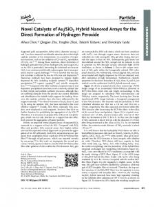
Fig. 5. TEM image of GaN/sapphire interface for the GaN epilayer grown on a PSS and a SiO2 PQC structure.
IV. C ONCLUSION Fig. 4. Arrhenius plots of integrated PL intensities for GaN-based LED with/without a PSS and a SiO2 PQC structure on n-GaN layer.
LED, LED with a PSS, and LED with a PSS and a SiO2 PQC structure are shown in Fig. 3(b). At an injection current of 20 mA and a peak wavelength of 460 nm for a transistor outline (TO)-can package, the light output powers of conventional LED, LED with a PSS, and LED with a PSS and a SiO2 PQC structure on TO-can are 8.5, 11.5, and 12.6 mW, respectively. Hence, the enhancement percentages of LED with a PSS, and LED with a PSS and a SiO2 PQC structure are 35%, and 48%, respectively, compared to that of conventional LED. The higher enhancement from standard LED type is due to the effect of the PSS, which allows the light to reflect from the sapphire substrate onto the top direction. In addition, the use of a 12-fold SiO2 PQC pattern results in higher epitaxial crystal quality [5]–[7], which increases more light output power. In addition, the corresponding wall plug efficiencies of conventional LED, LED with a PSS, and LED with a PSS and a SiO2 PQC structure are 13%, 18%, and 20%, respectively. This is a substantial improvement for the PSS and a SiO2 PQC structures as well. Fig. 4 shows that temperature-dependent photoluminescence (PL) used to determine the IQE of the InGaN/GaN MQW structures. At low temperatures, the nonradiative recombination is close to minimum and radiative recombination processes are dominant. With increasing temperature, nonradiative recombination processes get activated and play a key role at room temperature [11]. We obtain an IQE of LED with a PSS and a SiO2 PQC to be higher (41%) than that of the conventional LED (33%) at room temperature. Therefore, the LED with a PSS and a SiO2 PQC structure has higher epitaxial crystal quality due to the improved IQE performance on LED structure. Transmission electron microscopy (TEM) was employed to investigate the crystalline quality of GaN layers that are epitaxially grown on a PSS and a SiO2 PQC structure in Fig. 5. The crystalline quality of GaN epilayer on a SiO2 PQC structure was improved from that grown on a PSS. It is believed that the presence of stacking faults could block the propagation of threading dislocations (TDs) [7]. Moreover, the TDs of the GaN layer on a PSS mainly originated from an exposed sapphire surface, which could be bent due to the lateral growth of GaN. In addition, the dislocation bending with visible turning points [7] and, according to the works of Park et al., the enhancement of efficiency may be due to the increase of the light extraction through the top surface by embedded air-void structure [10].
GaN-based LEDs with a PSS and a SiO2 PQC structure have been fabricated and demonstrated. At a driving current of 20 mA on a TO-can package, the light output power of LEDs with a PSS and a SiO2 PQC structure is enhanced by a factor of 1.48. The higher output power of the LED with a PSS and a SiO2 PQC structure is due to the higher reflectance on PSS and higher epitaxial quality on n-GaN layer using a SiO2 12-fold PQC pattern. This letter offers promising potential to increase output powers of commercial light-emitting devices. R EFERENCES [1] M. Koike, N. Shibata, H. Kato, and Y. Takahashi, “Development of high efficiency GaN based multiquantum-well light-emitting diodes and their applications,” IEEE J. Sel. Topics Quantum Electron., vol. 8, no. 2, pp. 271–277, Mar./Apr. 2002. [2] E. F. Schubert, Light-Emitting Diodes. Cambridge, U.K.: Cambridge Univ. Press, 2003. [3] T. S. Oh, S. H. Kim, T. K. Kim, Y. S. Lee, H. Jeong, G. M. Yang, and E. K. Suh, “GaN-based light-emitting diodes on micro-lens patterned sapphire substrate,” Jpn. J. Appl. Phys., vol. 47, no. 7, pp. 5333–5336, 2008. [4] D. S. Wuu, W. K. Wang, K. S. Wen, S. C. Huang, S. H. Lin, R. H. Horng, Y. S. Yu, and M. H. Pan, “Fabrication of pyramidal patterned sapphire substrates for high-efficiency InGaN-based light emitting diodes,” J. Electrochem. Soc., vol. 153, no. 8, pp. G765–G770, 2006. [5] H. Gao, F. Yan, Y. Zhang, J. Li, Y. Zeng, and G. Wang, “Enhancement of the light output power of InGaN/GaN light-emitting diodes grown on pyramidal patterned sapphire substrates in the micro- and nanoscale,” J. Appl. Phys., vol. 103, no. 1, pp. 014 314-1–014 314-5, Jan. 2008. [6] J. J. Chen, Y. K. Su, C. L. Lin, S. M. Chen, W. L. Li, and C. C. Kao, “Enhanced output power of GaN-based LEDs with nano-patterned sapphire substrates,” IEEE Photon. Technol. Lett., vol. 20, no. 13, pp. 1193–1195, Jul. 2008. [7] C. H. Chiu, H. H. Yen, C. L. Chao, Z. Y. Li, P. C. Yu, H. C. Kuo, T. C. Lu, S. C. Wang, K. M. Lau, and S. J. Cheng, “Nanoscale epitaxial lateral overgrowth of GaN-based light-emitting diodes on a SiO2 nanorod-array patterned sapphire template,” Appl. Phys. Lett., vol. 93, no. 8, pp. 081 108-1– 081 108-3, Aug. 2008. [8] Z. S. Zhang, B. Zhang, J. Xu, K. Xu, Z. J. Yang, Z. X. Qin, T. J. Yu, and D. P. Yu, “Effects of symmetry of GaN-based two-dimensional photonic crystal with quasicrystal lattices on enhancement of surface light extraction,” Appl. Phys. Lett., vol. 88, no. 17, pp. 171 103-1–171 103-3, Apr. 2006. [9] H. W. Huang, C. H. Lin, J. K. Huang, K. Y. Lee, C. C. Yu, and H. C. Kuo, “Improved light output power of GaN-based light-emitting diodes using double photonic quasi-crystal patterns,” IEEE Electron Device Lett., vol. 30, no. 11, pp. 1152–1154, Nov. 2009. [10] E. H. Park, J. Jang, S. Gupta, I. Ferguson, C. H. Kim, S. K. Jeon, and J. S. Park, “Air-voids embedded high efficiency InGaN-light emitting diode,” Appl. Phys. Lett., vol. 93, no. 19, pp. 191 103-1–191 103-3, Nov. 2008. [11] S. Watanabe, N. Yamada, M. Nagashima, Y. Ueki, C. Sasaki, Y. Yamada, T. Taguchi, K. Tadatomo, H. Okagawa, and H. Kudo, “Internal quantum efficiency of highly-efficient InxGa1-xN-based near-ultraviolet light-emitting diodes,” Appl. Phys. Lett., vol. 83, no. 24, pp. 4906–4908, Dec. 2003.