48.3
Efficient and Accurate Gate Sizing with Piecewise Convex Delay Models Hiran Tennakoon and Carl Sechen Department of Electrical Engineering University of Washington, Seattle WA 98195-2500
[email protected],
[email protected] Second, it is important for the sizer to generate solutions at least close to optimum. An important contribution made in TILOS is the observation that Elmore delay is convex under a variable transformation x = e z [5]. For a convex function any local optimum is also a global optimum. However, their formulation of the problem, and the sensitivity-based heuristic, cannot guarantee optimal results. The complex models used by Sapatnekar et al. are convex, and they use an interior-point algorithm to find optimum solutions [9]. However, without correct delay propagation, the practicality of their algorithm is in question. Further, the interior point algorithm is prone to large run-times [10]. Chen et al. first formulated the gate-sizing problem in an elegant mathematical form that was solvable with guarantees of optimality [11]. Though they used the Elmore delay model in their work, their formulation of the sizing problem is very significant, as it enabled optimization to be carried out on the entire design rather than optimization of only the critical paths of the design. However, in [12] it is shown that the convergence of the algorithm used is highly sensitive to initial conditions and constant factors. Third, it is important that the sizing algorithm is efficient, especially given the ever-larger circuits. Approaches such as JiffyTune [13] and EinsTuner [14] use dynamic timing engines to generate circuit sensitivities and thus incur large run-time penalties. While JiffyTune uses dynamic timing analysis, generating exact solutions, EinsTuner uses static timing analysis with the latestarrival delay propagation method and has additional slew-rate constraints at each node in the design. Further, most sizing algorithms do not use accurate delay propagation for multi-input gates. Two possible methods of delay propagation for multi-input gates are the latest arrival propagation, and the worst slew propagation. While the first approach is too optimistic, the later is too pessimistic. This work addresses each of the three above issues. We form our delay models by characterizing a library of gates, with maximum and minimum limits on the sizes of transistors. Each gate in the library has minimum/maximum beta ratio limits. All gates are treated as parameterized cells, with one variable controlling the width of the nMOS transistors, and another controlling the pMOS transistors. We generate a piecewise convex delay model by efficiently dividing the measured data into smaller regions; thus, we show great improvement in the accuracy and range (in terms of output load and slew-rate) of the model. The delay model is dependent on input slew-rate, transistor sizes, and output loading. While we can only prove convexity on each individual piece, and not the overall model, our sizing algorithm, called Forge, exhibits optimality. Our static timing analyzer uses a realistic delay propagation method that uses a combination of the arrival times and their slewrates to determine delay propagation. The rest of the paper is organized as follows. In Section 2 we will formulate the problem and address algorithmic issues. Then in Section 3 we present the piecewise convex delay model and how it
ABSTRACT We present an efficient and accurate gate sizing tool that employs a novel piecewise convex delay model, handling both rise and fall delays, for static CMOS gates. The delay model is used in a new version of a gate-sizing tool called Forge, which not only exhibits optimality, but also efficiently produces the area versus delay tradeoff curve for a block in one step. Forge includes a realistic delay propagation scheme that combines arrival times and slew-rates. Forge is 6.4X faster than a commercial transistor sizing tool, while achieving better delay targets and uses 28% less transistor area for specific delay targets, on average.
Categories and Subject Descriptors B.7.2 [Integrated Circuits]: Design Aids.
General Terms Design, Performance, Algorithms
Keywords Delay modeling, gate sizing, Lagrangian relaxation, piecewise convex, optimization
1
INTRODUCTION
Automation of the transistor sizing process has been steadily gaining popularity in digital/analog VLSI design. Using modeling techniques, many automation algorithms guarantee globally optimum solutions for given specifications [1]. In digital CMOS design, sizing enables one to evaluate the performance of different cell libraries [2], to address the timing closure problem when the design is placed and routed [3], and to generate area/power versus delay trade-off curves [4]. The usefulness of a transistor or gate sizer depends on three issues: delay model accuracy, optimality and efficiency. First, the models used must be accurate enough to provide useful solutions to the practical problem. TILOS [5], which was the first algorithmic attempt at transistor sizing, used the popular Elmore delay model [6]. Sapatnekar et al. in their work on convex gate level delay models showed that in modern designs the average error of the Elmore model to Hspice is as much as 20.5% [7]. This renders the Elmore model unsuitable for optimization, as solutions will not correlate well with Hspice results. In the same work they present an input slew-rate dependent model with greater accuracy than Elmore [7]. Their approach is to run a gate level characterization using Hspice, over a range of device sizes, input slew-rates, and output loading. Then they fit this measured data to predefined convex functions. Permission to make digital or hard copies of all or part of this work for personal or classroom use is granted without fee provided that copies are not made or distributed for profit or commercial advantage and that copies bear this notice and the full citation on the first page. To copy otherwise, or republish, to post on servers or to redistribute to lists, requires prior specific permission and/or a fee. DAC 2005, June 13–17, 2005, Anaheim, California, USA. Copyright 2005 ACM 1-59593-058-2/05/0006…$5.00.
807
is integrated within the optimization framework. Section 4 will present results for 31 benchmarks, comparing Forge with a commercial transistor sizing tool (CTST). Conclusions will then follow in Section 5.
2
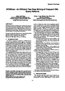
V dd o u tp u t o f slo w e r sk e w i n p u t V d d /2 s lo w e r sk ew inp ut
Problem Formulation
We are interested in the generation of the area versus delay trade-off curve for a logic block. The trade-off curve may be generated by a series of optimizations formulated as: Minimize f (w ) = ∑ wi
g nd fa ste r sk e w i n p u t
Figure 3. Shows an earlier arriving signal with a large slew-rate causing a later arrival signal at the output than the later arrival at the input.
(1)
subject to Delay ≤ Delaytarget
where the area is represented by the sum of transistor widths, wi. Delay is the maximum arrival time at any output. Sweeping the target delay (Delaytarget) generates the curve. This approach is used in [4]. The problem here is how to determine the incremental delay step that the target must be reduced by. Since the absolute best delay is unknown a priori, the optimizer may take many small time steps to generate the trade-off curve. Knowing the absolute minimum delay achievable greatly speeds up the process. Our approach is summarized in Figure 1.
The additional variable a0 facilitates the minimization of the maximum of the arrival times a7 and a8. Li and Ui are the lower and upper limits for the transistor widths, and these are simple boundary constraints. Note that for simplicity in the paper (but not in the implementation) the formulation here does not include wire capacitances, nor does it differentiate the delay functions in terms of nMOS and pMOS sizes, nor does it distinguish the rise/fall slew-rates. The formulation given in () uses the latest arrival method to propagate delay. This has been shown to create optimistic delays [8], as shown in Figure 3, where the earlier arriving signal with slower slew results in the latest arrival at the gate output. Propagating the worst slew-rate will result in the delay estimation being too pessimistic [8]. We use a variant of the half-envelope approach from [8], where we combine the delay with ¼ of the slew-rate to decide which signal to propagate. Introducing this to equation (): Minimize a0
Area vs. Delay Curve Generation: 1. Start with minimum sizes 2. Set Delaymax = Delay with minimum sizes 3. Solve for minimum delay possible for design 4. Set Delaymin = Delay after sizing 5. Set n Delay targets between Delaymax and Delaymin 6. Minimize Area for the n Delay targets
subject to : a7 ≤ a0
Figure 1. Approach to generate the area versus delay curve. a 1 , s1
a 2 , s2
D 15, S 15
a 5 , s5
D 57, S 57
D 25, S 25
a7
a + D15 if a1 + D15 + 1 4 S15 ≥ a2 + D25 + 1 4 S 25 a5 = 1 1 1 a2 + D25 if a2 + D25 + 4 S 25 > a1 + D15 + 4 S15 if a1 + D15 + 1 4 S15 ≥ a2 + D25 + 1 4 S 25 S s5 = 15 1 1 S 25 if a2 + D25 + 4 S25 > a1 + D15 + 4 S15
D 67, S 67
a 4 , s4
D 36, S 36
D 68, S 68
a8
a + D36 if a3 + D36 + 1 4 S36 ≥ a4 + D46 + 1 4 S46 a6 = 3 1 1 a4 + D46 if a4 + D46 + 4 S46 > a3 + D36 + 4 S36
D 46, S 46
S36 if a3 + D36 + 1 4 S36 ≥ a4 + D46 + 1 4 S46 s6 = 1 1 S46 if a4 + D46 + 4 S46 > a3 + D36 + 4 S36 (3) Li ≤ wi ≤ U i In equation (3), for each output except for the primary outputs, the arrival time is equal to the input arrival ai and gate delay Dij that maximizes the output arrival time, plus ¼ of the output slew-rate Sij. The same holds for the output slew-rates; we pick the slew-rate Sij of the input that maximizes the output delay and slew-rate combination. We take the latest arrival times at the primary outputs. We have a non-smooth problem, as there is an arbitration that determines which delay/slew-rate pair gets propagated. If we assume that the delay and slew-rate are correctly assigned, then we can rewrite (3) as: Minimize a0
Figure 2. Circuit fragment to aid formulation of the problem for the minimization of the maximum delay. Dij, Sij are the resulting gate input i to output j delay and output slew-rate, respectively. ai, si are the arrival time and slew-rate at output i.
2.1
Minimum Delay Formulation
For the circuit fragment given in Figure 2, the formulation of the minimization of the maximum delay at the primary outputs is given by (2). Minimize a0 subject to : a 7 ≤ a0
a8 ≤ a0
a5 + D57 ≤ a7
a6 + D67 ≤ a7
a6 + D68 ≤ a8 a2 + D25 ≤ a5
a1 + D15 ≤ a5 a3 + D36 ≤ a6
a4 + D46 ≤ a6
Li ≤ wi ≤ U i
a8 ≤ a0
a5 + D57 if a5 + D57 ≥ a6 + D67 a7 = a6 + D67 if a6 + D67 > a5 + D57 a8 = a6 + D68
a 6, s 6 a 3 , s3
o u tp u t o f fa st e r sk e w i n p u t
(2)
subject to : a7 ≤ a0
a8 ≤ a0
a5 + D57 ≤ a7
a6 + D67 ≤ a7
a6 + D68 ≤ a8
808
a1 + D15 + a2 + D25 + a3 + D36 +
1 4 S15 ≤ a5 + 4 s5 1 S ≤a +1 s 5 4 25 4 5 1 S 1 s ≤ a + 36 6 4 4 6 1 S 1 4 46 ≤ a6 + 4 s6
the required time. For all other gates the multiplier for each gate input i is updated by multiplying itself by the ratio of the current arrival time to input i, plus the input i to output j delay, plus ¼ of input i to output j slew, to the arrival time at output j plus ¼ the slew. Note that correct values for the output arrival time and slew rate have been chosen as given in (3). Consider the equation below.
1
(4)
a4 + D46 + For minimizing the worst-case primary output arrival time, we know from the Kuhn-Tucker optimality conditions on the arrival times that the sum of the Lagrange multipliers assigned to the primary outputs must be equal to one, and that the sum of multipliers at a gate’s input must equal the sum of the multipliers at the inputs of gates that are driven by that gate [11]. Further, if a set of λ’s are chosen such that they satisfy the optimality conditions then (4) reduces to:
f (x ) = 109 x12 + x22 (8) It can be seen that f(x) is extremely sensitive to changes in x1 and not x2. This is a poorly scaled problem and has a large impact on gradient-based approaches [17]. This problem can arise in our case when executing the delay-constrained area minimization phase. There we have the following form: L(w,λ ) = f (w ) + ∑ λi gi (w ) (9)
Minimize L(w, λ ) = λ68 D68 + λ67 D67 + λ57 D57
+ λ15 (D15 +
)
(
)
1 4 S15 + λ25 D25 + 4 S 25 1 + λ36 D36 + 4 S36 + λ46 D46 + 1 4 S 46
(
1
)
(
i
where f is the sum of sizes, λi are the Lagrange multipliers, and gi are the constraint functions. Note that in the first phase when the algorithm minimizes the maximum delay, f is not present, thus, no scaling is required. If we apply the variable transformation w = exp(z ) then f is convex. Multiplying by α (a positive variable) conserves convexity, and enables scaling between the area terms and the delay terms, as given below. (10) L(w, λ ) = αf (w ) + ∑i λi gi (w )
)
(5) subject to : Li ≤ wi ≤ U i Now the problem is reduced to finding the optimum sizes and the optimum values for the Lagrange multipliers λ. The optimum delays and slew-rates will be selected as shown in equation (3). For more details on applying Lagrangian relaxation to the gate-sizing problem the reader is directed to [11]. Once we obtain the minimum delay bound then we can minimize the area for given delay targets.
2.2
Initialize α = α0, k = 1, |∇L0| = ∞ while |∇Lk-1|-|∇Lk| ≥ tolerance do αk+1 = αk/10 k = k+1 end while
Delay Constrained Area Minimization
Consider the circuit fragment in Figure 2 again. Now we represent the area as the sum of transistor widths and solve the area minimization problem given in (1). By constraining all gate input to output arrival times as in (3) and using the Kuhn-Tucker optimality conditions on the arrival times we have the following formulation for area minimization given delay constraints. Minimize L(w, λ ) = ∑ wi + λ68 D68 + λ67 D67 + λ57 D67 + λ15 (D15 +
+ λ36 (D36 +
1
Figure 4. Algorithm to determine the scaling factor α. |∇Lk| is the norm of gradient of L at iteration k. α0=1e-3
When the minimum delay bound is found, we determine the α term as follows. Starting with a positive α, we determine the norm of the gradient of (10). Then we progressively decrease α, until the difference between the current norm and the previous is less than a threshold. We found that a tolerance of 0.1 was sufficient. As the algorithm proceeds, since the multiplier values are updated to prevent bad scaling during algorithm execution, we also dynamically adjust α in a manner similar to the update scheme for the multipliers. A α =α × (11) max(ai ) where A is the delay target and the max is taken over all primary output arrival times ai. The minimization problems defined in (1) and (3) are termed the primal problems. The primal problems take on the following values: ∑ w if all constraints are satisfied for (1) f (w ) = i (12) + ∞ else
) + λ25 (D25 + 1 4 S25 ) ) + λ46 (D46 + 1 4 S46 )
4 S15 1 S 4 36
(6) subject to : Li ≤ wi ≤ U i Forge starts from the minimum sizes, takes this to be the worst delay, and then sizes for the minimum delay bound, the best delay. Then, Forge sets ten delay targets uniformly between the best and the worst delays, and performs delay-constrained area minimization for these targets. The algorithm computes the entire area versus delay trade-off curve with out restarts. Next, we will discuss problems associated with Lagrangian relaxation based optimization and optimality of the algorithm.
2.3 Algorithmic Issues
for (3 ) f (w ) = a0 the worst - case arrival time The maximizations of the functions L(w,λ) defined in (5) and (6) with respect to the multipliers are the Lagrangian dual problems [18]. We have the following relation between the primal and the dual values. f (w ) ≥ L(w , λ ) (13) Further, if the primal and dual values are equal, then that point is a global optimum [18]. We use the above to show in practice that all our solutions are optimum, for the delay models that we use. Delay modeling is the subject of the next section.
When minimizing the Lagrangian, L(w,λ), a known problem is choosing a good step size control mechanism for the sub-gradient techniques that are used to solve for the optimum λ [12]. We use the update scheme in [12] for the multipliers. a for each primary output λi = λi × i A (7) ai + Dij + 1 4 Sij λi = λi × for all other gates a j + 14 s j For each primary output, A is the delay target, ai is the current arrival time, and the multiplier assigned for this constraint is updated by multiplying itself by the ratio of the current arrival time to
809
3
For smaller load ratios the 50%-50% gate delay becomes nonmonotonic (e.g. negative) as the input slew-rate substantially increases. With increasing load ratios this behavior diminishes. Table 1 shows the load ratio step sizes we used. As stated earlier for very small load ratios and for large input slew-rates we can have instances when the 50%-50% gate delay becomes non-monotonic (e.g. negative) and hence meaningless. This non-monotonic behavior also greatly reduces the accuracy of the fit. Therefore, given the unrealistic delays and poor accuracy, we prevent the sizing algorithm from operating in this portion of the slew-rate/load-ratio space. When carrying out the fitting process, we monitor the average and standard deviation of the error of the fit for a region. If the average error exceeds 5%, we prune that region as well as those directly above it (corresponding to even larger input slew-rates) as shown in Figure 5.
Delay Modeling
Input slew (ps)
We use a gate-level delay model that models rise/fall delays and rise/fall output slew-rates, for each input to output pair. The model itself is a function of the input rise/fall slew-rates, the nMOS and pMOS sizes, and the output load. As stated before, our cells are parameterized such that we use one variable to represent the nMOS device sizes for a gate and one variable for the pMOS device sizes for a gate. 400 320 240 160 80 1 8 16
18
20
50
70
Load ratio
3.2
100
Equation (14) gives the general form of the functions we use to fit the delay and slew-rate data. The functional form is a two-term posynomial that depends on the input slew-rate τ, the size of the nMOS devices in the gate wn, the size of the pMOS devices in the gate wp, and the output loading. Here ai ≥ 0, bi, ci, di, are real numbers.
Figure 5. The organization of the piecewise delay models. The slew-rate increases uniformly by 80ps. The load ratio changes non-uniformly. Gray areas indicate pruned regions.
Previous approaches to cell characterization fit the simulation data for the entire range of sizes, input slew-rates, and output loading to one equation [7]. Here we propose an effective method to greatly improve the accuracy of the model by subdividing the data into small regions, and then fitting one function per region. The following points have to be taken into consideration. First, by what criteria do we divide the data set into smaller sets? Second, what are the implications of using a piecewise model for optimization? We will address these questions next.
(
)
2
f τ , wn , w p , load = ∑ aiτ bi wnci wdpi (load )ei
(14)
i =1
load = ∑ kC j + ∑ w j
The output load is the sum of the output wiring load and the output gate loading. Since gate loading is not a pure capacitance (due to nonlinearities and Miller multiplication), we found it much more accurate to characterize the load in terms of microns of poly gate loading instead of capacitance. So that all loading can be represented by a single variable in the characterization tables, the capacitance of a length of wire is also modeled in terms of an equivalent length of poly gate load (ascertained by detailed simulations). The function in (14) is a generalized posynomial, and is convex under the transformation x = exp(z) if ei ≥ 0 [7]. We fit simulation data in each region, determined by load ratio and input slew, to equation (14) by using the non-linear curve-fitting package NLREG [16].
3.1 Dividing and Conquering the Data Set As stated in the problem formulation we have transistor size limits and beta ratio limits for gates. Since we are interested in being able to produce the area versus delay curve for a logic block for a wide range of delays, it is crucial to be able to handle a wide range of slew-rates and output loading. We therefore found it effective to divide the measurement data in two dimensions, where one is the input slew-rate and the other is the output load ratio (the latter is analogous to the notion of electrical effort [15]). The electrical effort (or load ratio) for a gate is defined as the output (load) capacitance divided by the capacitance of an input. We used load ratios ranging from 1 to 100. The entire slew-rate range was 20ps to 1.2ns. Thus each region has min and max load ratios and min and max input slew-rates, and the data set for a region includes all possible sizes and all possible beta ratios. The characterization data is sub-divided into a twodimensional grid such as that shown in Figure 5. We obtained very accurate fits (as will be shown in Table 2) using a uniform step size of 80ps for the input slew-rate. However, a non-uniform (increasing) step size was needed for the load ratio. We found that the measurement data for the smaller load ratios were harder to fit than the measurement data for the larger load ratios. Load ratio range 1 – 16 16 – 20 20 – 30 30 – 50 50 – 70 70 – 100
Delay / Slew-rate Function Forms
3.3
Optimization with a Piecewise Model
In all mathematical approaches to optimization, gradients of functions modeling the problem play a vital role.Since most interesGate Delay Slew-rate regions βmin βmax INV NAND2 NAND3 NAND4 NOR2 NOR3 NOR4 AOI21 AOI22 OAI21 OAI22
Incremental step 0.8 1 2 5 10 30
Error 0.21% 0.38% 0.26% 0.20% 0.53% 0.35% 0.20% 0.33% 0.20% 0.31% 0.20%
σError 0.36% 0.70% 0.48% 0.34% 0.86% 0.59% 0.37% 0.58% 0.36% 0.56% 0.37%
Error 0.17% 0.35% 0.24% 0.19% 0.47% 0.29% 0.16% 0.29% 0.18% 0.28% 0.18%
σError 0.28% 0.60% 0.42% 0.32% 0.76% 0.49% 0.28% 0.49% 0.30% 0.49% 0.32%
1411 1545 1629 1474 1163 914 703 1329 1528 1387 992
1 0.5 0.33 0.25 1 1 1 0.5 0.5 0.5 0.5
3 1.5 1 1 6 9 12 1.5 1.5 1.5 1.5
Table 2 Shown is the average error and standard deviation of the fit over all regions for each gate, for delay and slew-rate. Also shown is the min and max beta ratios allowed, and the number of regions used for each gate.
Table 1. A non-uniform incremental step in load ratio is used for the characterization.
ting problems do not have closed form solutions, we must rely on iterative procedures that move from one point in the solution space to another based on gradients with or without second derivative 810
Starting with minimum sized designs, CTST is run using both delay requirement mode and cost function mode, with the same beta ratio and transistor size constraints. We use the method given in [2] to obtain the area versus delay trade-off curve. In column 5 we show the average area savings achieved by Forge over CTST, where we only performed the averaging over the target delay ranges that were both achieved by Forge and CTST Column 6 gives the runtime in seconds for Forge, running on a 3.2 GHz Pentium Xeon machine running Linux. Since our version of CTST was only available on a Sun UltraSparc-60 workstation, we also ran Forge on this machine to obtain the runtime improvement factor. Note that for designs b20, b22, and b17 CTST was terminated after failing to complete within 3 days.
information at the current point. Thus, the existence ofgradients is vital for the success of any mathematical algorithm. Consider the case where the descent direction of the function fitted to region 1 points into region 2 and vice versa, for some points in close proximity to the boundary of the regions. A gradient-based algorithm may find itself trapped within this area. Also, if the solution finds itself exactly on the boundary, the gradients are not defined. To overcome this, our piecewise model includes halfoverlapping of adjacent regions, and quarter-overlapping of diagonally situated regions. This is illustrated in Figure 6. We also noted that the largest fitting errors for a region usually occur near the boundaries of a region, and this overlapping approach enables the search algorithm to avoid the boundary portions. In the sizing algorithm, functions fitted to a particular region are active till either the slew-rate bounds or the load ratio bounds for that particular region are violated. Then an adjacent region’s functions are active depending on the new slew-rate and load ratio values. The overlapping of regions allows the solution to venture into another region, and not immediately return to the former region. For example, refer to the dotted path shown in Figure 6 that plots the solutions for a set of algorithm iterations. The initial point is near the top of region 4, then over the next iterations, the slew-rate
2
4
3
1
L o a d r a tio
Figure 6. Diagonally placed regions 1 and 2 on the left, overlap by ¼. Adjacently placed regions 3 and 4 on the right overlap by ½. The doted line tracks iterative sizing steps.
load ratio remains the same but the input slew-rate decreases. The solution then crosses the overlap region for regions 3 and 4, still using the function in region 4. Finally, if further reduction in input slew-rate causes the solution to leave region 4 and enter region 3. Subsequently, if the input slew-rate increases, the solution again crosses the overlap region, but this time the function in region 3 is used. In practice we have not observed solutions getting trapped as happens when non-overlapping regions are used. Next we present the results for the delay modeling and area versus delay curve generation.
4
Design
Cells
Error
Area Red.
CPU (s)
Impr. runtime
C17 b1 cm151a cm150a cu cc b9 apex7 t481 C880 alu2 C1355 vda C2670 rot apex6 dalu apex5 frg2 k2 too_large C3540 C5315 C7552 seq i10 des C6288 b20 b22 b17
7 12 29 54 62 68 116 286 411 503 530 582 665 770 804 883 1046 1055 1084 1086 1301 1812 2381 2539 3198 3306 4757 5489 21920 31635 44615
2.79% 3.24% 3.18% 4.20% 5.23% 4.36% 5.03% 3.86% 3.53% 3.23% 3.16% 3.84% 4.29% 6.97% 4.37% 4.81% 5.21% 3.55% 4.83% 4.44% 4.61% 5.12% 6.19% 4.92% 5.08% 6.78% 4.14% 4.45% 5.29% 6.02% 6.19%
14.7% 10.8% 15.6% 38.9% 11.4% 17.2% 17.6% 48.3% 28.0% 25.0% 41.2% 19.2% 30.7% 41.9% 32.1% 23.7% 16.6% 28.6% 32.4% 41.5% 27.6% 32.0% 23.3% 22.3% 28.4% 25.2% 32.7% 63.5% n/a n/a n/a
1.5 1.82 3.16 5.74 4.71 4.7 7.15 21. 49.1 63.8 100 127 65.3 41.9 64.3 113 87.9 123 128 132 144 272 284 333 346 433 502 1712 4187 6210 7542
7.2 6.5 7.2 7 7.4 9.3 9.7 7.8 3.9 4.6 2.6 6.0 5.7 11.7 7.8 4.5 6.5 4.8 5 4 4.8 6.5 5.4 5 6.1 7.5 7.6 6.5 n/a n/a n/a
4.61%
28.6%
Average
6.4
Table 2. The number of cells in each design is shown, as is the average % absolute error compared to Hspice, and the average reduction in area compared to the commercial tool’s solutions. Runtime and runtime improvement factor compared to the commercial tool are shown as well.
Results
Our library consisted of 11 inverting gates. The characterizations were performed for the 0.18µm TSMC process. Transistor widths were varied from 0.5µm to 12µm, with each gate having its own beta-ratio range as shown in Table 2. With regards to the entire data set, the slew-rate ranges from 20ps to 1.2ns, and load ratios from 1 to 100 (where the actual loading in terms of microns of poly gate loading ranged from 1µm to 2400 µm). Also shown in Table 2 is the number of regions used for each gate. Table 3 summarizes the results for 31 designs taken from the ISCAS’85 and ITC’99 benchmark sets. At each solution point the transistors are rounded to the nearest tenth of a micron. Then the rise and fall critical paths are extracted and the corresponding Hspice delays are measured. Column 3 gives the average error for a total of 22 extracted paths for the 11 points generated on the tradeoff curve, between the measured Hspice values and the Forge calculated values. Comparisons with CTST are also given in Table 3.
Area (mm)
des: Forge vs. CTST 55
CTST
45
Forge
35 25 15 5 1.5
2.5
3.5
4.5
Delay (ns)
Figure 7. Area versus delay curves for des. Forge finds a 1.14X faster design, and has 32.74% less transistor area.
811
[5] J. P. Fishburn and A. E. Dunlop, “TILOS: A posynomial pro-
Area (mm)
C6288: Forge vs. CTST
gramming approach to transistor sizing,” IEEE Trans. on Computer-Aided Design, pp. 326-328, Nov 1985.
[6] W.C. Elmore, “The transient analysis of damped linear net-
CTST
68
works with particular regard to wideband amplifiers.” Journal of Applied Physics, vol. 19, no. 1, pp. 55-63, 1948.
Forge 48
[7] K. Kasamsetty, M. Ketkar, and S. S. Sapatnekar, “A New
28
Class of Convex Functions for Delay Modeling and their Application to the Transistor Sizing Problem,” IEEE Trans. on Computer-Aided, vol. 19, no. 7, pp. 779-788, July 2000.
8 6
8
10 Delay (ns)
12
[8] Jim-Fuw Lee, D.L. Ostapko, J. Soreff, C.K. Wong, “On the signal bounding problem in timing analysis”, Proc. Int’l Conf. on Compter-Aided Design, pp. 507-514, Nov 2001.
Figure 8. Area versus delay curves for C6288. Forge finds a 1.22X faster design, and has 63.45% less transistor area.
[9] S. S. Sapatnekar, V. B. Rao, P. M. Vaidya, and S. M. Kang,
Note that Forge has a significant runtime and area savings advantages over CTST, on average 6.4X faster while averaging 28% less area per design point on the area versus delay trade-off curve. For all of the benchmarks, and for each of the 11 design points produced by Forge, the difference between the primal and dual function values were less than 1%, and all delay constraints were satisfied within a tolerance of 10ps. The area versus delay trade-off curves for des and C6288 produced by Forge and CTST are shown in Figures 7 and 8. Note for C6288 that Forge produced a design that was 1.22X faster and the average area savings was 63%. For des Forge solution was 1.14X faster with average area savings of 33%.
5
“An exact solution of the transistor sizing problem for CMOS circuits using convex optimization,” IEEE Trans. on Computer-Aided Design, vol. 12, pp. 1621-1634, Nov 1993.
[10] V. Sundararajan, S. S. Sapatnekar, and K. K. Parhi, “Fast and Exact Transistor Sizing Based on Iterative Relaxation,” IEEE Trans. on Computer-Aided Design, vol. 21, no. 5, pp. 568-581, May 2002.
[11] C. P. Chen, C. C. N. Chu, and D.F. Wong, “Fast and Exact Simultaneous Gate and Wire Sizing by Lagrangian Relaxation,” Proc. Int’l Conf. on Computer-Aided Design, pp. 617624, Nov 1998.
[12] H Tennakoon, and C. Sechen, “Gate sizing using Lagrangian
Conclusions
relaxation combined with a fast gradient-based pre-processing step,” Proc. Int’l. Conf. on Computer-Aided Design, pp. 395402, Nov 2002.
We presented an efficient and accurate gate sizing tool that employs a novel piecewise convex delay model for static CMOS gates. The model handles distinct rise/fall delays and rise/fall slewrates. The delay model is used in a new version of a gate-sizing tool called Forge, which not only exhibits optimality, but also efficiently produces the area versus delay trade-off curve for a block in one step. Additional robustness optimizations were added to the Lagrangian relaxation solver used in Forge. Forge includes a realistic delay propagation scheme that combines arrival times and slewrates. We showed that Forge is 6.4X faster, on average, than CTST, while producing faster circuits and using 28% less transistor area (on average) for the target delay range. Forge produces the complete area-delay trade-off curve for a 44,000-gate design in two hours, on a Pentium Xeon PC (3.2 GHz) running Linux.
6
[13] A. R. Conn, P. K. Coulman, R. A. Harring, G. L. Morril, C. Visweshwariah, and C. W. Wu, “JiffyTune: Circuit optimization using time-domain sensitivities,” IEEE Trans. on Computer-Aided Design, vol. 17, no. 12, pp. 1292-1309, Dec 1998.
[14] A. R. Conn, I. M . Elfadel, W. W. Molzen, Jr, P. R. O’Brien, P. N. Strenski, C. Visweswariah, and C. B. Whan, “GradientBased optimization of custom circuits using static-timing formulation,” Proc. Des. Auto. Con. (DAC) pp. 452-459, June 1999.
[15] Ivan E. Sutherland, Robert F. Sproull, David Harris, Logical Effort: Designing Fast CMOS Circuits, First Edition, Morgan Kaufmann, 1999.
References
[1] M. delM. Hershenson, S.P. Boyd, and T.H. Lee, “Optimal
[16] J.E. Dennis, D. M. Gay, and R. E. Welsch, “An adaptive
design of a CMOS op-amp via geometric programming,” IEEE Trans. on Computer-Aided Design, vol. 20, no 1, pp. 1-21, Jan 2001.
nonlinear least-squares algorithm,” ACM Trans. on Math. Software 7,3 Sept. 1981.
[17] Jorge Nocedal, and Stephen J. Wright, Numerical Optimiza-
[2] M. Vujkovic and C. Sechen “Optimized power-delay curve
tion, Springer-Verlag, 1999.
generation for standard cell ICs,” Proc. Int’l. Conf. on Compter-Aided Des. (ICCAD), pp. 387-394, Nov 2002.
[18] M. S. Bazaraa, H. D. Sherali, C. M. Shetty, Nonlinear Programming: Theory and Algorithms, Second Edition, John Wiley and Sons, 1993
[3] M. Vujkovic, D Wadkins, B Shwartz, and C. Sechen, “Efficient timing closure without timing driven placement and routing,” Proc. Des. Auto. Conf. (DAC), pp. 268-273, June 2004.
[4] M.R.C.M. Berkelaar, P.H.W. Buurman, and J. A. G. Jess, “Computing the entire active area/power consumption versus delay tradeoff curve for gate sizing with a piecewise linear simulator,” IEEE Trans. on Computer-Aided Design, vol. 15, no. 11, pp. 1424-1434, Nov 1996.
812