Minal for her words of encouragement in all the difficult times during the course of .... 2.3.1 Case Study I: Implementation on a Simulated Pipelined A/D Converter. ...... Data sheet of ADC78h89 http://www.national.com/ds/DC/ADC78H89. pdf.
EFFICIENT TESTING OF HIGH-PERFORMANCE DATA CONVERTERS USING LOW-COST TEST INSTRUMENTATION
A Dissertation Presented to The Academic Faculty
by
Shalabh Goyal
In Partial Fulfillment Of the Requirements for the Degree Doctor of Philosophy in the School of Electrical and Computer Engineering
Georgia Institute of Technology May, 2007.
COPYRIGHT 2007 BY SHALABH GOYAL
EFFICIENT TESTING OF HIGH-PERFORMANCE DATA CONVERTERS USING LOW-COST TEST INSTRUMENTATION
Approved by: Dr. Abhijit Chatterjee, Advisor School of Electrical and Computer Engineering Georgia Institute of Technology
Dr. Sudhakar Yalamanchilli School of Electrical and Computer Engineering Georgia Institute of Technology
Dr. Linda Milor School of Electrical and Computer Engineering Georgia Institute of Technology
Dr. Magnus Egerstadt School of Electrical and Computer Engineering Georgia Institute of Technology
Dr. Mike Atia SERDES Applications Group Intersil Corporation Date Approved: Jan. 16, 2007.
ACKNOWLEDGEMENTS I wish to thank Dr. Abhijit Chatterjee for continuous guidance during the course of my research. I remember every time I got stuck in a problem, he asked me to sit back, relax and re-think. His way of guidance gave me a lot of freedom to work on different projects and to take different routes to solve a problem. His support and encouragement made it possible for me to bring my research to a meaningful conclusion. I thank my mom, Mrs. Uma Gupta for keeping faith in me since the very beginning. I remember her asking me about my research publications. I thank my fiancée, Minal for her words of encouragement in all the difficult times during the course of my PhD. She spent a lot of months alone while I was working on my PhD. I thank all the people in my research group who were always available for me to discuss my problems. I thank Semiconductor Research Corporation and National Semiconductor for sponsoring my research. Specifically, I thank the Data Conversion Systems-Test Development group of National Semiconductor for having me as an intern. During my internship at National, I learnt a lot about practical problems in data converter testing.
iii
TABLE OF CONTENTS
ACKNOWLEDGEMENTS ...........................................................................................III LIST OF TABLES ........................................................................................................ VII LIST OF FIGURES .....................................................................................................VIII LIST OF SYMBOLS AND ABBREVIATIONS .......................................................... XI SUMMARY ................................................................................................................... XII CHAPTER 1 INTRODUCTION..................................................................................... 1 1.1 A/D Converter Testing.......................................................................................... 1 1.1.1 Static Specification Testing ........................................................................... 2 1.1.2 Dynamic Specification Testing...................................................................... 4 1.2 Previous Work ...................................................................................................... 6 1.3 Issues in A/D Converter Testing........................................................................... 8 1.3.1 Large Static Linearity Testing Time .............................................................. 9 1.3.2 Low-Jitter Clock Needed for Accurate SNR Measurement .......................... 9 1.3.3 High-Frequency Test Equipment Needed.................................................... 13 1.4 Cost of Testing A/D Converters ......................................................................... 16 1.5 Contribution of This Thesis ................................................................................ 18 CHAPTER 2 STATIC LINEARITY TESTING OF A/D CONVERTERS USING SELECTIVE CODE MEASUREMENT ...................................................................................................... 20 2.1 Previous Work .................................................................................................... 22 2.2 Proposed Methodology ....................................................................................... 24 2.2.1 The Concept of Selective Code Measurement............................................. 25 2.2.2 Reduction in Test Time................................................................................ 28 2.2.3 Generation of Test Stimulus ........................................................................ 29 2.2.4. Calibration................................................................................................... 29 2.3 Implementation of the Proposed Methodology................................................... 32 2.3.1 Case Study I: Implementation on a Simulated Pipelined A/D Converter.... 33 2.3.1.1 Pipelined A/D Converter Architecture...................................................... 33 2.3.1.2 Selective Code Measurement.................................................................... 35 2.3.1.3 Simulation Results .................................................................................... 36 2.3.2 Case Study II: Implementation on a Simulated SAR A/D Converter.......... 37 2.3.2.1 SAR A/D Converter Architecture............................................................. 37 2.3.2.2 Selective Code Measurement.................................................................... 38 iv
2.3.2.3 Simulation Results .................................................................................... 40 2.3.3 Case Study III: Hardware Implementation on a SAR A/D Converter......... 41 2.3.3.1 Selective Code Measurement.................................................................... 41 2.3.3.2 Hardware Results ...................................................................................... 41 2.4 Test Cost Analysis .............................................................................................. 44 CHAPTER 3 DYNAMIC SPECIFICATION TESTING OF HIGH-SPEED A/D CONVERTERS USING LOW-COST TEST INSTRUMENTATION .................................................................... 46 3.1 Overview of Alternate Testing............................................................................ 47 3.2 Proposed Low-Cost Test Strategy ...................................................................... 49 3.2.1 Alternate Test Stimulus Generation............................................................. 51 3.2.2 Model Building Using Multivariate Adaptive Regression Splines.............. 54 3.3 Simulation of the Proposed Test Methodology .................................................. 56 3.3.1 Up-converting Mixer Modeling................................................................... 56 3.3.2 A/D Converter Modeling ............................................................................. 57 of the simulated A/D converter was 8 bits. The INL plot of a simulated A/D converter is shown in Figure 31............................................................................ 59 3.3.3 Tool for Building the Models ...................................................................... 59 3.3.4 Single-Mixer Simulation Set-up and Results............................................... 60 3.3.5 Two-Mixer Simulation Set-up and Results.................................................. 64 3.4 Hardware Validation of the Proposed Test Methodology .................................. 65 3.5 Test Cost Analysis .............................................................................................. 70 CHAPTER 4 TESTING A/D CONVERTERS FOR SIGNAL-TO-NOISE-RATIO IN THE PRESENCE OF CLOCK JITTER ............................................................................................ 72 4.1 Effect of Clock Jitter on the Measurement of Signal-to-Noise Ratio................. 72 4.2 Previous Work .................................................................................................... 74 4.3 Low-Jitter Clock Synthesis ................................................................................. 76 4.3.1 Proposed Approach...................................................................................... 77 4.3.2 Simulation of the Proposed Approach ......................................................... 81 4.3.3 Hardware Validation of the Proposed Approach ......................................... 84 4.4 Correlation Based Test Methodology for SNR Measurement............................ 86 4.4.1 Locked Histogram Technique...................................................................... 87 4.4.2 Proposed Approach...................................................................................... 89 4.4.2 Simulation of the Proposed Approach ......................................................... 93 4.4.2.1 A/D Converter Modeling .......................................................................... 93 4.4.2.2 Test Set-up Simulation.............................................................................. 94 4.4.2.3 Simulation Results .................................................................................... 95 4.4.3 Hardware Validation of the Proposed Test Methodology ........................... 98 4.4.3.1 Hardware Set-up ....................................................................................... 98 4.5 Test Cost Analysis ............................................................................................ 101 CHAPTER 5 EFFECT OF GROUND BOUNCE ON A/D CONVERTER TESTING .................. 102 5.1 Basics of Ground Bounce ................................................................................. 103 5.1.1 Generation of Ground Bounce Noise......................................................... 103 5.1.2 Coupling of Ground Bounce to Sensitive Analog Signals......................... 105 v
5.1.2.1 Coupling through reference changing via............................................... 105 5.1.2.2 Direct capacitive/inductive coupling in strip-line................................... 106 5.1.2.3 Direct coupling to a micro-strip line....................................................... 106 5.2 Effect of Ground Bounce on A/D Converter Testing ....................................... 107 5.2.1 Modeling of Ground Bounce Noise........................................................... 109 5.2.2 Simulation to Analyze the Effect of Ground Bounce ................................ 110 5.3 Proposed Methodology ..................................................................................... 113 5.4 Simulation Results ............................................................................................ 115 5.5 Hardware Experiment ....................................................................................... 116 APPENDIX A: FLASH A/D CONVERTER.............................................................. 119 REFERENCES.............................................................................................................. 121 VITA............................................................................................................................... 128
vi
LIST OF TABLES
Table 1: Comparison of error in estimation of specifications for Case Study I……….. 46 Table 2: Comparison of error in estimation of specifications for Case Study II………. 49 Table 3: Measured value of specifications using both methods Case Study III……….. 52 Table 4: Repeatability analysis of histogram method Case Study III………………….. 53 Table 5: Economic impact of the proposed methodology……………………………... 54 Table 6: Specifications of the simulated mixer…………………………………………66 Table 7: Error in estimation of specifications………………………………………….. 72 Table 8: Error in estimation of specifications – Two mixer…………………………… 74 Table 9: Standard deviation and the 3-sigma value for the specification measurement.. 78 Table 10: Error in estimation of specifications………………………………………… 78 Table 11: Comparison of cost of different test instruments……………………………. 80 Table 12: Parameters for hardware experiment………………………………………... 94 Table 13: Hardware experiment results………………………………………………... 94 Table 14: Maximum and mean error for different values of jitter and no. of samples...106
vii
LIST OF FIGURES Figure 1. Differential non-linearity of an A/D converter.................................................... 2 Figure 2. Integral non-linearity of an A/D converter.......................................................... 2 Figure 3. Offset error of an A/D converter. ........................................................................ 3 Figure 4. Gain error of an A/D converter. .......................................................................... 3 Figure 5. Histogram testing................................................................................................. 4 Figure 6. Frequency spectrum of an A/D converter. .......................................................... 5 Figure 7. A/D converter classification. ............................................................................... 8 Figure 8. Quantization error due to finite resolution of an A/D converter. ...................... 10 Figure 9. Error resulting from jitter. ................................................................................. 11 Figure 10. Frequency spectrum shows SNR degradation resulting from clock jitter....... 12 Figure 11. Test problems for A/D converters. .................................................................. 15 Figure 12. Summary of the research work........................................................................ 19 Figure 13. Generic A/D converter architecture................................................................. 24 Figure 14. Digital output of the A/D converter................................................................. 24 Figure 15. 4-bit, 2-stage pipelined A/D converter. ........................................................... 26 Figure 16. Identification of similar set of codes for stage N. ........................................... 28 Figure 17. Piecewise linear ramp generation algorithm. .................................................. 30 Figure 18. An example of piecewise linear test stimulus. ................................................ 31 Figure 19. Simulated pipelined A/D converter architecture model. ................................. 33 Figure 20. Behavioral model development of a Flash A/D converter. ............................. 34 Figure 21. INL of a simulated pipelined A/D converter instance..................................... 35 Figure 22. Actual and estimated maximum (+/-ve) INL. ................................................ 36 viii
Figure 23. Successive Approximation Register architecture............................................ 39 Figure 24. INL plot of a simulated SAR A/D converter instance..................................... 39 Figure 25. INL plot measured using the histogram method. ............................................ 42 Figure 26. INL plot measured using the proposed method............................................... 42 Figure 27. Alternate test overview.................................................................................... 48 Figure 28. Single-mixer low-cost test set-up. ................................................................... 50 Figure 29. Alternate test stimulus at the output of the mixer............................................ 52 Figure 30. Two-mixer test set-up...................................................................................... 53 Figure 31. INL plot of a simulated Flash A/D converter.................................................. 58 Figure 32. Frequency spectrum of the alternate test stimulus at the output of the mixer. 61 Figure 33. SNR estimation results. ................................................................................... 62 Figure 34. SFDR estimation results. ................................................................................. 62 Figure 35. Third harmonic estimation results. .................................................................. 63 Figure 36. Signal-to-noise-ratio (SNR) estimation results. .............................................. 68 Figure 37. Total Harmonic Distortion (THD) estimation results. .................................... 68 Figure 38. Spurious-Free Dynamic Range (SFDR) estimation results............................. 69 Figure 39. Linear noise model of a PLL. .......................................................................... 78 Figure 40. Frequency synthesizer. .................................................................................... 81 Figure 41.Simulink model of the frequency synthesizer. ................................................. 81 Figure 42. Phase noise plot of the reference signal. ......................................................... 83 Figure 43. Phase noise plot of the VCXO......................................................................... 83 Figure 44. Phase noise plot of the synthesized clock signal. ............................................ 84 Figure 45. Experimental set-up......................................................................................... 85
ix
Figure 46. Phase noise plot of the output clock. ............................................................... 86 Figure 47. Locked histogram technique............................................................................ 88 Figure 48. Sampling at the minimum slew rate point....................................................... 88 Figure 49. Test procedure flow of the proposed methodology......................................... 92 Figure 50. Simulation model of an A/D converter. .......................................................... 93 Figure 51. Test set-up. ...................................................................................................... 95 Figure 52. Estimated SNR plotted against actual SNR..................................................... 96 Figure 53. Error analysis for different jitter values........................................................... 97 Figure 54. SNR estimation results. ................................................................................. 100 Figure 55. Using both the test techniques....................................................................... 101 Figure 56. Generation of ground bounce. ....................................................................... 105 Figure 57. Noise coupling in multi-layered boards. ....................................................... 106 Figure 58. Drivers switching per cycle. .......................................................................... 107 Figure 59. Noise in the code transition region................................................................ 108 Figure 60. Simulated ground bounce waveform (driver switching on). ......................... 110 Figure 61. Ground bounce caused by code transition from '0011' to '0100' ................... 111 Figure 62. Error in INL measurement with and without ground bounce........................ 112 Figure 63. Transition region. .......................................................................................... 113 Figure 64. Calculating the skew when no code transition occurs................................... 114 Figure 65. Error in mean INL using three different methods. ........................................ 115 Figure 66. Comparison of error in the measurement of INL using both the methods.... 117 Figure 67. Comparison of error in INL measurement (Zoomed in). .............................. 118 Figure 68. Architecture of a flash-type A/D converter. .................................................. 119
x
LIST OF SYMBOLS AND ABBREVIATIONS LSB…………………………………………………………………..Least Significant Bit INL………………………………………………………………….Integral Non Linearity DNL…………………………………………………………….Differential Non Linearity RMS…………………………………………………………………….Root Mean Square SNR………………………………………………………………….Signal to Noise Ratio SFDR………………………………………………………...Spurious free dynamic range ATE……………………………………………………………Automated Test Equipment DUT ……………………………………………………………………Device Under Test MARS………………………………………….Multivariate Adaptive Regression Splines IC………………………………………………………………………...Integrated Circuit PLL ……………………………………………………………………Phase Locked Loop VCXO………………………………………………Voltage Controlled Crystal Oscillator
xi
SUMMARY Testing is an essential part of the semiconductor integrated-circuit manufacturing process. Technology scaling has made designing and manufacturing of high-performance semiconductor devices possible. Testing such devices necessitates the use of highperformance, and thus, high-cost test equipment. As a result, the test costs are rising and it is a major cause of concern for the industry. For this reason, there is a need to reduce the cost incurred in testing semiconductor devices without compromising the coverage of manufacturing defects. This thesis focuses on efficient test procedures for data converters that are widely used in a variety of applications. Data converters are tested for static and dynamic specifications. Static specifications are measured using a low-frequency test stimulus. The static specification testing of data converters incurs large test time. This is resulting from the large number of codes that are measured and the high number of hits per code that are required to obtain repeatable results. The dynamic specifications are measured using a high-frequency sinusoidal test stimulus. The frequency of the test stimulus depends on the input bandwidth of the device. The generation of a low-noise and high-frequency test stimulus requires high-performance automated test equipment (ATE). Long test time and the use of high-performance test platforms for high-volume production testing increase the production testing cost significantly [1]. In this research work, several test strategies were developed to reduce the overall production testing cost. A static linearity testing methodology aimed at reducing the test time of A/D converters was developed. It uses the architectural information of A/D converters, and measures specific codes instead of all the codes. As the use of highxii
performance test equipment during production testing incurs large cost, a test methodology was developed to test high-performance A/D converters using lowperformance, thereby, low-cost test equipment. This involved post processing of measurement data. The effect of ground bounce on accuracy of specification measurement was analyzed, and a test strategy to estimate the A/D converter specifications more accurately in presence of ground bounce noise was developed. The proposed test strategies were simulated using behavioral modeling techniques in MATLAB and were implemented on commercially available A/D converter devices. The hardware experiments validated the proposed test strategies. The outcome of the research was development of test procedures for “Efficient Testing of High-Performance Data Converters Using Low-Cost Test Instrumentation.” These test procedures can be used in the production testing of A/D converters to significantly reduce the testing cost.
xiii
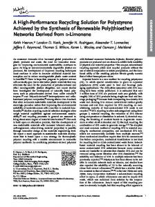
CHAPTER 1 INTRODUCTION Testing mixed-signal circuits, such as data converters, requires digital testing capabilities such as large pin count, edge accuracy and edge count, as well as analog testing capabilities such as low test system noise floor, analog signal bussing, synchronization, etc. [2]. Traditional analog and digital testers fall short of resources for testing the mixed-signal performance of data converters. Testers having mixed-signal resources (mixed-signal testers) are expensive [3]. Thus, testing cost is the biggest challenge that the next generation mixed-signal devices are facing [4]. This thesis focuses on reducing the overall cost for testing A/D converters. This chapter describes the basic concepts of A/D converter testing, the research work done in the past, the issues involved in testing of A/D converters, and the highlights the contribution of this thesis. Section 1.1 describes the major specifications for which A/D converters are tested. It also describes the standard testing procedures for A/D converters. Section 1.2 gives a brief account of the research work done in the past related to the A/D converter testing. Section 1.3 describes the testing issues for A/D converters and the proposed research. The major factors that impact the cost of testing A/D converters are highlighted in Section 1.4. The contribution of this thesis is highlighted in Section 1.5. 1.1 A/D Converter Testing A/D converter specifications can be classified as the static specifications and the dynamic specifications [5]. Given below are the specifications of A/D converters and the standard test procedures. 1
1.1.1 Static Specification Testing The specifications that are measured using a low-frequency test stimulus are called static specifications. The static specifications are differential non-linearity (DNL), integral non-linearity (INL), offset error, and gain error [6]. These specifications are a measure of an A/D converter’s non-linearity when the input signal has low frequency (near DC). DNL is the deviation of a code width from the ideal one least significant bit (LSB). The DNL of an A/D converter is shown in Figure 1. INL is the deviation of an A/D converter’s transfer function from the ideal transfer function as shown in Figure 2.
8 7 6 5
Code
4 3
DNL
2 1
1 LSB Analog Voltage
Figure 1. Differential non-linearity of an A/D converter.
N N-1
Ideal Transfer Function Code
INL
4 3 2
Actual Transfer Function
1
Analog Voltage
Figure 2. Integral non-linearity of an A/D converter. 2
6 5
Code
Offset Error
4 3 2 1
0.5 LSB
Analog Voltage
Figure 3. Offset error of an A/D converter.
N N-1
Ideal Transfer Function Code
4 3 2 1
Gain Error
Calibrated Actual Transfer Function Analog Voltage
Figure 4. Gain error of an A/D converter.
Offset error is the deviation of the first transition from the ideal one-half LSB value as shown in Figure 3. Gain error is the deviation from the ideal full scale value after the A/D converter transfer function is calibrated for offset error. It is shown in Figure 4. The histogram method is a standard method to measure the INL and DNL of an A/D converter as described in [7], [8]. It is also known as the code density test. The objective of the histogram test methodology is to measure the width of all the codes and calculate the DNL and INL specifications from the code width measurements. In this
3
OR
DUT
Test stimulus
INL/DNL
Output code histogram
Figure 5. Histogram testing.
method, a low-frequency test stimulus is applied to the A/D converter and a histogram of the output digital codes is obtained as shown in Figure 5. The histogram of the output codes shows the number of times each digital code word appears at the A/D converter output (number of hits). Generally, the test stimulus is a low frequency triangular ramp or a sinusoidal signal. Ideal output code histogram for a triangular ramp test stimulus is a flat distribution with equal hits per code. Ideal output code histogram for a sinusoidal test stimulus is a bathtub distribution. The deviation of the observed output code distribution from the ideal distribution is a measure of the non-linearity in the device. DNL of the A/D converter-under-test can be measured by counting the number of hits for each code and comparing them against the ideal number of hits for that code. There is no standard methodology to measure the offset and gain error. One of the testing methodologies is to measure the offset and the gain error from the line of best fit for the code transition points. 1.1.2 Dynamic Specification Testing Dynamic specifications are a measure of the high-frequency non-linear behavior of A/D converters [9]-[11]. Dynamic specifications are signal-to-noise ratio (SNR),
4
Frequency spectrum 20 0 -20 2nd Harm= -49dB
3rd Harm= -44.3dB
Power in dBm
-40 -60 -80 -100 -120 -140 -160
SNR=47.9dB, SFDR=60.3dB, THD=-36.6dB 0
0.5
1
1.5
2 2.5 3 Frequency in Hz
3.5
4
4.5
5 8
x 10
Figure 6. Frequency spectrum of an A/D converter.
spurious-free dynamic range (SFDR), total harmonic distortion (THD), second harmonic power and third harmonic power. A high-frequency sinusoidal test stimulus is applied to the A/D converter to measure the dynamic specifications. The A/D converter is clocked using a low-jitter clock and the frequency spectrum of output of the A/D converter-under-test is used to measure various dynamic specifications. It is shown in Figure 6. The frequency of the sinusoidal test stimulus is close to the A/D converter’s maximum rated input frequency. This is necessary to measure the worst-case nonlinearity specifications. The test stimulus frequency is chosen such that the coherent sampling condition, given in (1), is met. This is needed to prevent power leakage into the 5
adjacent frequency bins while constructing the frequency spectrum using a finite-point Fast Fourier Transform (FFT).
Fin Fsample
=
N window N record
(1)
where Fin is the input signal frequency, Fsample is the sampling clock frequency,
N window is an integer number of cycles within the sampling window, N record is the number of data points in the sampling window, and N record is a power of 2 to enable the use of a radix 2 FFT. N window and N record are relatively prime. Alternatively, if incoherent sampling is performed, a suitable windowing technique can be applied to the output signal to minimize the spectral leakage. 1.2 Previous Work Data converter testing is a very well researched topic. Research work includes modeling techniques, diagnosis, built-in-self-test techniques, statistical techniques etc. In this section, a brief account of the past research work is given. Techniques for modeling A/D converters were proposed in [12],[13]. The linear modeling of A/D converters was proposed in [14]-[18]. It is based on the concept that, there is a correlation between the code widths of an A/D converter. It models an A/D converter by a set of mutually independent and linear vectors. The number of vectors that are used to model an A/D converter is lesser than the number of codes. Thus, the static non-linearity testing of an A/D converter requires measurement of lesser number of 6
unknowns. It reduces the static non-linearity test time. Different diagnosis techniques are proposed in [19]-[21]. These techniques are architecture dependent and cannot be generalized across different architectures of A/D converters. IEEE guidelines for testing A/D converters are given in [22],[23]. It is evident from these guidelines that spectrally pure signals are needed for testing A/D converters. A method to generate spectrally pure signals for testing A/D converters is proposed in [24]. The authors use imprecise signals for testing A/D converters in [25],[26]. The use of wide bandwidth random noise (known as dither) to improve the SFDR and the harmonic performance of data converters is proposed in [27]. Strategies to test the performance of the A/D converters that are linearized with dither are proposed in [28],[29]. Built-in-self-test (BIST) is another approach that has been proposed for the static linearity testing of A/D converters [30]-[35]. BIST approach reduces the use of expensive test instrumentation but it requires integration of additional circuitry on the chip. Thus, silicon area overhead is a major issue in such an approach. Next, on-chip generation of precise test stimuli is an issue for BIST schemes. A methodology for generating precise, on-chip test stimuli is proposed in [36]. A technique for generating a precise source using imprecise on-chip sources is presented in [37]. Curve-fitting test methodologies to facilitate BIST are proposed in [38],[39]. Apart from these, many other test techniques have been proposed for A/D converter testing [40]-[42]. Still, there are several issues in A/D converter testing. They are explained in the next section.
7
24
In
S ig
g te ra
ma
tin
20
De
g
R
16
SA
lta
S
R
ub n ra
es 12
ng gi
ol
F la s h
8
uti
Class I
Class II
4
1gig
10M
100K
1K
10
Class III
Sampling Frequency
Figure 7. A/D converter classification.
1.3 Issues in A/D Converter Testing Although considerable research work is done on A/D converter testing, there are several issues that still exist. The testing issues for A/D converters are explained in this section. A/D converters are generally characterized by the resolution and the sampling speed. To cater to a wide variety of applications, the resolution of the A/D converters ranges from 8 to 24 bits and the sampling speed from 10 samples/second to 1 gigasamples/second (Gsps). Depending on the resolution and the sampling speed, there exist different A/D converter architectures as shown in Figure 7. Testing issues in A/D converters also depends on their resolution and the sampling speed. Based on the testing
8
issues, A/D converters can be broadly divided into three major classes as shown Figure 7. The testing issues for A/D converters are discussed in the following sub-sections. 1.3.1 Large Static Linearity Testing Time Static linearity testing time is large for A/D converters which have high resolution (12 bits or higher) and low sampling speed (5 Msps or lower). Such A/D converters are classified as Class 1 in Figure 7. They have a large number of codes that need to be measured during the static specification testing, and their sampling speed is low. Because of these characteristics, the static linearity test time is long, and it is a major issue for these A/D converters [43]. 1.3.2 Low-Jitter Clock Needed for Accurate SNR Measurement Measurement of accurate SNR of A/D converters having medium resolution (10 – 14 bits) and medium sampling speed (5 Msps – 250 Msps) requires a low-jitter clock. Such low-jitter clock sources are not available on low-cost test equipment. Hence, sampling clock jitter is a major problem for testing such converters Effect of different noise sources on the SNR measurement is described next in this section. The error introduced in an analog signal after it is quantized using a finite resolution A/D converter is shown in Figure 8. The quantization error for any AC signal, which spans more than a few LSBs, can be approximated by the saw tooth waveform. The RMS (root mean square) value of the quantization error can be obtained by using (2),(3). + LSB / 2
Quantization Noise =
1 ⋅ ∫ Q 2 ( t ) ⋅ dt LSB − LSB /2
9
(2)
Ideal ADC Transfer 4 3
Analog Signal
2 1
LSB
0 Q(t)
+1/2 LSB -1/2 LSB
LSB
2LSB
Quantization Error
Figure 8. Quantization error due to finite resolution of an A/D converter.
Quantization Noise(rms) =
LSB 12
(3)
Assuming a sinusoidal input signal whose amplitude is equal to the full-scale voltage of the converter, the signal-to-noise-ratio of the A/D converter having ideal transfer function can be given by (4)-(7). These equations assume that the only source of noise is the quantization error of the converter. Further, resolution of the A/D converter is assumed to be N. Full - scale Input v(t) =
LSB ⋅ 2 N ⋅ sin(2πft ) 2
RMS value of full - scale input v(t) =
10
LSB ⋅ 2 N 2 2
(4)
(5)
SNR = 20 log10 ⋅
rms value of input signal rms value of quantization noise
SNR = 20 log10 ⋅ 2 N + 20 log10 ⋅
3 2
(6)
(7)
SNR = 6.02 ⋅ N + 1.76dB
(8)
The SNR of an A/D converter as given by (8) assumes that there is no noise present in the test measurement system. Also, the noise due to jitter is assumed to be zero. Jitter in the sampling clock results in voltage error as shown in Figure 9. This error is given by (9). If a sinusoidal input signal is assumed, the voltage error depends on the frequency of the input signal, relative phase angle between the clock and timing jitter (10),(11). The root-mean-square error resulting from the timing jitter is given by (12).
∆v =
dv ⋅ ∆t dt
(9)
v( t ) = A sin( 2πωt + φ)
(10)
∆v = 2πAω cos( 2πωt + φ) ⋅ ∆t
(11)
2 2 Jitter Noise(rms) = 2πAω ⋅ (σ clk + σ int )
(12)
where σ clk is the root mean square value sampling clock jitter, and
σ int is the root mean square value of A/D converter internal jitter.
∆v
Voltage ∆t Jitter
Time
Figure 9. Error resulting from jitter.
11
Using (3) and (12), and assuming a full-scale sinusoidal input signal, SNR of an A/D converter measured using a test system is given by (13).
A2 SNR (dB) = 10 log( 2 2 2 2 ) 2 4π A ω (σ clk + σ int ) + Q 2 + Vn2
(13)
where, Q is the RMS value of quantization noise given by (3), and
Vn is the RMS value of noise present in the input signal. If it is assumed that the clock jitter is the only dominant source of noise present in the measurement, which is generally true for Class 2 A/D converters, (13) can be rewritten as (14). This equation establishes a upper-limit on the measurement of SNR in the presence of sampling clock jitter.
SNR (dB) = 10 log(
1 ) 2 4π ωin2 σ clk
(14)
2
20 non ideal ADC jitter rms 10ps 60M input SNR 48.43
0
-20
-40
-60
-80
-100
-120
0
1
2
3
4
5
6
7
8 7
x 10
Figure 10. Frequency spectrum shows SNR degradation resulting from clock jitter. 12
For example, if the test stimulus is a sinusoidal signal at 200 MHz and the sampling clock has RMS jitter equal to 2 ps, the upper limit on SNR that can be measured at the output, using (14), is equal to 52 dB. SNR for an N-bit ideal A/D converter is given by (8). Using (8), SNR of a 12-bit A/D converter (N=12) is equal to 74 dB. Thus, a sampling clock having an RMS jitter equal to 2 ps can not be used to measure the SNR performance of a 12-bit A/D converter. Clocks having lower jitter specifications are available but are very expensive to be used in production environment. Frequency spectrum of the output of a simulated 12-bit A/D converter is shown in Figure 10. The test stimulus is a sinusoidal signal having a frequency equal to 60 MHz. The RMS jitter in the sampling clock is equal to 10 ps. The SNR measured in this case was 48.43 dB as compared to the ideal SNR of 74 dB for a 12-bit A/D converter. Thus, jitter in the sampling clock is a major issue for testing such A/D converters. 1.3.3 High-Frequency Test Equipment Needed Dynamic testing of Class 3 A/D converters, which are characterized by low resolution (less than 10-bit) and high sampling speed (more than 200 Msps), requires a high-frequency sinusoidal test stimulus. Also, the digital capture frequency of the test instrumentation needs to be higher than the A/D converter-under-test to capture the digital output of the A/D converter-under-test. The testing issue for such A/D converters is generation and capture of high-frequency signals. High-cost test platforms having highbandwidth resources are needed to test such A/D converters. Apart from above, ground bounce noise is a testing issue for all classes of A/D converters. The presence of digital and analog signals on the same load board causes the noise resulting from the digital switching to affect the analog signals. Digital drivers in a 13
data converter, switch at the rate of the clock frequency. The return currents in the nonideal ground plane, generated by the switching of digital drivers, cause the ground voltage to fluctuate. This is referred as ground bounce. The noise resulting from the ground bounce is not a random noise. It depends on the number of digital drivers switching at a sampling instant. It also depends on the process parameters [44]. The ground bounce noise affects the analog input signal. Hence, there is a need to develop a test methodology to accurately estimate the data converter specifications in the presence of ground bounce. The test issues are summarized in Figure 11.
14
A/D Converters
Class I
Class II
Class III
Resolution more than 12 bits Frequency less than 5Msps
Resolution from 10 to 14 bits Frequency from 5 to 200Msps
Resolution less than 12 bits Frequency more than 200Msps
Noise resulting from ground bounce Large Test Time
Low-jitter clock needed
High-frequency test platform needed
HIGH TESTING COST Figure 11. Test problems for A/D converters.
15
1.4 Cost of Testing A/D Converters To develop a methodology for reducing the cost of testing A/D converters, it is necessary to understand different phases of production cycle of a semiconductor integrated-circuit (IC). In this section a brief overview of different phases of production cycle is given. Further, major elements that relate to the cost of testing an A/D converter are identified. Finally, the cost elements that are targeted in this thesis to reduce the cost of testing an A/D converter are described. Production cycle of an IC starts with a data sheet that is developed by the marketing and product engineers to target a specific customer, or based on broad market requirements. Based on the specifications that are included in the data sheet, a product characterization plan is developed by the test engineer. This plan is developed in consultation with the product and design engineers and it contains a list of all the tests that are performed on the device during the characterization phase. It also contains a list of the hardware resources that are needed to perform the tests listed in this plan. The goal here is to characterize the device in all possible test conditions to verify the design. Based on the characterization results the design is modified to meet the specifications listed on the data sheet. Conversely, data sheet can also be modified based on the characterization results. Characterization is done on a few devices and requires a few tester hours. Thus, test development engineers in this phase have access to high-performance testers. Based on the characterization results, a few critical tests are identified. These tests are listed on the production test list. During the production phase, high volume production of devices is done. The tests performed during the production testing are the critical tests that are identified during the characterization phase. Resulting from the high 16
volume production, the use of high-performance testers is not economically viable during this phase. The cost incurred in the characterization phase is a single time test development cost for a product. The cost is distributed over all the ICs that are manufactured. Thus, for the high volume products, per-IC characterization cost is very low. On the contrary, the production testing cost is fixed for an IC and does not decrease with the increase in number of ICs that are manufactured. Hence, it is economically viable to use highperformance testers in the characterization phase but not during the production testing. The production testing cost of a device depends on several parameters. A simplified model of the production testing cost is given by (15).
C p = C ts × Td
(15)
where Cp is the production test cost per device, Cts is the cost of test per second, and Td is the test time per device measured in seconds. In this equation the parameter, Cts (Cost of Test per second), depends on the tester depreciation, tester maintenance, tester idle time and other fixed costs like flooring cost. The tester depreciation is more for the expensive testers and thus this parameter is higher for the expensive testers. The parameter, Td (Test Time per device), depends on the number of tests in the critical test list, the duration of each test and test yield. These parameters are explained in detail further in this thesis. The main focus of this thesis is to use low-performance, low-cost testers and reduce the test time to reduce the overall production testing cost of A/D converters. 17
1.5 Contribution of This Thesis The aim of this thesis is to develop novel testing techniques for high-performance (high-resolution, high-speed) data converters, which are difficult as well as expensive to test using the state-of-the-art test systems. Following are the major contributions of the thesis.
•
Dynamic testing of high-speed A/D converters requires high-end testers. A test methodology that enables dynamic testing of such high-speed A/D converters using low-speed, low-cost testers is developed. The proposed technique can reduce the maximum required frequency capability of the tester by one-fourth resulting in significant tester cost savings.
•
Accurate measurement of SNR for high-performance A/D converters requires the use of a low-jitter clock source which is available only on high-cost test equipment. A test methodology that enables SNR measurement of high-performance A/D converters using a high-jitter clock sourced from a low-cost tester is developed in this thesis.
•
Measurement of static specifications (INL,DNL) incurs large testing time for A/D converters especially for high-resolution and low-speed converters. A selective code measurement methodology that exploits the knowledge of data converter architecture for test purposes is developed in this thesis. This reduces the testing time of such converter by 75%. A summary of the research work that was proposed is shown in Figure 12 on the
next page.
18
Figure 12. Summary of the research work.
19
CHAPTER 2 STATIC LINEARITY TESTING OF A/D CONVERTERS USING SELECTIVE CODE MEASUREMENT A novel methodology for testing the static linearity specifications of an A/D converter is described in this chapter. As explained in Section 1.1.1, the histogram method is used to measure the static specifications, such as, the integral non-linearity (INL) and the differential non-linearity (DNL) [7], of an A/D converter. In this method, a low frequency triangular ramp or a sinusoidal signal is used as a test stimulus. A histogram of the output of the A/D converter-under-test is obtained. The deviation of the observed histogram code distribution from the ideal distribution gives the DNL and INL of the A/D converter The inherent noise in an A/D converter and the measurement noise cause noise in the code transition edges. The histogram method averages out this edge noise to accurately measure the code widths by taking a large number of samples. Once the code widths are measured, the DNL and INL can be calculated by using (16) and (17). DNL = M − 1 i i j= i
INL i = ∑ DNL j
0 < i < 2N − 1
(16)
0 < i < 2N −1
(17)
j=1
where Mi is the code width for code i, and N is the A/D converter resolution. The number of samples that are required for the histogram testing depends on the resolution of the A/D converter and the level of accuracy desired in the DNL 20
measurement. As the resolution of the A/D converter increases, the number of samples required to achieve the desired accuracy in the code width measurement increases by a factor of two for each bit added to the converter’s resolution. This results in a large test time for measuring all the code widths to calculate the INL and DNL specifications. Although, large test time for the static linearity testing of A/D converters is an issue for all classes of A/D converters, it is a major problem for Class 1 A/D converters. This is resulting from the low data sampling rate and the high resolution of these devices. For example, the test time for INL and DNL specification testing of a 12-bit successive approximation register (SAR) A/D converter using the conventional histogram method can be as high as 40% of the total A/D converter test time. In this chapter, a novel test methodology to measure the INL and DNL specifications of A/D converters is described. The developed test methodology is based on the fact that, the non-idealities in the code widths of an A/D converter are correlated to, and are dominated by the manufacturing variations in the specific components present in the A/D converter. Therefore, by measuring a subset of total code widths that are directly affected by the manufacturing variations in these components, all the code widths can be estimated accurately. The proposed methodology identifies specific codes that are directly affected by the deviation in the A/D converter component’s values resulting from manufacturing variations. A piecewise linear test stimulus is then generated to measure these specific code widths. The test methodology was verified on a SAR and a pipelined A/D converter. The key contributions of the developed test methodology are as follows: •
It reduces the linearity test time of A/D converters by estimating the INL and DNL from the measurement of a subset of the total code widths.
21
•
No additional hardware is required to implement the proposed methodology.
•
It uses a specially crafted piecewise-linear ramp to accurately measure the relevant code widths. The rest of the chapter is organized as follows. Previous research work related to
the static linearity testing of A/D converters is highlighted in Section 2.1. The developed test methodology is explained in Section 2.2. Its implementation on different test cases is explained in Section 2.3.
The economic impact of the developed methodology is
highlighted in Section 2.4. 2.1 Previous Work Linearity testing of A/D converters is a widely researched topic. Generation of precise test signals and reduction of test time has been the primary focus of the past research on this topic. The issues with histogram testing are discussed in [45]-[49]. The authors present a statistical technique for characterizing an A/D converter using Gaussian noise as the test stimulus for the histogram test set-up in [50]. However, the results show a significant error in the measurement of maximum INL. Also, the number of samples needed for the test procedure is large. A different methodology that uses noise as the test stimulus is presented in [51]. Testing of A/D converters based on a linear model has been proposed in [15][18]. These test methodologies exploit correlations between the widths of different codes of an A/D converter. A linear model that relates all the code transition edges to a few set of independent parameters is constructed through a set of statistical measurements across a large number of devices. The number of parameters used to model an A/D converter is 22
significantly smaller than the number of converter output codes. Thus, the static nonlinearity testing of an A/D converter requires measurement of fewer unknowns and the test time is significantly reduced. However, these methods need initial development of models and recalibration of models when the process shift occurs. The past research has also focused on INL estimation using frequency domain methods [52]-[54]. In [53], the authors filter noise from the output frequency spectrum of an A/D converter and perform the inverse FFT of this signal to reconstruct the input signal. This reconstructed signal is then compared against the original input signal to measure the INL. In [54], the A/D converter transfer function is approximated by a polynomial and the INL is estimated from the FFT spectrum. Frequency domain methods reduce test time significantly but they are inaccurate for measurement of specifications such as maximum INL and DNL [53], [54]. Several built-in-self-test (BIST) techniques have been proposed to measure the static specifications of A/D converters [30]-[35]. However, such techniques incur cost in terms of added silicon area for the on-chip test circuitry. A methodology for testing the INL and DNL specifications of data converters using nonlinear test stimulus is proposed in [26]. In [55], the authors describe a design-for-testability (DFT) methodology to decrease the static linearity test time of SAR A/D converters by reducing the SAR algorithm of the converter. This results in the test time reduction, when compared to the servo loop method of determining the code edges. Other methods such as oscillation based testing [56] have also been proposed. The methods described above do not exploit the circuit topology of the converter for test time reduction. In this research, a new test methodology for INL and DNL testing
23
of A/D converters is developed. This methodology is based on the architecture of A/D converters. The proposed methodology measures the converter specifications as accurately as the histogram methodology, and reduces test time by one-fourth. 2.2 Proposed Methodology Architecture of an A/D converter depends on its resolution and sampling speed. In this work, A/D converters are represented with a generic architecture as shown in Figure 13. The A/D converter shown in the figure is divided into multiple stages. Each stage is a low-resolution, ‘flash-type’ A/D converter having a resolution Ri (where, ‘i’ is the stage number). In general, there is additional inter-stage circuitry that is not shown in the figure. An extreme case of this generic architecture is a flash A/D converter where the number of stages is one and all the bits are contributed by that stage. The other extreme case is an N stage, N-bit pipelined A/D converter where each stage contributes one bit to the output word.
Stage 2
Stage 1 I/P
R1 +
R2
Stage N +
RN
O/P
R = R1 + R2 +…….RN
Figure 13. Generic A/D converter architecture.
Stage 1
Stage 2
Stage N
b1 b2… bR1 | b(R1+1) … b(R1+R2) | … |b(R1+…R(N-1)+1)… b(R1+…RN) Figure 14. Digital output of the A/D converter. 24
Total resolution of the A/D converter (number of bits) is the sum of the resolution of all its stages. Each stage contributes a fixed number of bits, equal to its resolution, to the output. Further, it is assumed that the first stage is the most significant stage (i.e. it contributes the most significant bits) and the last stage is the least significant stage (i.e. it contributes the least significant bits) as shown in Figure 14. In this figure bi represents ith bit and Ri represents number of bits contributed by ith stage. 2.2.1 The Concept of Selective Code Measurement The proposed test methodology is based on the fact that code width variations result primarily from manufacturing variations in the value of components from their nominal value in each stage of an A/D converter. Since each stage computes only a subset of the total number of bits generated by the converter, the non-idealities in the value of components of a stage impact specific codes. Further, the codes that are affected by a particular stage can be divided into sets, such that, each set of codes is affected in a similar way. Thus, if the DNL of one such set of codes is measured, the DNL of all the other sets of codes that are affected by that particular stage can be determined. The performance of an A/D converter for all the output codes can then be determined by measuring one such set of codes for every stage. Once the DNL of all the codes is obtained using the proposed methodology, the transfer function of the A/D converter is obtained by summing the respective code widths. The INL values for each code can be computed by comparing the obtained transfer function from the ideal A/D converter transfer function.
25
To explain the identification of sets of codes that have similar DNL values, a 4-bit A/D converter example is shown in Figure 15 . The A/D converter in this example consists of two stages, each contributing 2 bits to the output of the A/D converter. In this example, width of codes {0, 1, 2} corresponds to Set 1, {4, 5, 6} corresponds to Set 2, {8, 9, 10} corresponds to Set 3 and {12, 13, 14} corresponds to Set 4. For the codes present in Set 1 the logic state of bits contributed by Stage 1 remains the same (‘00’). Similarly for Set 2, 3 and 4 the logic state of bits contributed by Stage 1 remains the same (‘01’ , ‘10’ and ‘11’ respectively). It is observed that the code transitions within a set occur only resulting from the change of logic state of bits in Stage
Stage 1
Stage 2
Code: 0 Code: 1 Code: 2 Code: 3
0 0 0 0
0 0 0 0
0 0 1 1
0 1 0 1
Code: 4 Code: 5 Code: 6 Code: 7
0 0 0 0
1 1 1 1
0 0 1 1
0 1 0 1
Code: 8 Code: 9 Code: 10 Code: 11
1 1 1 1
0 0 0 0
0 0 1 1
0 1 0 1
Code: 12 Code: 13 Code: 14 Code: 15
1 1 1 1
1 1 1 1
0 0 1 1
0 1 0 1
Set 1
Set 2
Set 3
Set 4
Figure 15. 4-bit, 2-stage pipelined A/D converter.
26
2. Hence, the DNL of the codes present in these four sets occur only resulting from the non-ideal components present in Stage 2. Also, the non-ideality in the code widths (DNL) of all the four sets is equal as it is caused by the same underlying electronics components (Stage 2). Thus, if the DNL of one of the four set of codes is measured, the DNL of the other three set of codes can be directly calculated from the measurements. In this example, the code widths that need to be measured for the A/D converter static characterization are {0, 1, 2, 3, 7, 11 and 15}. As the DNL of the codes present in Set 2, 3 and 4 is equal to that of Set 1, only code widths of Set 1 are measured. The A/D converter transfer function can be constructed by adding the measured code widths. Generalization for a multistage A/D converter is shown in Figure 16. In this example, A/D converter has N stages and Stage N contributes RN least significant bits. The codes transitions that occur resulting from the change of logic state of these RN bits (logic state of all the higher order bits remains unchanged) are governed only by the components of Stage N. Hence, the non-ideality in the width of such codes is only resulting from the non-ideal components used in Stage N. Codes that are affected by Stage N are divided in different sets as shown in Figure 16. Set 1 corresponds to the codes from 0 to (x-2), and Set 2 corresponds to the codes from x to (2x-1). Similar sets can be obtained by varying the logic state of the ‘more significant bits’. The widths of all the codes present in these sets are governed by the components in Stage N. If the code widths (or DNL) of one set is measured, the code widths of similar sets can be computed. Same concept can be extended to other stages and one set of codes for each stage is measured. Thus, by measuring specific code widths, transfer function of the A/D converter can be obtained.
27
More Significant Stages
Code: 0
Code: x-2 Code: x-1 Code: x
Code: 2x-1 Code: 2x
Stage N
00…00 0…00 00…00 0…01 ……………..……… 00…00 1…10 00…00 1…11 00…01 0…00 00…01 0…01 ……………..……… 00…01 1…10 00…01 1…11
Set1
Set2
x = 2R N
Figure 16. Identification of similar set of codes for stage N.
2.2.2 Reduction in Test Time As illustrated in the previous section, to measure the non-ideal effect of the components in Stage N, it is necessary to measure the width of 2RN output codes. The total number of code widths (or DNL) that need to be measured for estimating the nonideality of all the components in an A/D converter is given by (18). This is significantly less than the number of code widths that need to be measured if the histogram method is used to measure the INL and DNL of an A/D converter (19).
CW
sel = 2
CW hist
R1
= 2
+ 2
R2
+ ... 2
R 1 + R 2 + ... R N
where Ri is the resolution of ith stage.
28
RN
(18) (19)
An algorithm for identifying the codes that need to be measured to capture the effect of non-ideal components in all the stages of an A/D converter on its output code widths is described in the following section. 2.2.3 Generation of Test Stimulus For generating the test stimulus, the codes that need to be measured are identified first. Next, a piecewise linear ramp is programmed such that its slope is low (slow ramp) when it crosses over the codes whose widths are to be measured and its slope is high (fast ramp) when it crosses over all other codes. The algorithm for identification of codes and generation of test stimulus is shown in Figure 17. The non-linearity in the A/D transfer function may displace the codes from their ideal position. To ensure that the slow ramp measures the desired code, the length (time duration) of the each slow section of the ramp is at 7 least significant bits (LSBs). The desired slope for the fast ramp is infinite (the most aggressive ramp that can be applied by the test system is used). 2.2.4. Calibration The proposed method is based on the concept that the DNL (or code width) of different set of codes is equal because it is caused by non-idealities in the same components. Thus, the DNL of a few codes is measured, and the DNL (or the code width) of rest of the codes is estimated from them. The transfer function is then obtained by adding the code widths cumulatively. Resulting from the inherent noise in an A/D converter, and the external noise in the measurement system, edge noise appears near code transitions.
29
Piecewise Linear Ramp Generation Algorithm N = Number of stages of the converter. Ri = Number of bits corresponding to Stage i. H= Desired number of hits/code for selected codes LSB = Value of a least significant bit.
Input: (N, Ri,H,LSB) 1 Choose the least significant stage. 2 While the chosen stage is not the most significant stage. 3 Search for the codes C such that for transition from C to C+1, only the bits that are contributed by the chosen stage change logic state AND all the bits of the stages more significant than the chosen stage have logic state ‘0’. 4 Add C to the list L. 5 Choose the next more significant stage. 6 End while. 7 Search for codes C such that for the transition from C to C+1, only the bits that are contributed by the chosen stage change the logic state. 8 Add C to the list L. 9 Program a piecewise linear ramp from (L-3)*LSB to (L+4)*LSB for all the codes in the list L having a slope adjusted to obtain the specified number of hits per code. Output:(Piecewise linear ramp test stimulus).
Figure 17. Piecewise linear ramp generation algorithm.
30
This noise can be as high as 200m LSB, and it causes error in the measurement of the widths of the desired codes. The error in measurement of these code widths is small (20-30milliLSB). But, when these code widths are added to obtain the overall A/D converter transfer function, the error adds up cumulatively and results in a deviation of the transfer function from the actual transfer function. To eliminate this inaccuracy in measurement resulting from edge noise, calibration is necessary. In this process, the estimated transfer function is calibrated such that the cumulative error is eliminated The last slow ramp section of the test stimulus is used for calibration. This is shown in Figure 18. The output of the A/D converter for this section determines the code position of the A/D converter at the applied voltage. For this code position, the
Figure 18. An example of piecewise linear test stimulus. 31
estimated transfer function gives the estimated voltage. The difference between the applied voltage and the estimated voltage gives the voltage error at that code position. The estimated transfer function is then corrected for the error by linearly scaling the observed voltage error to give a calibrated transfer function (TFcal). Let the last slow ramp section of the test stimulus have the following characteristics. Starting voltage is Vi and the slope is M hits/code. Let the lowest output code of the converter corresponding to this section be code ‘x’, and number of hits on this code be P. The actual transfer function (TFact) at code ‘x’ is given by (20). TFest is the estimated transfer function. VE(x) is the voltage error in the estimated transfer function at the code ‘x’ and is given by (21). The calibrated transfer function TFcal is given by (22), where N is the resolution of the A/D converter.
P TFact(x) = Vi − (1− ) ⋅ lsb M
(20)
VE ( x ) = TFact ( x ) − TFest ( x )
(21)
TFcal(i) = TFest (i) +
i ⋅ VE(x) x
0 ≤ i ≤ 2N
(22)
2.3 Implementation of the Proposed Methodology The proposed test methodology was implemented on two different types of A/D converter architectures using software simulations. The test methodology was also implemented on a commercially available A/D converter using hardware experiments. These three case studies are described next.
32
4 bits
8 bits
Stage 1
Stage 2
+
S/H In
A
+
Out
-
A/D
D/A
Figure 19. Simulated pipelined A/D converter architecture model.
2.3.1 Case Study I: Implementation on a Simulated Pipelined A/D Converter In the first case study, a two-stage, 12-bit, 80 Msps, pipelined A/D converter was used as a test vehicle. A behavioral level model of the A/D converter was made and the simulations were performed using MATLAB. 2.3.1.1 Pipelined A/D Converter Architecture The architecture of the simulated pipelined A/D converter is shown in Figure 19. The first stage was simulated as a 4-bit ‘flash-type’ A/D converter and the second stage as an 8-bit ‘flash-type’ A/D converter. Ideally, in an A/D converter transfer function all the codes have equal width. Resulting from the manufacturing variations, the code widths deviate from their ideal value of one LSB. This introduces non-linearity in the A/D converter transfer function. This non-linearity is resulting from the manufacturing variations and was introduced in the simulated model by varying the code widths from their ideal one LSB value. ‘Flash-type’ A/D converters of both the stages were modeled by a ‘random transfer function’ model. The random transfer function model is obtained by varying the
33
code widths randomly from their ideal value to introduce non-linearity. The non-linearity in the width of a code has no correlation to the non-linearity in the width of any other code in a ‘flash-type’ A/D converter. (Detailed ‘flash-type’ A/D converter architecture is given in Appendix A). Thus, random code width variation is a valid technique to obtain the transfer function of a Flash A/D converter. In this research work, the code widths were varied from their ideal value of 1 LSB by using a Gaussian distribution having a standard deviation equal to 0.2 LSB and mean equal to zero. Resulting from the thermal noise of the components and the noise resulting from active devices, the code transition points are not fixed. A noise known as code edge noise appears at the code transition points and causes them to vary from one sampling instant to another. To account for this real device behavior, code edge noise was added to the code transition points in the behavioral model of Flash A/D converter. The code edge noise that was added was random noise having a uniform distribution with maximum value equal to 0.2 LSB (volts). Development of the ‘flash-type' A/D converter behavioral model is shown in Figure 20.
1LSB ± ∆
1LSB ± ∆
X
X
X
1LSB
X
X
X
Non-linear Transfer Function
X-1
Ideal Transfer Function
Code
X-1
X-1
Code
Noise on Non-linear Transfer Function with Code Edge Noise
Figure 20. Behavioral model development of a Flash A/D converter.
34
Figure 21. INL of a simulated pipelined A/D converter instance.
The pipelined A/D converter that was simulated was a two-stage A/D converter with each stage having a ‘flash-type’ A/D converter. After simulating each stage, the full A/D converter transfer function was obtained. INL plot of a simulated pipelined A/D converter instance is shown in Figure 21. 2.3.1.2 Selective Code Measurement The codes that need to be measured were determined using the piecewise linear ramp generation algorithm given in Section 2.2.3. The code widths that were measured are given by (23).
Codes ∈{[0 254], 255 + 256 ⋅ i}
35
0 ≤ i ≤ 254
(23)
A piecewise linear ramp was generated to measure these codes. The slope of the slow part of the ramp was set such that the number of hits per code was 64. The slope of the fast part of the ramp was infinitely large (DC offset was added). The transfer function of the A/D converter was obtained from the measured code widths. The calibration of the estimated transfer function was performed as explained in Section 2.2.4. 2.3.1.3 Simulation Results Fifty simulation instances of pipelined A/D converter were generated. The total number of samples required by the proposed methodology was 22,158. The specifications calculated were maximum (+/-ve) INL. A comparison of the calculated specifications and the actual specifications is shown in Figure 22. The specifications of the same simulated A/D converter instances were measured using the histogram method. A linear ramp having a slope such that, the number of hits per code was 64, was used in this method. The total number of samples required by the
Figure 22. Actual and estimated maximum (+/-ve) INL. 36
histogram method was 262,144. A comparison of error in estimation of the specifications using the histogram method and the proposed method from the actual specifications is given in Table 1. It shows that the proposed method produces results that are as accurate as the results obtained using the histogram method for maximum (+/-ve) INL. The number of samples required by the proposed methodology is 10 times lesser than the number of samples required by the histogram methodology. 2.3.2 Case Study II: Implementation on a Simulated SAR A/D Converter In this case study, a 12-bit, 500Ksps Successive-Approximation-Register (SAR) A/D converter was used as a test vehicle. The A/D converter was modeled using a behavioral modeling technique in MATLAB. The test set-up was also simulated in MATLAB. 2.3.2.1 SAR A/D Converter Architecture Unlike the pipelined architecture, the output bits are estimated serially in SAR architecture [57]. The SAR control logic sets the bits of D/A converter using a binary search algorithm. Its objective is to set the bits of D/A converter such that the output of
TABLE 1 Comparison of Error in Estimation of Specifications for Case Study I Histogram Method
Selective Code Measurement Method
96.0 33.3
87.8 29.0
82.2 19.9
87.0 28.8
+ve INL
Max. error Mean error -ve INL
Max. error Mean error All values are in milliLSB.
37
the D/A converter is as close to the input signal as possible. D/A converter forms a major part of the SAR A/D converter as shown in Figure 23. The D/A converter simulated in this research work consist of an array of weighted capacitors. The values of the capacitors in the D/A converter were randomly perturbed to generate different simulation instances of A/D converter. The random perturbation had Gaussian distribution. The mean of the distribution was zero and the standard deviation was 2% of the nominal value. The transfer function of the A/D converter was obtained based on the D/A converter capacitor values. To simulate the real device behavior, code edge noise was added to the code transitions. The code edge noise was random noise having a uniform distribution with maximum value equal to 0.2 LSB (volts). INL plot of a simulated A/D converter instance is shown in Figure 24. 2.3.2.2 Selective Code Measurement The codes that need to be measured were determined using the piecewise linear ramp generation algorithm given in Section 2.2.3. The code widths that were measured are given by (24).
Codes ∈{ (2i - 1)}
0 ≤ i ≤ 11
(24)
A piecewise linear ramp was then generated to measure these codes. The slope of the slow part of the ramp was set such that the number of hits per code was 512. The slope of the fast part of the ramp was infinitely large (DC offset was added). The transfer function of the A/D converter was obtained from the measured code widths. The calibration of the estimated transfer function was done as explained in Section 2.2.4.
38
Digital O/P
I/P
Sample and Hold
Comparator SAR D/A Converter Control Logic Analog Output
2N C
MSB
2C
C
C
LSB
Vref
Ground
Figure 23. Successive Approximation Register architecture.
Figure 24. INL plot of a simulated SAR A/D converter instance.
39
2.3.2.3 Simulation Results Ninety instances of the simulated A/D converter were generated. The total number of samples required by the proposed methodology was 34,816. The specifications measured were maximum (+/-ve) INL. The histogram method was used to measure the specification of the same simulated A/D converter instances using a linear ramp. The slope of the ramp was set such that number of hits per code was 64. The total number of samples taken using the histogram method was 262,144. A comparison of error in estimation of the specifications using the histogram method and the proposed method from the actual specifications is given in Table II. The total number of samples used by the proposed methodology was significantly lesser than the number of samples used by the histogram method.
TABLE II Comparison of Error in Estimation of Specifications for Case Study II Histogram Method
Selective Code Measurement Method
119.0 42.1
45.5 13.9
117.4 65.2
92.3 16.5
+ve INL
Max. error Mean error -ve INL
Max. error Mean error All values are in milliLSB.
40
2.3.3 Case Study III: Hardware Implementation on a SAR A/D Converter A commercially available 12-bit, 500Ksps SAR A/D converter was used as a test vehicle for this case study [58]. The test platform was A580 tester from Teradyne. 2.3.3.1 Selective Code Measurement The codes measured in this case study were same as the codes measured in Case Study II because the specifications (resolution and architecture) of A/D converter-undertest are the same. Precision-low-frequency-source (plfsrc) housed in the tester was used to generate the piecewise linear ramp. The slope of the slow part of the ramp was set such that the number of hits per code was 256. The slope of the fast part of the ramp was set such that the number of hits per code was 0.5. The slope of the fast ramp was adjusted to minimize ringing and overshoot of the test stimulus. The ringing and overshoot occur resulting from the filter characteristics of the precision-low-frequency-source (plfsrc). The transfer function of the A/D converter-under-test was obtained from the measured code widths. The calibration of the estimated transfer function was performed as explained in Section 2.2.4. 2.3.3.2 Hardware Results The proposed methodology was used to measure the maximum (+/-ve) INL and DNL of five A/D converter devices. The total number of samples required by the proposed methodology for each device was 17,886. The histogram method was used to estimate the specifications of the same devices using a sinusoidal signal. The total number of samples required by the histogram method was 262,144. INL plots of one of the A/D converters measured using the histogram method and the proposed method are shown in Figure 25 and Figure 26. The experiments show that the proposed methodology 41
Figure 25. INL plot measured using the histogram method.
Figure 26. INL plot measured using the proposed method.
42
measured the INL and DNL of the A/D converter devices very accurately. Table III shows the value of the specifications obtained by both the methods for different devices. Column 3 in the table shows the deviation in the results obtained using the proposed methodology from the results obtained using the histogram methodology.
TABLE III Measured Value of Specifications using Both Methods Case Study III Selective Code Deviation from Histogram Histogram Measurement Method Method Method +ve INL
Device 1 Device 2 Device 3 Device 4 Device 5
419.6 463.0 405.8 399.8 407.0
446.2 430.6 454.4 434.4 382.2
-26.8 33.6 -48.6 -34.6 24.8
-431.4 -432.4 -385.4 -387.6 -346.6
-436.2 -448.0 -482.4 -470.0 -420.2
4.8 15.6 97.0 82.4 73.6
545.0 558.0 585.2 540.2 557.8
529.8 549.2 543.0 542.2 528.8
15.2 8.8 42.2 -2.2 29.0
-289.6 -289.2 -301.4 -273.2 -288.0
-213.2 -253.0 -257.2 -250.6 -246.0
-76.4 -36.2 -44.2 -22.6 -42
-ve INL
Device 1 Device 2 Device 3 Device 4 Device 5 +ve DNL
Device 1 Device 2 Device 3 Device 4 Device 5 -ve DNL
Device 1 Device 2 Device 3 Device 4 Device 5
Test time for histogram method was 1.22 sec/device. Test time for the proposed method was 0.28 sec/device. 76% of test time reduction was achieved. All values are in milliLSB.
43
TABLE IV Repeatability Analysis of Histogram Method Case Study III Maximum Deviation for Five Runs +ve INL 63
-ve INL 76
+ve DNL 82
-ve DNL 77
All values are in milliLSB.
The repeatability analysis of the histogram method was done to obtain the error margin from run-to-run. This was done by repeating measurements five times on all the devices. The maximum deviation in the values of the specifications is shown in Table IV. Comparing these values to the deviation in specifications measured using two methods (shown in Table III column 3), it can be concluded that the proposed method estimates the specifications which are within the histogram method repeatability limits. The test time to measure the specifications of one A/D converter using the proposed method was 0.28 sec. as compared to 1.22 sec using the histogram method. 2.4 Test Cost Analysis As explained in Section 1.4, the production testing cost of an IC depends directly on the test time. The parameter, Td (Test Time per device), given in (15) is not straightforward and depends on many parameters. It depends on total number of tests that are performed during production testing and the duration of each test. It also depends on the ratio of good ICs to the total number of ICs tested (test yield).
Td ( Test Time per device) =
∑ T(i) ×
i∈all the tests
where T(i) is the test time for test i. and 44
Total no. of ICs Tested Total no. of good ICs
(25)
i denotes the list of all the production tests. However, assuming the test yield remains the same, reduction in the duration of a test directly reduces Td and hence Cp (production test cost per device) as given by (15) and (25). The annual savings for a semiconductor company based on the number of devices manufactured annually are shown in Table V. It shows the savings based on three different categories of testers. The cost of test per second for different type of testers was obtained from a semiconductor manufacturing vendor that operates these testers in production environment. The savings shown in Table V are for one product assuming a production rate of 1 million devices per year. The economic analysis shows that significant savings can be achieved by implementing the proposed methodology for linearity testing of A/D converters. The implementation of the proposed methodology does not require any modifications to the load board. The proposed methodology can be implemented by making necessary changes in the test routines. Thus, it is possible to implement the proposed methodology on devices that are already in production.
TABLE V Economic impact of the proposed methodology. For hypothetical production of 1,000,000 devices/yr. Tester Type Low-end Middle-end High-end
Cost/sec. 0.8 cents 4.3 cents 6.4 cents
Test Time Reduction 0.94sec/device 0.94sec/device 0.94sec/device
45
Yearly Savings $7,520 $40,420 $60,160
CHAPTER 3 DYNAMIC SPECIFICATION TESTING OF HIGH-SPEED A/D CONVERTERS USING LOW-COST TEST INSTRUMENTATION
As described in the last chapter, test time directly adds to the cost of an A/D converter. The conventional tests that are used to measure the static specifications take a long time and hence, there is a need to develop a testing methodology that reduces the static linearity test time. One such testing methodology was developed and described in the last chapter. However, the tests that measure the dynamic specifications of an A/D converter require lesser number of samples and hence, the test time is short. The bottleneck for such tests is the use of high-bandwidth test equipment, the cost of which is very high. As explained in Section 1.3, testing of high-speed A/D converters require highbandwidth test equipment. In this chapter, a methodology for testing high-speed A/D converters using low-bandwidth resources is described. The proposed test methodology is based on the alternate testing approach. The key contribution of the developed test methodology is the following: •
It enables dynamic specification testing of an A/D converter using test instrumentation that is running at a lower frequency than the A/D converter-undertest. The rest of the chapter is organized as follows. Section 3.1 gives an overview of
the alternate testing. The proposed low-cost test strategy is described in Section 3.2. Section 3.3 describes the simulation of the proposed approach. The hardware validation
46
results are presented in Section 3.4. The cost impact of the proposed methodology is shown in Section 3.5. 3.1 Overview of Alternate Testing The alternate test methodology was developed by Variyam and Chatterjee [59]. Alternate test methodology is based on the concept that, because of manufacturing variations, the specifications of a device-under-test (DUT) vary in a correlated manner with the measurements made on it, when an appropriate test stimulus is applied to the DUT. If such a correlation exists between the specifications and the measurements, a variation in the process parameters causes variation in specifications of a device as well as a corresponding variation in the measurements made on that device in presence of an appropriate test stimulus, henceforth called alternate test stimulus. Thus, instead of performing the conventional tests on a DUT, it is possible to excite the DUT using the alternate test stimulus and use the measurements to calculate the specifications of the DUT. The term, ‘measurements,’ refer to time domain samples or frequency domain information of the output waveform of the DUT in the presence of a test stimulus. To calculate the specifications of a device from the measurements made in the presence of an alternate test stimulus, the functions that map the measurement space to the specification space, are need to be known. These mapping functions are also called models. To generate these models, a set of devices is chosen and the conventional tests are used to obtain their specifications. The same set of devices is excited with the alternate test stimulus and the measurements made on these devices are stored. Nonlinear regression techniques are then used to generate the models that map the
47
measurements made on the devices to the specifications of the devices. The alternate test overview is shown in Figure 27. Once the models are developed using a set of few devices, the specifications of other devices are estimated by exciting the DUT using the alternate test stimulus and capturing the measurements. These measurements are used with the models to calculate the specifications of the DUT. There is a need though, to generate a specially crafted test stimulus such that maximum correlation between specifications of the device and the measurements is observed. The generation of alternate test stimulus is test case specific and varies from application-to-application. Alternate testing methodology has been applied to analog and RF devices with the goal of test time reduction [60]-[62]. The authors achieve test time reduction by generating alternate tests which are shorter in duration than the conventional tests. It is also possible to obtain multiple specifications of
Alternate Test Stimulus
Models
m1
m2
m3
S2
Device-under-test
Measurement Space S1
Specification Space
Before perturbation Manufacturing Perturbations
Figure 27. Alternate test overview.
48
After perturbation
a device using a single alternate test, instead of multiple conventional tests, thus saving test time. In this research work, the alternate testing methodology is applied to ease the tester resource requirement, instead of test time reduction for which the alternate testing is conventionally used. 3.2 Proposed Low-Cost Test Strategy In this section, the test methodology that is developed to measure the dynamic specifications of high-speed A/D converters using low-bandwidth test instrumentation is illustrated. The proposed approach is based on the alternate testing concept and is divided in two phases as explained below. Model Building Phase: This is the test generation phase. The objective of this phase is to develop correlation models that can be used later in the testing phase. In this phase, the conventional dynamic testing methodology (explained in Section 1.1) is used to obtain the specifications of a set of A/D converters using a high-performance tester. Highperformance tester here refers to a tester that has resources, namely data acquisition system, which runs at a frequency higher than the sampling frequency of device-undertest. Thus, it is implied that the tester resources have higher bandwidth than the deviceunder-test. The set of A/D converters that are used in this phase are preferably selected from different production lots so that they are a good representation of the process parameter space. The same set of A/D converters is then excited with an alternate test stimulus. The alternate test stimulus is generated using a low-performance tester as shown in Figure 28. The low-performance tester has resources running at a frequency lower than the sampling
49
Low Performance Tester
Mixer
BPF
LF LO
Multi-Tone Stimulus
DUT Input
Clk
External Clock 0
Output
Output
Cable for Synchronization
Figure 28. Single-mixer low-cost test set-up.
frequency of the device-under-test. The alternate test generation procedure is further described in Section 3.2.1. Response of the A/D converters to the alternate test stimulus is under-sampled by the tester and stored. Multivariate Adaptive Regression Splines (MARS) regression technique is then used to develop the mapping functions (models) between the response of the A/D converters and their specifications. MARS is explained in Section 3.2.2. Testing Phase: This phase is implemented in the production environment to test the dynamic specifications of A/D converters. In this phase, A/D converters are tested using the low-cost test set-up shown in Figure 28. Their specifications are estimated by obtaining their responses to the alternate test stimulus and using the mapping functions that were developed in the Model Building Phase. The alternate test generation procedure is explained next.
50
3.2.1 Alternate Test Stimulus Generation The dynamic performance of an A/D converter decreases with the increase in input frequency. This occurs resulting from the increased parasitic affects at higher frequency of operation for transistors. To measure the worst-case specifications of an A/D converter, it is generally tested at its maximum rated input frequency. The conventional method uses a single tone, spectrally pure, low-noise, sinusoidal signal at the maximum rated frequency of an A/D converter to test the dynamic specifications. The dynamic specifications can be directly measured by observing the frequency spectrum of the output of A/D converter. It is imperative to excite the high-frequency non-linear affects of an A/D converter in any dynamic testing methodology to test it for worst-case scenario. The proposed approach uses an up-conversion mixer to generate a high-frequency sinusoidal tone from the low-frequency source available on a low-cost tester. In general, any other component such as a frequency-doubler can be used to generate high-frequency sinusoidal tone from the low-frequency source available on a low-cost tester. In the proposed approach, the low-frequency signal from the tester (LF) is mixed with a localoscillator (LO) signal by the mixer as shown in Figure 28. Local-oscillator signal is also generated using the low-cost tester. A mixer is a non-linear device and hence it generates sinusoidal tones at several frequencies. The frequency tone at which the dynamic specifications of an A/D converter need to be measured is referred as ‘testing frequency’. All the other frequency tones are referred as un-wanted tones. The output of the mixer is shown in Figure 29. A band-pass filter is used to filter most of the un-wanted tones. The use of filter decreases the power
51
Un-wanted frequency tones
Testing Frequency
Figure 29. Alternate test stimulus at the output of the mixer.
of the un-wanted frequency tones. However, the test stimulus is not as spectrally pure as the test stimulus that is used in the conventional method of testing. The frequency of the LF and LO tones is adjusted in such a way that the frequency of the up-converted tone is equal to the testing frequency. The relation between different frequency tones is shown in (26). ωIN = ωLF + ωLO where ω LF is the frequency of the LF signal,
ω LO is the frequency of the LO signal, and 52
(26)
Mixer IF
Low Performance Tester
BPF LO
Multi-tone Test Stimulus
External Clock
DUT Input Output
1
0
Clk
2
BNC Cable for Synchronization
Figure 30. Two-mixer test set-up.
ω IN is the testing frequency ( the frequency at which the dynamic specifications of the device need to be measured). It is possible to generate a testing frequency which is equal to twice the maximum frequency sourced by the tester. From (26), if, ω LF and ω LO are equal to ω MAX , where
ω MAX is the maximum output frequency of the tester, then ω IN is two times ω MAX . If the testing frequency is more than two times the maximum frequency sourced by the tester, a series of mixers can be used to up-convert the output of the first mixer. A two-mixer test board set-up is shown in Figure 30. In this test set-up, the output of the first mixer is self-mixed to obtain a tone at double the frequency. In the low-cost test set-up shown in Figure 28 and Figure 30, an external source is used to provide high-speed sampling clock to the A/D converter under test. The external clocking source is synchronized to the tester using a 10 MHz sinusoidal signal. The 53
output of the high-speed A/D converter is under-sampled at a lower frequency Fus, to obtain the response of A/D converter to the alternate test stimulus. This relationship is shown in (27).
Fus =
Fs < Fmax n
n =2,4,8…
(27)
where Fs is the A/D converter sampling frequency, and Fmax is the maximum tester sampling frequency. 3.2.2 Model Building Using Multivariate Adaptive Regression Splines In the proposed test methodology, there is a need to develop models that can be used in the testing phase to estimate the specifications of the device under test. The models or the mapping functions map the response of the device under test (when excited with the alternate test stimulus), to the dynamic specifications. The models are based on the data obtained on a set of training devices. Many different techniques exist for building the models. In this research work, Multivariate Adaptive Regression Splines technique is used for this purpose. An overview of this regression technique is given in this section. MARS is a non-parametric regression technique popularized by Friedman [63]. It is generally used to predict the values of a continuous dependent variable from a set of independent variables. It uses training data to develop the models or the mapping functions that relates the independent variable space to the dependent variable space. It partitions the mapping space into sub-regions and develops regression functions for each sub-region. The number of sub-regions and their placement depends on the training dataset. 54
A set of basis functions and parameters are developed to construct the model between the dependent and the independent variables. The number of basis functions and the coefficients depends entirely on the training dataset. MARS algorithm involves two phases. In the first phase, the mapping space is divided into sub-regions by recursive partitioning. In this phase the basis functions are added to the model until a preset maximum complexity limit is reached. In the second phase, backward elimination is done. In this phase the least significant basis functions are deleted from the model. The least significant basis functions are the functions whose removal leads to the least reduction in goodness-of-fit (least-squares). The basis functions used by MARS are two-sided truncated functions of the form (x-t)+ and (t-x)+as shown in (28).
⎫ ⎧x − t x > t (x - t) + = ⎨ ⎬ otherwise⎭ ⎩0
(28)
These basis functions combine with the parameters to generate a model that predicts a dependent variable from the values of independent variables. In (29), Y is a dependent variable which is related to a set of independent variables X by the function F. The MARS model of this relationship is given in this equation. M
Y = F(X) = β 0 +
∑β
m H km ( x ( k , m))
m =1
where M is the total number of terms in the model,
β i 0 ≤ i ≤ M, are the model parameters, and Hkm is given by (30)
55
(29)
K
H km ( x (k , m)) =
∏ ± (x
km
− t km ) +
(30)
k =1
where (xkm-tkm)+ is given by (28). MARS mathematical concepts are described in [63]. A commercial tool that uses MARS as the underlying regression engine is also available [64]. In this research work, we used in-house developed MARS software. The subroutines of this software are described in detail in Section 3.3.3. 3.3 Simulation of the Proposed Test Methodology The proposed test methodology was simulated in MATLAB environment. The components were modeled using behavioral level modeling technique and the test set-up was simulated in MATLAB. In this section, the modeling of the components and the simulation of the low-cost test set-up is described. 3.3.1 Up-converting Mixer Modeling An up-converting mixer was used on the load board for the low-cost test set-up. For simulations, the up-converting mixer was modeled by a third-order polynomial to model the third order inter-modulation products of a mixer. The coefficients of the third order polynomial were derived using the conversion gain, LO leakage, noise factor and IIP3 (3rd order input intercept point) of a commercially available mixer. The third order model of the mixer is shown in (31). O(t) = A 3 ⋅ I 3 ( t ) + A 2 ⋅ I 2 ( t ) + A1 ⋅ I( t ) + A 0 + N( t )
where O(t) is the output of the mixer at time t, I(t) is the input to the mixer at time t and is given by (32), 56
(31)
N(t) is the output noise which is calculated based on noise factor and input noise floor, A0,A1,A2 and A3 are the coefficients that depend on the parameters like conversion gain and IIP3 of the mixer and are given by (33)-(35).
I(t) = LF(t) ⋅ LO(t) + LOfeed ( t )
(32)
where LF(t) is the low frequency sinusoidal input from the tester, LO(t) is the local oscillator sinusoidal signal from the tester, and LOfeed(t) is the LO signal leakage power to the output.
A1
ConversionGain 20 = 10
A3 =
4 ⋅ A 2 ⋅ IIP3 2 3
A2 = A0 =0
(33) (34) (35)
The specifications of the commercially available mixer that was used as a reference for the simulated mixer are shown in Table VI. 3.3.2 A/D Converter Modeling A behavioral model of the A/D converter was developed. The behavioral model was based on the A/D converter transfer function. Ideally, A/D converter transfer function has equal code widths. Resulting from the manufacturing variations, the code
TABLE VI Specifications of the simulated mixer. Conversion IIP3 LO Leakage NF Gain 4.5dB 24dBm -23dB 10.5dB
57
widths deviate from their ideal value of one LSB. This introduces non-linearity in the A/D converter transfer function. This non-linearity, resulting from the manufacturing variations, was introduced in the simulated model by varying the code widths from their ideal one LSB value. The architecture of the simulated A/D converter was ‘flash-type’ architecture. The A/D converter was modeled by a ‘random transfer function’ model. The random transfer function is a model that is obtained by varying the code widths randomly from their ideal value to introduce non-linearity. The non-linearity in the width of a code has no correlation to the non-linearity in the width of any other code in a Flash A/D converter. (Detailed ‘flash-type’ A/D converter architecture is given in Appendix A). Thus, random code width variation is a valid technique to obtain the transfer function of a Flash A/D converter. The variation introduced in the code widths had Gaussian distribution. The mean of the distribution was zero and the standard deviation was 0.2LSB. The resolution
Figure 31. INL plot of a simulated Flash A/D converter.
58
of the simulated A/D converter was 8 bits. The INL plot of a simulated A/D converter is shown in Figure 31. 3.3.3 Tool for Building the Models Multivariate Adaptive Regression Splines (MARS) was used for building the models that map the response of the devices to their dynamic specifications when excited with the alternate test stimulus. In-house developed software that implements MARS algorithm was used. The software has two routines. The functionality and the input/output arguments of these routines are explained below. Routine 1: Builds the model. Input Parameters: 1) Accurate dynamic specifications of a set of devices. 2) Sampled response of the same devices to the alternate test stimulus. 3) Maximum number of basis functions in the model and the measurement noise. Output: 1) A set of basis functions and model parameters. Routine 2: Estimates the specifications. Input Parameters: 1) A set of basis functions and model parameters. 2) Sampled response of a device to the alternate test stimulus. Output: 1) Estimated dynamic specifications of the device. These two routines can be used for building the models and estimating the specifications of A/D converters after the models are developed. In this research work, 59
models were built corresponding to each specification that needs to be estimated i.e. each model relates the response of the A/D converter to one specification. 3.3.4 Single-Mixer Simulation Set-up and Results A simulation set-up was done to validate the proposed methodology. On-board mixer simulation model was generated as described in Section 3.3.1. One-hundred instances of A/D converters were generated using the behavioral modeling technique as described in Section 3.3.2. The dynamic specifications of all these simulated A/D converter instances were obtained by using the conventional test methodology assuming the use of precision test equipment. The test stimulus for the measurement of the dynamic specifications using conventional methodology was a single-tone sinusoidal signal having a frequency of 490.11 MHz. The simulated A/D converter instances were divided in two lots. First lot had 60 instances and was used in model building phase. To build the regression model, sampled response of these 60 instances to the alternate test stimulus was obtained. The alternate test stimulus was generated using the low-cost test set-up as shown in Figure 28. The LF and LO signals were fed to the up-converting mixer. The frequency of the sinusoidal LF signal ( ω LF ) was 240.11 MHz and the frequency of LO signal ( ω IF ) was 250 MHz. The 2nd and 3rd harmonics present in LF and LO signals were assumed to be -60 dBc each. The sampling rate of the A/D converter was assumed to be 1GHz. The sampling clock for the low-cost test set-up was assumed to have a Gaussian distributed random jitter with zero mean and standard deviation equal to 1picosecond. The frequency spectrum of the alternate test stimulus at the output of the mixer is shown in Figure 32.
60
Figure 32. Frequency spectrum of the alternate test stimulus at the output of the mixer.
The output of the A/D converter instances was under-sampled at a frequency of 250 Msps and stored for constructing the models. A set of models, one model corresponding to each specification, mapping the stored output of the instances to their dynamic specifications, was then built using MARS Routine 1. Second lot had 40 remaining A/D converter instances. The response of these instances to the alternate test stimulus was obtained in a similar way as Lot 1. The dynamic specifications of these instances were then estimated using MARS Software Routine 2. The estimated dynamic specifications were compared with the actual dynamic specifications of these 40 devices. The results of comparison are shown in Figure 33Figure 35. The dots represent the estimated specifications. Deviation from the straight line indicates error in estimation of the specifications. 61
Figure 33. SNR estimation results.
Figure 34. SFDR estimation results.
62
Figure 35. Third harmonic estimation results.
TABLE VII Error in estimation of specifications. Mean Error Max. Error SNR(dB) SFDR(dB) THD(dBm) 2nd Harmonic(dBm)
0.37 0.70 0.72 1.08
0.70 1.6 1.69 2.38
The plots show that the estimated dynamic specifications closely follow the actual dynamic specifications of instances present in Lot2. The mean and maximum error in estimation of dynamic specifications obtained using the proposed methodology is shown in Table VII. The results show that maximum error in estimation of specifications is less than 1 dB for SNR and less than 3 dBm for harmonic specifications.
63
3.3.5 Two-Mixer Simulation Set-up and Results The proposed methodology can be modified by using more than one upconverting mixer to decrease the maximum frequency sourcing capability of the tester. A two-mixer set-up, as shown in Figure 30, was simulated for validation of the proposed approach. The same simulated A/D converter instances (Lot1 and Lot2) that were generated for single-mixer approach were used for this simulation. However, the test setup that was used to generate the alternate test stimulus was different from the singlemixer test set-up (Figure 30). The frequency of the sinusoidal LF signal ( ω LF ) was 100 MHz and the frequency of the LO signal ( ω IF ) was 145.05 MHz. The 2nd and 3rd harmonics present in LF and LO signals were assumed to be -60 dBc each. The output of the first mixer was filtered using a fourth order Chebyshev band-pass filter and fed to the second mixer. The output of the second mixer was a multi-tone signal with one frequency tone at 491.11 MHz (test frequency). The output of the A/D converter instances present in first lot was under-sampled at a frequency of 250 Msps and stored for constructing the models. A set of models, one model corresponding to each specification, mapping the stored output of the instances to their dynamic specifications was then built using MARS Software Routine 1. The response of A/D converter instances present in second lot to the alternate test stimulus was obtained in a similar way as Lot 1. The dynamic specifications of these instances were then estimated using MARS Software Routine 2. The estimated dynamic specifications were compared with the actual dynamic specifications of these 40 devices. The error in estimation of specifications is shown Table VIII. 64
TABLE VIII Error in estimation of specifications. Mean Error Max. Error SNR(dB) SFDR(dB) THD(dBm) nd 2 Harmonic(dBm)
0.18 0.46 0.44 0.70
0.43 1.7 1.56 3.29
The use of two mixers in this test set-up decreased the maximum frequency of the sinusoidal signal sourced from the tester to 145 MHz as compared to 250 MHz for the single mixer case. However, the alternate test stimulus in the two-mixer case had more un-wanted tones in comparison to the alternate test stimulus for the single mixer case. This necessitates use of a higher-order band-pass filter to prevent a loss in accuracy of the estimation of specifications. Use of a higher band-pass filter necessitates tester to source more power to account for the loss in the filter. This might be a limiting factor for the use of two-mixer set-up. 3.4 Hardware Validation of the Proposed Test Methodology The proposed approach was validated using a commercially available A/D converter. This section describes the hardware set-up that was done to validate the proposed methodology. The results of the hardware implementation are also presented in this section. The A/D converter that was used for hardware validation was a 10-bit, 65 Msps A/D converter manufactured by National Semiconductor [65]. The tester that was used for this experiment was Catalyst manufactured by Teradyne [66]. Catalyst is a mediumend tester with mixed-signal capabilities. This tester was chosen because it had the 65
resources that were required to perform both the conventional testing and the proposed testing. A set of 60 devices was chosen for this experiment. The devices were divided in two lots. Lot1 had 40 devices that were used for building the models. Lot2 had 20 devices and they were used for validation of the models and the methodology. The experiment was divided in two parts as explained below. Part 1: Conventional Testing In this part, the conventional testing methodology was used to obtain the accurate dynamic specifications of all 60 A/D converters. Test stimulus to the A/D converters was a sinusoidal signal having a frequency of 32.49 MHz (Nyquist). Power of the test stimulus was adjusted to achieve a full scale swing for the A/D converters. External sources (HP8644) were used to source the sinusoidal test stimulus and the sampling clock for the A/D converters. The sampling clock had a frequency of 65 Msps. The external sources were used to obtain accurate measurement of dynamic specifications of the A/D converters. The output of the A/D converters was sampled by the tester and stored. Part 2: Proposed Testing In this part, an alternate test stimulus was generated by the tester and the response of all the 60 A/D converters to the alternate test stimulus was stored. In simulations, it was shown that an on-board mixer is used to up-convert a low-frequency signal from the tester. The output of the mixer had a multi-tone signal which was filtered and fed to the A/D converter. This filtered multi-tone signal that was fed to the A/D converter was referred as ‘alternate test stimuli’. However, in the hardware experiments on-board mixer was not used, instead, a multi-tone signal was sourced directly from the tester using a Very-High-Frequency-Arbitrary-Waveform-Generator (VHFAWG) available on the
66
tester. This instrument uses a 12-bit D/A converter to source the user-defined waveforms. An external source was used to provide the clock signal to the A/D converters. The output of the A/D converters was under-sampled by the tester and stored. After obtaining the data from all the 60 devices for both the parts of the experiments, the data from the first 40 devices (Lot1) was used for building the models using MARS Routine1 as explained in Section 3.3.3. The data for the Lot2 devices, obtained in the Part2 of the experiment, was used with the MARS Routine2 to estimate the dynamic specifications of these devices. These estimated specifications were then compared with the specifications obtained using the conventional testing for these devices (Part 1). The results of comparison are shown in Figure 36-Figure 38. Blue dots are the actual specifications of the devices obtained in Part1 of the experiment using the conventional method and the external sources. Black dots are the specifications of the devices estimated using the proposed methodology. To quantify the error in the estimation of specifications using the proposed methodology, a repeatability analysis of the conventional testing methodology was done. The conventional method was repeatedly used 20 times to measure the specifications of an A/D converter. The standard deviation of the specification measurements was calculated. The results of the repeatability analysis are shown in Table IX. This standard deviation in the measurement of specifications using the conventional method is shown by the red lines in Figure 36-Figure 38. The error in estimation of the specifications is shown in Table X. The error is calculated by taking the specification obtained by the conventional methodology as a reference. The third column in this table is the 3-sigma value of the Gaussian distribution
67
Figure 36. Signal-to-noise-ratio (SNR) estimation results.
Figure 37. Total Harmonic Distortion (THD) estimation results. 68
Figure 38. Spurious-Free Dynamic Range (SFDR) estimation results.
TABLE IX Standard Deviation and 3-sigma value for the conventional method. Std. Deviation 3-sigma SNR(dB) THD(dBm) SFDR(dB) nd 2 Harmonic(dBm)
0.036 0.818 1.071 2.708
0.108 2.454 3.213 8.124
TABLE X Error in estimation of specifications. Mean Error Max. Error SNR(dB) THD(dBm) SFDR(dB) nd 2 Harmonic(dBm)
0.026 0.9915 1.3986 3.156
0.067 1.723 2.670 6.526 69
3-sigma 0.108 2.454 3.213 8.124
that was obtained during the repeatability analysis of the conventional method. It can also be interpreted as the maximum error in the measurement of specifications using the conventional method. It can be concluded from the results that the maximum error in estimation of specifications using the proposed method (Table X, Column 2) is comparable to the maximum error in measurement of specifications using the conventional method (Table X, Column 3). Thus, the proposed method can be used effectively to measure the dynamic specifications of A/D converters. 3.5 Test Cost Analysis As explained in Section 1.4 and Section 2.4, the production testing cost is directly proportional to the parameters, Cts (Cost of Test per second) and Td (Test Time per device) and is given by (15). In the last chapter, a test methodology to reduce Td was developed and Section 2.4 illustrated the economic impact of the developed test methodology. In this chapter, a test methodology that enables dynamic testing of A/D converters using low-performance and low-cost testers is developed. The cost of a tester determines Cts (Cost of Test per second) and thus, impacts the production testing cost. This section describes the economic impact of the developed methodology. As the frequency bandwidth of the test instrumentation increases, the cost increases in a proportionally. However, it is hard to quantify the cost impact of the developed methodology because of the unavailability of accurate cost data for the mixed signal testers. Also, other than the bandwidth of the test instrumentation, a lot of other factors such as the number of pins determine the cost of a mixed signal tester.
70
In this analysis, in addition to comparing the cost of mixed signal testers, a comparison of the cost of signal sources is also done. This is done to identify the trend in pricing with respect to frequency of operation. A cost comparison of different test instrumentation is given in Table XI. The prices are obtained from [67]. The trend shows that the price of a hardware instrument is doubled with four times increase in maximum frequency of operation. Thus, by reducing the tester operation frequency by half an approximately 25% test cost reduction can be achieved.
TABLE XI Comparison of cost of different test instruments. Product Frequency Capability Price Mixed-Signal Testers Teradyne Catalyst
400MHz
$800K-$1200K
Teradyne Tiger
1500MHz
$2000K-$2500K
Agilent 8665B
0.01-6GHz
$40K
Agilent 8664A
0.01-3GHz
$20K
Agilent 8662A
0.01-1.2GHz
$12K
Signal Sources
71
CHAPTER 4 TESTING A/D CONVERTERS FOR SIGNAL-TO-NOISE-RATIO IN THE PRESENCE OF CLOCK JITTER In the last chapter, a dynamic test methodology that enables testing of high-speed A/D converters using low-frequency test instrumentation was described. However, the test methodology described in the last chapter required the use of a low-jitter external clock. As described in Section 3.4, the use of precision test equipments adds to the production cost of a device. In this chapter, a description of the effect of clock jitter on the measurement of dynamic specifications of an A/D converter is given. Further, a twophased methodology is described to test an A/D converter using a high-jitter and lowfrequency clock sourced from a tester. This chapter is organized as following. The effect of clock jitter on the SNR measurement of an A/D converter is explained in Section 4.1. Section 4.2 gives a brief account of the previous work done in this field. Section 4.3 describes a phase-locked-loop (PLL) based low-jitter clock synthesis methodology. The correlation based test methodology to estimate the SNR in the presence of clock jitter is described in Section 4.4. The cost analysis of the proposed test methodology is done in Section 4.5. 4.1 Effect of Clock Jitter on the Measurement of Signal-to-Noise Ratio Signal-to-noise ratio (SNR) is an important dynamic specification for which A/D converters are tested. The effect of clock jitter on the SNR measurement was explained in Section 1.2. This topic is revisited in this section.
72
The SNR is measured by applying a sinusoidal test stimulus to an A/D converter and taking the Fourier transform of the output signal. The noise present in the output signal is a sum of the following [68]: •
Noise present in the test stimulus.
•
The test set-up measurement noise.
•
Noise resulting from jitter in the sampling clock.
•
Quantization noise of the A/D converter.
•
Noise resulting from sample-and-hold aperture jitter present in the A/D converter. As the resolution of an A/D converter increases, its quantization noise decreases
by 6 dB/bit. The true SNR of an A/D converter is a measure of the quantization noise of the converter and the noise resulting from the S/H circuit aperture jitter. Thus, the presence of noise resulting from the sampling clock jitter, noise in the test stimulus and the test set-up measurement noise introduce undesired inaccuracy in the SNR measurement. For high-resolution and high-speed A/D converters, the quantization noise and the noise resulting from the aperture jitter is low. The noise in the test stimulus is filtered out by using a high-order, narrow-bandwidth band-pass filter. Thus, the noise resulting from the jitter present in the sampling clock dominates the total noise in the output signal and becomes more dominant as the test stimulus frequency increases. A detailed dependence of the measured SNR on various noise sources is given in (36).
SNR (dB) = 10 log(
A2 2 2 2 + σ int 4π 2 A 2 ω in (σ clk ) + Q 2 + Vn 2
where σ clk is the RMS jitter in the sampling clock, 73
)
(36)
σ int is the RMS value of the internal A/D converter jitter, Q is the quantization noise, Vn is the RMS value of the input signal noise and the test set-up noie, A is the amplitude of the test stimulus, and
ωin is the input signal frequency. For high-resolution and high-speed A/D converters, the noise resulting from the 2
2
clock jitter, which is denoted by the term ‘ 4π 2 ω in σ clk ’ in the denominator of (36), dominates. Further, as the frequency of test stimulus ( ωin ) increases, the noise resulting from the clock jitter increases. Hence, for high-resolution and high-speed A/D converters (which are designed for high SNR), a very low-jitter clock is necessary to accurately measure the SNR. This has an escalating impact on the cost of the associated test system resulting from the extremely low jitter requirements of the tester clock signal. 4.2 Previous Work
Research work for the true SNR measurement of high-speed and high-resolution A/D converters can be classified into two broad categories. Test techniques that synthesize a low-jitter clock, so that the conventional dynamic testing methodology can be used for A/D converter testing [69],[70], fall in the first category. The second category of research includes test methodologies that separate the noise resulting from the undesired external sources such as, sampling clock jitter, from the noise resulting from the A/D converter for the true SNR measurement of the A/D converter. A brief overview of such techniques is given in this section.
74
The locked histogram technique is a well-known technique to measure the aperture jitter of the sampling systems [71]. It is also used for aperture jitter measurement of an A/D converter. However, in the presence of jitter in the sampling clock and the nonlinearity in the transfer function of an A/D converter, it is difficult to obtain accurate estimate of the A/D converter aperture jitter [72],[73] using the locked histogram method. Many variants of the classical locked-histogram technique have been proposed [74]-[76]. A variant of this technique to accurately measure aperture jitter of an A/D converter in the presence of non-linearity and quantization noise is proposed in [76]. Complimentary to the locked-histogram technique, a dual-channel ‘double-beat-and-subtraction’ technique is proposed in [76]. The locked-histogram and the double-beat techniques are compared in [77]. A comparison of both single-channel and dual-channel test set-up for both the techniques is given. A different dual-channel approach to measure the aperture jitter is presented in [78]. A curve fitting technique to measure the aperture jitter by varying the relative phase between the input signal and the clock is presented in [79]. In [80], authors break down total jitter into three sub-components and estimate the jitter component resulting from the A/D internal sampling circuit non-ideality. They assume that high precision equipment is available for measuring total jitter. In [81],[82], authors present a methodology to measure the true SNR of an A/D converter by measuring internal jitter using a time differential sampling technique and total jitter by dual-SNR technique. In [83], the authors measure jitter in the sampling clock by using a high resolution and high speed A/D converter. They assume that internal jitter of the A/D converter is negligible in comparison to the measured clock jitter. The challenge today, is to measure the SNR performance of such, very low internal jitter,
75
state-of-the-art, A/D converters. All of the techniques described above require extensive the use of external load board circuitry and/or use of precision equipments to measure jitter. Some of the techniques require more than one test to measure SNR [78], [81], [82]. The extensive use of load board circuitry or precision equipments is not feasible in the production environment. Also, performing more than that one test reduces the throughput of the tester. This chapter describes a two-phased test methodology to enable true SNR measurement of high-performance A/D converters in the presence of jitter in the sampling clock. The first phase of the test methodology is to synthesize a low-jitter and high frequency clock from a higher jitter and lower frequency reference clock sourced from the tester. The second part of the test methodology is to estimate the SNR using a correlation based technique in presence of the clock jitter. The key contributions of the proposed test methodology are as follows. •
A high-jitter, low-frequency clock is used as a reference input to synthesize a lower jitter and higher frequency clock using a PLL based frequency synthesis approach.
•
A correlation based methodology to measure the SNR of an A/D converter in the presence of sampling clock jitter is developed. It does not use additional hardware and estimates the SNR by post processing the test data.
•
The correlation based test methodology can be implemented as a stand alone technique or it can be implement with the PLL based frequency synthesis approach. 4.3 Low-Jitter Clock Synthesis
The low-cost testers have limited capabilities in terms of maximum sourcing frequency and the accuracy of sources. Thus, the clock sourced by a low-cost tester has 76
low frequency and has high jitter. However, as explained earlier in this chapter, a very low jitter and high frequency clock is needed to test a high-performance A/D converter. In this section, a PLL based, low-jitter clock synthesis approach is explained. The proposed approach uses a small loop bandwidth PLL with a low-noise voltage controlled crystal oscillator (VCXO) to generate a low-jitter clock from a higher jitter reference clock sourced from the tester. 4.3.1 Proposed Approach
The proposed approach is based on the filter characteristics of a phase-lockedloop (PLL). A PLL consists of three basic components, namely, phase-frequency detector (PFD), a loop filter and a voltage controlled oscillator (VCO). The PFD produces an error voltage signal proportional to the phase/frequency difference between the reference signal and the VCO output. The loop filter removes high frequency components from the error signal and applies a correction voltage to the VCO. The application of correction voltage to the VCO changes its frequency to synchronize it with reference signal. The error signal settles to a steady state value when the phase/frequency of the output signal locks with the phase/frequency of the reference signal. A linear model of a PLL with different noise sources is shown in Figure 39. In this figure, Kd is the PFD transfer function, F(s) is the filter transfer function and (K0/s) is the VCO transfer function. The transfer functions from the reference, PFD, filter and divider noise to the output signal have a low-pass filter characteristic and the transfer function from the VCO noise source to the output signal has a high-pass filter characteristic. Filter characteristics of a PLL are shown in equations (37)-(41).
77
Figure 39. Linear noise model of a PLL.
θ o N ⋅ O(s) = θ nr 1+ O(s)
(37)
θo N O(s) = ⋅ θ np K d 1+ O(s)
(38)
θo N O(s) = ⋅ θ nf K d ⋅ F (s) 1+ O(s)
(39)
θ o N ⋅ O(s) = θ nd 1+ O(s)
(40)
1 θo = θ nv 1+ O(s)
(41)
where θnr is the reference noise, θnr
is the PFD noise,
78
θnr
is the filter noise,
θnr
is the divider noise,
θnr
is the VCO/VCXO noise,
F(s) is the filter transfer function, N is the divider ratio, Kd is the PFD transfer function and, O(s) is the open loop gain given by (42)
O(s) =
K d ⋅ F(s) N⋅s
(42)
Thus, a PLL acts as a low pass filter for the reference, PFD, filter and divider noise with a bandwidth equal to the loop bandwidth of the PLL. However, it passes the high frequency noise coming from the VCO. As jitter is directly related to the phase noise present in a signal, the proposed approach minimizes the noise present in the output of the frequency synthesizer to minimize jitter. The relationship of the phase noise and jitter is shown in (43).
2
σt =
1
∞
∫
S φ (ω)sin πω 02 −∞
2
(
ωt )dω 2
(43)
where ω 0 is the fundamental or carrier frequency, Sφ (ω ) is the single sideband power spectral density, and
σ t is the RMS jitter at time t from the reference. The two major sources of noise present in the output of the PLL are the reference signal noise and the VCO noise. The proposed approach uses a very small loop bandwidth in order to filter most of the reference signal noise. Small-loop-bandwidth 79
PLL acts as a low-pass filter with a very narrow pass-band for the reference signal noise. However, this causes most of the VCO noise to pass to the output of the PLL because small loop bandwidth PLL acts as a high-pass filter with a very wide pass-band for the VCO noise. To minimize the amount of noise present at the output of a PLL, a very lownoise (jitter) VCXO could be used instead of a VCO. Using a VCXO (voltage controlled crystal oscillator) trades off a wide tuning range of a VCO for better noise (jitter) performance. The bandwidth of the noise that constitutes jitter for a data converter ranges from DC to the encoding bandwidth, thus, wideband noise present at the output of the frequency synthesizer is important [70]. The use of a low-noise VCXO reduces the wideband noise present at the output of the frequency synthesizer, thereby, reducing the jitter. Frequency synthesizers that are designed for RF receiver applications have stringent requirements on the lock time to minimize the time needed for changing frequency from one channel to the other. Decreasing the loop bandwidth increases the lock time and hence is not desirable for RF receiver applications. However, there is no such requirement for synthesizing a clock needed for testing A/D converters. Hence, it is possible to design a PLL with a very low loop bandwidth. Also, the comparison frequency (fcomp shown in Figure 40) of the frequency synthesizers used for receiver applications needs to be low for proper channel selection resolution. This causes the divider ratio N to increase, and hence, the reference noise in the feed-forward path to the output also increases by 20⋅ logN. In synthesizing a clock for A/D converter testing, the comparison frequency is kept high (thus, resulting in low N) to optimize for noise performance. The frequency synthesizer model is shown in Figure 40.
80
Input Fin
Filter
PFD
Reference Divider
VCXO Output
÷R Fcomp
X
F0
F0/N ÷N
Feedback Divider
Figure 40. Frequency synthesizer.
4.3.2 Simulation of the Proposed Approach
This section describes the simulation model and the results obtained from the simulations. Different PLL blocks were simulated in Simulink as shown in Figure 41. The reference oscillator shown in the figure was used to simulate the clock signal sourced by a tester. The reference oscillator is a voltage controlled oscillator and thus the output
Figure 41.Simulink model of the frequency synthesizer. 81
frequency of the reference oscillator is dictated by a reference voltage. Instead of a fixed DC voltage, a Gaussian noise generator was used as a reference voltage for the reference oscillator. This was done to add desired phase noise to the reference signal. The output of the reference oscillator was fed to a PFD (phase-frequency detector). The error signal from the PFD was filtered using a narrow band-pass filter. The filtered error signal was used to drive a VCXO. To add the desired phase noise to the VCXO, Gaussian noise and uniform noise was added to the error signal. The frequency of output signal was 1 GHz. The objective of this simulation was to show that in the presence of a low noise VCXO and small-loop-bandwidth PLL, the output signal noise is largely independent of the reference signal noise. The close-in phase noise and the wide-band noise floor of the reference signal were kept higher than the VCXO noise values to simulate a relatively noisy reference signal. The phase noise plots of the reference signal, the VCXO signal and the synthesized clock signal are shown in Figure 42-Figure 44. The phase noise plots show that the reference signal is relatively noisier than the VCXO signal. However, the noise present in the synthesized clock signal is much less than the noise present in the reference signal. It can be concluded from the simulation results that the output signal frequency spectrum follows the VCXO frequency spectrum at frequencies far away from the fundamental. Hence, if a low-noise VCXO is used, and the PLL loop bandwidth is small, jitter is the output clock is low even if reference signal is noisy.
82
Figure 42. Phase noise plot of the reference signal.
Figure 43. Phase noise plot of the VCXO.
83
Figure 44. Phase noise plot of the synthesized clock signal.
4.3.3 Hardware Validation of the Proposed Approach
The proposed methodology was implemented in hardware for validation. The experimental set-up is shown in Figure 45. The set-up uses a low-frequency and high jitter reference signal sourced from a signal source. The components used in this set-up are commercially available ICs. A major consideration while selecting the components was the phase noise performance and the compatibility of input/output logic levels. For example, most of the commercially available PLLs need LVPECL (low-voltage-positiveemitter-coupled-logic) or sinusoidal input signal from the VCXO. Due to this reason, a VCXO with LVPECL output level was chosen instead of a VCXO that had CMOS output level and better noise performance. The ICs used were a PLL (CDC7005) manufactured by the Texas Instruments, and a 155.52 MHz VCXO (CVPD-940) manufactured by the
84
High-Jitter Source
36MHz Reference Divider (150)
240KHz
Loop Filter
Input Spectrum Analyzer
Error PFD
240KHz Feedback Divider (648)
Correction
PLL(CDC7005) 155.52M
VCXO(CVPD-940)
Spectrum Analyzer
Output
Figure 45. Experimental set-up.
Reference Frequency 36MHz
TABLE XII Parameters for hardware experiment. Reference VCXO Loop Feedback Divider Frequency Bandwidth Divider 155.52MHz 31Hz 648 150
Comparison Frequency 240KHz
TABLE XIII Hardware experiment results. RMS Jitter in the Reference Signal at 36MHz 3.2 ps
RMS Jitter in the Output Signal at 155.52 MHz 0.978 ps
Crystek. The values of different parameters are listed in Table XII. The jitter present in the output signal and the reference signal was measured using a spectrum analyzer and is shown in Table XIII. The jitter values were calculated by integrating the noise over a specified bandwidth (10Hz – 20 MHz offset from the carrier).
85
Figure 46. Phase noise plot of the output clock.
The frequency spectrum of the output clock is shown in Figure 46. The results show that there is a considerable improvement in the jitter specification of the clock. Additional hardware that is needed for the proposed methodology is a PLL chip and a VCXO. This experiment validates that the proposed methodology can be used to generate a low-jitter and higher frequency clock using a high jitter and lower frequency reference clock from a tester. However, the jitter in the synthesized clock is limited by the VCXO phase noise and the PLL inherent noise. Thus, the jitter in the reference signal can be reduced, but can not be eliminated. Hence, there is a need to develop a test methodology to estimate the SNR of A/D converters in the presence of jitter in the sampling clock. Rest of the chapter describes such a methodology. 4.4 Correlation Based Test Methodology for SNR Measurement
In this section, a correlation based test methodology to estimate the true SNR of an A/D converter in the presence of jitter in the sampling clock is described. The proposed methodology is based on the locked-histogram method. An overview of the 86
locked histogram methodology was given in Section 4.2. In this section, a detailed description of locked histogram technique is given, its limitations are discussed, and the proposed correlation based test methodology is explained. 4.4.1 Locked Histogram Technique
In the locked histogram technique, a sinusoidal input signal, which is phaselocked with the sampling clock, is applied to an A/D converter. The frequency of the input signal is an integer multiple of the sampling clock frequency. Assuming that the sampling clock frequency is equal to the input signal frequency, an ideal A/D converter samples at the same point in every cycle of the input sine wave, and the output code is expected to be the same for every sampled point. Due to the test set-up voltage noise, input signal noise and the noise resulting from the A/D converter internal circuit jitter, the sampling point varies from cycle to cycle. This causes the output code to vary proportionally. If a large number of samples are taken, a histogram of the output codes can be constructed as shown in Figure 47. Assuming this histogram to be Gaussian distributed, the standard deviation of this histogram gives the sum of the root-meansquare (RMS) value of the test-set up voltage noise, input signal noise and the noise resulting from internal A/D converter jitter (44). This analysis assumes that there is no jitter present in the sampling clock. 2 σ 12 = A 2 ω in2 σ int ⋅ cos 2 (φ) + σ 2vn + σ in2
where σ int is the internal A/D converter RMS jitter, φ is the relative phase between input and clock,
σ vn is the RMS test system measurement noise, 87
(44)
4
3
3 .5
2
2 .5
1
0
1 .5
0 .5
x 10
0
4
10 20 30
Input
40 50 60 70 80
σ1
90 100
φ
Clock
Figure 47. Locked histogram technique.
4
Input
4
3
2
σ2
1
0
Clock
Figure 48. Sampling at the minimum slew rate point.
σ in is the RMS input signal noise, and
ωin is the input signal frequency. To separate the jitter-independent noise from the noise resulting from the aperture jitter, relative phase between the input signal and the sampling clock is changed in a manner such that the A/D converter samples at the point of minimum slew rate as shown in Figure 48 ( φ ≈ 90 0 ). The noise resulting from the A/D converter aperture jitter depends on the slew rate of the input signal. Hence, the noise resulting from A/D converter aperture jitter is negligible for this case because the sampling is done at the point of minimum slew rate. Thus, the standard deviation of the histogram measures the RMS 88
value of the input signal noise and the test set-up noise (45). Using (34) and (35) the A/D converter internal jitter can be computed (46).
σ 2 = σ 2vn + σ in2 σ int =
σ12 − σ 22 A ⋅ ω ⋅ cos(φ) in
(45)
(46)
Although, this technique can be used to measure the aperture jitter of an A/D converter, it does not take into account the effect of sampling clock jitter and the quantization error. This technique gives inaccurate results in presence of the following. •
Jitter in the sampling clock.
•
Quantization error. For A/D converters, the inaccuracy resulting from the quantization noise is
negligible if the spread of the output histogram is more than five codes [73]. This is generally true if there is jitter in the sampling clock and the input signal frequency is high (high-resolution and high-frequency A/D converters). In the presence of jitter in the sampling clock, the standard deviation of the output histogram includes the noise resulting from the sampling clock jitter. The noise resulting from the sampling clock jitter and the aperture jitter of the internal S/H circuit of the A/D converter, both, depend linearly on the input signal frequency and the relative phase ( φ ). Thus, it is not possible to separate them by varying the relative phase/input signal frequency [81]. 4.4.2 Proposed Approach
The proposed approach is based on the locked histogram approach. As explained in the last section, in the presence of jitter in the sampling clock, the locked-histogram 89
technique fails to measure A/D converter aperture jitter. The aperture jitter of an A/D converter is directly related to the SNR of the converter. Failure to measure the aperture jitter makes it impossible to estimate SNR of an A/D converter. The standard deviation of the histogram of the output codes obtained using the locked histogram method, in the presence of jitter in the sampling clock is given by (47). It shows that noise resulting from the A/D converter internal aperture jitter ( σ int ) and the sampling clock jitter ( σ clk ) depends linearly on the input frequency ( ωin ) and the relative phase ( φ ). Hence, it is not possible to get an accurate estimate of A/D converter aperture jitter in the presence of sampling clock jitter. 2
2
σ 2m = A 2 ω in2 (σ int + σ clk ) ⋅ cos 2 (φ) + σ 2vn + σ in2
(47)
where σ clk is the RMS jitter in sampling clock, σ int is the internal A/D converter RMS jitter, φ is the relative phase between input and clock,
σ vn is the RMS test system measurement noise,
σ in is the RMS input signal noise, and
ωin is the input signal frequency. . To estimate true SNR of an A/D converter, a correlation based test methodology is developed. The following assumptions are made in the proposed test approach. •
The jitter in the sampling clock as well as in the S/H circuit of the A/D converter (aperture jitter) is assumed to have a Gaussian distribution.
•
The test system measurement noise and input signal noise is assumed to have white spectrum. 90
•
The quantization noise and the noise resulting from the A/D converter DNL is assumed to be negligible in comparison to the other noise sources. If the clock jitter statistics, the RMS value of the test system measurement noise,
the RMS value of input signal noise, and the relative phase between clock and the input signal do not change from device to device, then the aperture jitter of the converter ( σ int ) is the only parameter that changes from device-to-device during production testing. Hence, the SNR of an A/D converter and the standard deviation of the output codes measured by using the locked-histogram technique can be related as shown in (48)-(50). σ m = f (σ int )
(48)
SNR true = g (σ int )
(49)
SNR true = g(f − 1 (σ m ))
(50)
However, it is not possible to obtain the function that relates the SNR to the observed standard deviation (50), because of the unknowns such as the clock jitter. A possible solution is to build a correlation function between the measured data obtained using the locked histogram technique and the SNR of an A/D converter. The proposed test methodology builds a correlation function that relates the measured standard deviation to the SNR using a regression approach. In the proposed approach, a set of devices is chosen, and the conventional SNR measurement method is used to measure their true-SNR with a low-jitter clock sourced from an external source. Data is obtained for the same devices using the lockedhistogram technique with a high-jitter clock sourced from the tester. A regression function is built to map this data to the corresponding SNR values. 91
Once this mapping is obtained, the measurements during production testing are performed using the locked histogram method with the same high-jitter clock that was used before to generate the regression function. As long as the other unknowns given in (47) do not change, the previously developed regression function can be used with the locked-histogram data to estimate the SNR of the subsequent devices. This test procedure flow is shown in Figure 49. The concept of mapping the measurements taken on a DUT to its specifications was proposed in [59]-[62]. Re-calibration of mapping functions is an issue with such correlation based techniques because the correlation of the specifications with the measurements changes with the process shifts. However, in the proposed method, the recalibration of correlation function is not needed unless the statistics of the clock source or the input source is perturbed.
Other Devices
Set of N Devices Conventional Testing using Low-Jitter Clock
Locked Histogram Testing using HighJitter Clock
SNR of N Devices
Data for N Devices
Data for Other Devices
Regression using MARS
Estimated SNR for Other Devices
Correlation Function
Figure 49. Test procedure flow of the proposed methodology.
92
4.4.2 Simulation of the Proposed Approach
Simulation of the proposed approach was done for validation. This section describes the behavioral level A/D converter modeling and the test set-up simulation done using MATLAB to validate the proposed methodology. 4.4.2.1 A/D Converter Modeling The A/D converter was modeled in MATLAB using a behavioral level modeling technique. The architecture of the simulated A/D converter was flash-type (Appendix A). The non-linearity in the transfer function of the A/D converter was modeled by introducing differential-non-linearity (DNL) in the code widths, offset error and the gain error. The DNL was introduced by randomly varying the code-widths from their ideal value of 1 least-significant-bit (LSB). This was similar to the modeling that was explained in Section 3.3.2. Further, the aperture jitter of the internal S/H circuit of the A/D converter was modeled to include the jitter dependent noise. Timing uncertainty in the S/H circuit was assumed to have a Gaussian distribution with zero mean and standard deviation equal to σ int . The simulation model is shown in Figure 50.
4
4
x 10
3.5 3 2.5 2
IN
OUT
1.5 1 0.5 0
0
10
20
30
40
50
60
70
80
90
100
S/H Aperture Jitter Non-linear Transfer Function Model Model
Figure 50. Simulation model of an A/D converter.
93
Different instances of a 12-bit A/D converter were generated by varying the standard deviation ( σ int ) of the aperture jitter randomly from 0.5ps to 1.5ps. The DNL in the code widths was varied in a ± 0.2LSB range. 4.4.2.2 Test Set-up Simulation The test set-up was simulated in MATLAB. The test set-up had two parts. In Setup 1, it was assumed that the external equipments are used to source input signal and the sampling clock. In Set-up 2, the input signal and the sampling clock were assumed to be sourced from the tester. Both test setups are described below.
Set-up 1: In this set-up, the input signal and the sampling clock were assumed to be
sourced from the external sources. Jitter-free sampling clock was assumed in this mode. The conventional method was used and accurate SNR of devices was measured by taking the FFT of the output. Due to the jitter-free sampling clock, the SNR measured using this set-up was the actual SNR of the devices. The input frequency was chosen to meet the coherent sampling condition and was close to 70 MHz.
Set-up 2: In this set-up, the input signal and the sampling clock were assumed to be
sourced from the tester. In this mode the jitter was injected in the sampling clock. The input was a sinusoidal signal having a frequency equal to 80 MHz. As the sampling frequency was an integer multiple of the input frequency (80 Msps), a locked condition was achieved. The test set-up is shown in Figure 51.
94
ATE
Input External Sources
A/D Output
Relay
High-Jitter Relay Clock Low-Jitter Clock
Synchronization Signal Figure 51. Test set-up.
To model the measurement noise, a Gaussian distributed white noise with standard deviation equal to 0.1mV was inserted in the simulations. In both the test setups, the noise present in the input signal was assumed to be zero. 4.4.2.3 Simulation Results One-hundred instances of A/D converter were simulated using the modeling technique described in the last section. For all the instances, actual SNR was calculated using test Set-up 1. Jitter-free clock was assumed in this mode. Next, the data for all the devices was obtained using Set-up 2. The sampling clock RMS jitter ( σ clk ) was assumed to be 2 ps in this mode. The first 40 instances were used to generate a correlation function between the data obtained using Set-up 2 and their SNR obtained using Set-up 1. MARS Routine 1 as described in Section 3.3.3 was used to develop this correlation function. The data obtained from the locked histogram test of the remaining 60 devices was used with the correlation function to estimate the SNR values using MARS Routine 2
95
(Section 3.3.3). These estimated SNR values were then compared with the actual SNR values previously obtained using test Set-up 1. The estimated SNR values are plotted against the actual SNR values in Figure 52. The sampling clock RMS jitter was 2ps and number of samples taken was 8192. It shows that the mean error in estimation of SNR for 60 instances was 0.36 dB and the maximum error was 1.56 dB. The same test procedure was repeated for various sampling clock jitter ( σ clk ) values such as 2ps, 4ps and 6ps. The total number of samples taken was also varied from 8192 to 32768. A comparative error analysis of the simulation results was done. The results obtained from this analysis are plotted in Figure 53.
SNR Estimation 70 69
Mean:0.36dB Max:1.56dB
68 67 66 65 64 63 62 63
64
65
66
67
68
69
Figure 52. Estimated SNR plotted against actual SNR.
96
70
Mean Error in Estimation 1
RMS Jitter = 2ps RMS Jitter = 4ps RMS Jitter = 6ps
0.9
Error in dB
0.8
0.7
0.6
0.5
0.4
8,192
16,384
24,576
32,768
No. of Samples
Figure 53. Error analysis for different jitter values.
TABLE XIV Maximum and mean error for different values of jitter and no. of samples. RMS Jitter = 2ps
RMS Jitter = 4ps
RMS Jitter = 6ps
No. of Samples
8K
16K
32K
8K
16K
32K
8K
16K
32K
Max. Error in dB
0.36
0.39
0.37
0.63
0.49
0.49
0.92
0.75
0.69
Mean Error in dB
1.56
1.45
1.11
1.91
1.29
1.68
2.46
2.08
1.77
97
The simulation results show that the SNR of A/D converters can be estimated accurately by using the proposed methodology. However, as shown in Figure 53, as the sampling clock jitter increases the accuracy in prediction decreases. It can also be concluded that the error in the estimation of SNR decreases if a larger sample set is chosen. But the error does not decrease with the number of samples after a certain limit. The maximum and mean error for all the simulation cases is given in Table XIV. 4.4.3 Hardware Validation of the Proposed Test Methodology
The proposed approach was validated using a commercially available A/D converter. This section describes the hardware set-up that was done to validate the proposed methodology. The results of the hardware implementation are also presented in this section. 4.4.3.1 Hardware Set-up
The A/D converter that was used for hardware validation was a 10-bit, 65Msps A/D converter manufactured by the National Semiconductor [65]. The tester that was used for this experiment was Catalyst manufactured by Teradyne [66]. The hardware test set-up was similar to the test set-up shown in Figure 51. A pair of relays was used to switch between the two test-set-ups. Additionally, a cable was used for synchronizing the external sources with the tester. This is done to synchronize the sampling and the capture of the output signal. A set of 76 devices was chosen for this experiment. The devices were divided in two lots. Lot1 had 50 devices that were used for building the models. Lot2 had 26 devices and they were used for validation of the models and the methodology. The experiment was divided in two parts as explained below. 98
Part 1: Conventional Testing
In this part, the conventional testing methodology was used to obtain the accurate SNR of all the A/D converters. The Set-up 1 was used to enable sourcing of the input signal as well as the sampling clock from the external sources (HP8644). The test stimulus to the A/D converters was a sinusoidal signal having a frequency of 32.49 MHz (Nyquist). The power of the test stimulus was adjusted to achieve a full-scale swing for the A/D converters. The sampling clock had a frequency of 65 Msps. The external sources were used to obtain accurate measurement of SNR of the A/D converters. The output of the A/D converters was sampled by the tester and stored. Part 2: Proposed Testing
In this part, locked histogram methodology was used to obtain data using Set-up 2. The sampling clock as well as the input sinusoidal signal was sourced from the tester. A Very-High-Frequency-Arbitrary-Waveform-Generator (VHFAWG) that is available on the tester was used to source the input sinusoidal waveform having a frequency equal to 32.5 MHz. A high-speed-digital (HSD) channel was used as a high-jitter clock source from the tester. After obtaining the data from all the devices for both the experiments, the data from the first 50 devices (Lot1) was used for building the models using MARS Routine1 as explained in Section 3.3.3. The data for the Lot2 devices, obtained in the Part2 of the experiment, was used with the MARS Routine2 to estimate the SNR of these devices. These estimated specifications were then compared with the specifications obtained using the conventional testing for these devices (Part 1). The result of comparison is shown in Figure 54. The blue dots are the actual SNR value of the devices obtained in Part1 of the
99
experiment using the conventional method and the external sources. The green dots are the SNR value of the devices estimated using the proposed methodology. The maximum error in estimation of SNR for all the devices was 0.1 dB and the mean error was 0.03 dB. The hardware experiment results validate the proposed test methodology. The correlation based test methodology can be used as a stand-alone technique to measure the SNR of high-performance A/D converters. It can also be used with the low-jitter clock synthesis technique described in Section 4.3. This is shown in Figure 55. The advantage of using both the techniques in tandem is that the low-jitter clock synthesis technique can
Figure 54. SNR estimation results.
100
Low Frequency
PLL based low-jitter clock synthesis
Low-Cost Tester
High Frequency and
Correlation based technique
Accurate SNR
Figure 55. Using both the test techniques.
be used to up-convert a low frequency clock from the tester at a higher frequency. It also reduces the jitter present in the clock that is sourced from the tester. This low-jitter clock can be used for estimation of SNR using the correlation based technique. 4.5 Test Cost Analysis
As explained in Section 4.1, a low jitter clock is needed to measure the SNR of high performance devices. In this chapter, methodologies to test a high-performance A/D converter without using a costly external low-jitter clock are presented. External sources that are needed for low-jitter clock generation are RF signal source and pulse generator. The cost of the external sources ranges from 40K-60K [67]. Using the tester resources can alleviate the use of these expensive external instruments.
101
CHAPTER V EFFECT OF GROUND BOUNCE ON A/D CONVERTER TESTING In the last two chapters, testing of A/D converters in the presence of non-ideal test environment was discussed. The non-ideal test environment refers to lower-than-desired frequency of operation of the tester, noise in the test stimulus and presence of jitter in the sampling clock. Different test methodologies to offset the effect of non-ideal test environment were presented in the last two chapters. Apart from the affects of tester nonidealities, non-ideal behavior of the load board introduces inaccuracy in the measurements. A/D converter, being a mixed-signal device necessitates the presence of digital drivers and analog signal lines on the same load board. Digital drivers generate considerable switching currents that in-turn may generate large switching voltage noise resulting from inductive return path. This switching voltage noise, also known as ground bounce noise or P/G noise, can couple to the sensitive analog signal lines through the power distribution network and cause inaccuracy in the measurements made on a device. In this chapter, the effect of ground bounce noise on the A/D converter specification measurement is analyzed, and a test methodology to reduce the inaccuracy in the measurement of specifications is presented. Section 5.1 describes the generation and the coupling mechanism of the ground bounce noise. The effect of the ground bounce noise on the measurement of A/D converter specifications is discussed in Section 5.2. A test methodology to reduce the inaccuracy in measurement of specifications in the presence of ground bounce noise is presented in Section 5.3. The results of the proposed test methodology are presented in Section 5.4 and Section 5.5. 102
5.1 Basics of Ground Bounce
Ground bounce is a widely studied topic in very-large-scale-integrated system design. Resulting from rising clock speeds and increasing number of I/O drivers, the signal integrity has become a crucial problem for such systems. A lot of research work is done on analyzing P/G noise, henceforth called ground bounce noise, and its effect on VLSI circuits. Techniques to model the ground bounce noise generated resulting from switching of digital drivers are illustrated in [44],[84]-[87]. Affects of ground bounce noise on mixed signal and VLSI integrated circuits and techniques to minimize or suppress the ground bounce noise are discussed in [88]-[90]. Apart from the chip level research, considerable research is done on package level for system-on-package devices to suppress the ground bounce noise affects [91],[92]. Although, research work has been done on analyzing the ground bounce noise coupling to the analog signals in high-speed multi-layered printed circuit boards [93],[94], little or no research work has been done to analyze its effect on testing of high-performance mixed signal device like an A/D converter. In this chapter, the effect of ground bounce noise on testing of highperformance A/D converters is analyzed. This section gives a background on ground bounce noise generation and coupling mechanism. 5.1.1 Generation of Ground Bounce Noise
The ground bounce noise is generated resulting from the inductive return path of fast switching currents. The inductance in the current return path can be resulting from the bond wire, package pin, vias and plane inductance. The switching of digital drivers causes the current to flow to or from ground or power planes. Resulting from the presence of inductance in the current return path, the switching currents generate voltage 103
transients. These voltage transients can have considerable magnitude if the switching speed and magnitude of the current is high. As the feature size is shrinking, it is possible to achieve faster clock rates and higher density of devices. The rising edge rates cause faster switching of currents, and presence of large number of drivers on a chip cause higher magnitude of currents. This amounts to increasing the switching noise considerably. Also, as the precision of the devices is increasing, the noise margin is going down and even a small amount of noise decreases the accuracy of measurement considerably. To explain generation of ground bounce noise, parasitic inductance in the path of the switching current needs to be considered. A model of a digital driver with the parasitic inductances is shown in Figure 56. The inductance from the emitter of transistor Q2 to the package pin of the device is modeled as Lc. This inductance is the sum of the bond wire inductance and the package pin inductance. The inductance from the package pin of the device to the power supply ground housed in a tester is modeled as Lp. This inductance is the sum of inductance of vias in the path of return current and the ground plane inductance. As the driver turns to logic level low, the current flows from transistor Q2 through the inductors Lc and Lp. Fast switching currents cause a voltage drop across the inductors and the voltage at points C0 (Vc) and P0 (Vp) is not equal to the true power supply ground voltage. A similar voltage transient is observed at points C1 and P1 when the transistor Q1 turns on. The magnitude and profile of the voltage noise generated resulting from fast switching currents depend on the number of drivers switching, switching current profile, and inductance in the current return path.
104
PWR Lp Board P1
Package
Lc
Package Chip
C1 Input
Chip
Q1
Output
Q2
Discharge
C0
Package Lc Package
P0
Board Lp GND
Figure 56. Generation of ground bounce.
5.1.2 Coupling of Ground Bounce to Sensitive Analog Signals
There are different mechanisms through which ground bounce noise generated between ground and power planes can couple to the sensitive analog signal lines. Three major coupling mechanisms are described below. 5.1.2.1 Coupling through reference changing via The power and ground planes in a multi-layered printed circuit board act as a parallel plate waveguide. The ground bounce noise generated resulting from switching currents can excite one or more propagation modes of the waveguide, and propagate as
105
an electromagnetic wave [95]. At a reference changing via, the signal changes reference planes from ground plane to power plane as shown in Figure 57. At this point, there exists a voltage noise (Vn) between the two reference planes resulting from the ground bounce noise generated by switching of digital drivers. This results in noise getting coupled to the analog signal line through reference planes. The magnitude of the noise voltage that is coupled to each trace depends on the trace impedance (Z1 and Z2). 5.1.2.2 Direct capacitive/inductive coupling in strip-line The ground bounce noise can easily couple to the analog signal if the signal is routed on a strip-line that is between the ground and power planes. This is shown in Figure 57. 5.1.2.3 Direct coupling to a micro-strip line The ground bounce noise can couple to a micro-strip line if the micro-strip line uses one of the two planes as a reference. This coupling is however negligible at
Power Analog Ground
Z1 GND +
Analog
-
Vn
Generation
PWR
Z2 Direct capacitive coupling to strip line
Coupling by reference transfer via
Figure 57. Noise coupling in multi-layered boards. 106
frequencies higher than 10 MHz because the power and ground plane copper thickness is generally more than the skin depth of frequencies above 10 MHz. This prevents the noise wave to affect any micro-strip line. 5.2 Effect of Ground Bounce on A/D Converter Testing
In this section, the effect of ground bounce on an A/D converter test case is analyzed. As illustrated in previous sections of this chapter, the ground bounce noise is generated due to the switching of digital drivers. The number of output digital drivers in an A/D converter depends on its resolution. For example, a 14-bit A/D converter is expected to have 14 output digital drivers, one corresponding to each bit. The logic state of digital drivers may switch at every sampling clock cycle. The number of digital drivers that switch in a clock cycle depends on the previous output word and the current output word as shown in Figure 58. In Cycle 2, driver number 6 and 3 switch as the corresponding bits in the A/D converter output change their logic state from the previous cycle. Similarly in Cycle 3, driver number 2 and 1 switch. The current drawn by a driver is different for every driver when it switches on. It depends on the driver properties, which in turn depends on the process parameters. However, each time a driver switches on, the same amount of current is drawn.
Clock Cycle
A/D Converter Output
Drivers Switching
Bit 6 Cycle: 1 Cycle: 2 Cycle: 3
Bit 1 000011 100111 100100
D6, D3 D2, D1
Figure 58. Drivers switching per cycle. 107
Figure 59. Noise in the code transition region.
It was explained in Chapter 2 that, due to the noise in the input signal, the test system noise and the A/D converter internal noise, the code transition point is not uniquely defined. This is shown in Figure 59. If the noise resulting from all the external sources is assumed to be random noise, and a large number of samples are taken, the number of hits in each code in a code transition region should be equal. For example, the hits in code bin X should be equal to hits in code bin X+1 for code transition region 2 in Figure 59. To measure code widths in the presence of this noise, the histogram method applies a linear ramp and takes a large number of samples per code. The number of samples falling in each code bin is counted and the width of each code is calculated (and hence the differential non-linearity). It assumes that the noise is averaged out by taking a large number of samples. However, as a code transition occurs, device generated ground bounce noise gets coupled to the input signal. This causes the noise profile to deviate from its random characteristics. Thus, in a code transition region, the number of hits for each code is unequal and the effect of the noise is not averaged out. This causes an error in the measurement of code widths which leads to inaccurate DNL and INL measurement. 108
To analyze the effect of ground bounce noise on the measurement of INL and DNL of an A/D converter, simulations were done using MATLAB. The ground bounce noise was modeled and the DNL and INL of A/D converters were measured with and without ground bounce noise. The modeling of ground bounce and the simulation results are discussed next. 5.2.1 Modeling of Ground Bounce Noise
Ground bounce noise profile depends on the process parameters that define the properties of a transistor. Modeling of ground bounce has been done in the past. The transistor level simulations show that ground bounce noise can be approximated by an exponentially decaying sinusoidal waveform [44],[87]. The ground bounce noise was approximated by (51) in this research work.
Y = A ⋅ Sin(ωgb ⋅ t ) ⋅ e
( −α ⋅ t )
(51)
where A is the amplitude, ωgb is the frequency of the sinusoidal wave, and
α is the decay factor. To simulate different drivers, amplitude (A), frequency of ground bounce ( ωgb ) and the decay factor ( α ) were varied randomly in a range from 0-10%. Two ground bounce waveforms were generated for every driver. One for going from logic state zero to one (switching on) and second for going from logic state one to zero (switching off). A simulated ground bounce noise waveform for going from logic zero to one is shown in Figure 60.
109
Figure 60. Simulated ground bounce waveform (driver switching on).
5.2.2 Simulation to Analyze the Effect of Ground Bounce
To analyze the effect of ground bounce, an A/D converter test set-up was simulated using MATLAB. A 4-bit A/D converter was modeled by a transfer function in a similar manner as illustrated in Section 3.3.2. Histogram methodology was used to measure the INL and DNL of the simulated A/D converter. The simulations were run for two cases. For the first case, no ground bounce noise was assumed. For the second case, ground bounce noise waveforms for each driver were generated using the modeling technique explained in the Section 5.2.1. The ground bounce noise for every sampling instant was determined by the drivers that switched their logic state from the previous 110
sampling instant. For example, a code transition from 0011 to 0100 is shown for a 4-bit A/D converter in Figure 61. This code transition occurs at time T0. Due to this code transition, drivers switch their logic state. W1- refers to the ground bounce noise generated by first driver switching from logic state ‘1’ to ‘0’. Similarly, W3+ refers to ground bounce waveform for the third driver switching from logic state ‘0’ to ‘1’. T1 represents sampling instant after T0. Sum of the ground bounce noise from all the drivers at this time instant (T1) is the total noise that affects the input signal. For this case the total ground bounce noise is given by (52). Total Noise = W4+ (T1 ) × 0 + W3+ (T1 ) × 1 + W2- (T1 ) × 1 + W1- (T1 ) × 1
(52)
where, W4+ (T1 ) is the ground bounce generated at time T1 when the fourth driver
T0
Clock Period
T1
Figure 61. Ground bounce caused by code transition from '0011' to '0100' 111
switches on, W3+ (T1 ) is the ground bounce generated at time T1 when the third driver switches on,
W2− (T1 ) is the ground bounce generated at time T1 when the second driver switches off, and
W1− (T1 ) is the ground bounce generated at time T1 when the first driver switches off. The drivers that do not switch logic state do not contribute to the ground bounce noise as shown in (52) for the fourth driver. The results of the INL measurements for both the case are shown in Figure 62. From the results, it can be concluded that ground bounce noise causes error in INL measurement.
Figure 62. Error in INL measurement with and without ground bounce. 112
5.3 Proposed Methodology
As shown in the previous section, error in the measurement of INL increases in the presence of ground bounce. In this section, a test methodology to reduce this error is described. If the noise in the input signal, the test system noise and A/D converter internal noise is assumed to be random (independent of code transitions), and a large number of samples are taken, the number of hits for both the codes in a transition region (Figure 63) should be equal. However, the ground bounce noise, which gets coupled to the input signal, depends on the code transitions, and is not random. This causes unequal number of hits, or skew, as defined in (53), for both the codes in a transition region. Skew(x, x + 1) = hits(x) - hits(x + 1)
(53)
where hits(x) is the number of hits for code x in the transition region (x,x+1), and hits(x+1) is the number of hits for code x+1 in the transition region (x,x+1). As the ground bounce is generated due to the code transitions, it increases as the number of code transitions increase. Due to the increase in the ground bounce, the skew in the number of hits for each code in a transition region increases. The number of code transitions can be increased by adding random noise to the input signal. Resulting from its random nature, the increase in noise does not affect the skew. However, it
X
X Transition Region
Figure 63. Transition region. 113
increases the number of transitions, which in turn increases the non-random (code transition dependent) ground bounce noise. This increases the skew in the number of hits for each code in a transition region. A plot between the skew and the number of transitions can be constructed and the value of skew when no transition occurs can be obtained as shown in Figure 63. In this figure, point A is plotted by calculating the number of transitions for the transition region (X, X+1) and the corresponding skew. Random noise is then added to the input signal to increase the number of transitions. Point B is plotted for the increased number of transitions and the corresponding skew. Point Z is then obtained by fitting a line through points A and B. Z gives the skew at no code transition point. When no transitions occur, the effect of ground bounce noise is zero and the corresponding skew (S0) is the correct value of the skew. This value is then used to obtain adjusted hits for the corresponding codes as shown in (54) and (55). hits _ adj(X) = hits(X) − S 0
(54)
hits _ adj(X + 1) = hits(X + 1) + S 0
(55)
Skew
Z(0,S0)
B(T2,S2)
A(T1,S1)
Number of transitions
Figure 64. Calculating the skew when no code transition occurs.
114
5.4 Simulation Results
The simulation of the proposed methodology was done using MATLAB. The A/D converter modeling was done using a transfer function as explained in Section 3.3.3. The ground bounce noise was modeled using an exponentially decaying sinusoidal waveform as explained in Section 5.2.1. Twenty-five instances of A/D converters were generated and each instance was tested for three cases. In the first case, the INL was estimated assuming no ground bounce effect. In the second case, the INL was estimated using the histogram methodology in the presence of ground bounce. In the third case, the proposed methodology was used to obtain the correct skew for every code transition. The adjusted hits for every code were determined using (54) and (55). The INL was then calculated
Figure 65. Error in mean INL using three different methods. 115
using the adjusted hits for every code. Error in the estimation of the INL for all three cases is shown in Figure 65. It can be concluded from the simulation results that the error in measurement of INL is reduced to half by using the proposed methodology. 5.5 Hardware Experiment
A hardware experiment was done to demonstrate the proposed methodology. A 10-bit, 65 Msps A/D converter manufactured by the National Semiconductor was used for this experiment. The test platform was Catalyst manufactured by the Teradyne. For this experiment, the A/D converter was operated at a sampling frequency of 14 Msps. The first objective of this experiment was to demonstrate that in the presence of noise in the power/ground plane, which couples to the input signal, the linearity measurements made on an A/D converter are incorrect. The second objective of the experiment was to demonstrate that the proposed methodology can be used to reduce the error in the measurement of linearity specifications, such as INL, in the presence of ground bounce. A production load board was used for this experiment. Due to the low resolution and sampling speed of the A/D converter, it was assumed that the ground bounce noise due to the drivers on the A/D converter is negligible. The experiment was divided in three parts as explained below. First Part: The objective of this part was to obtain ideal linearity specifications of the
A/D converter. The histogram method was used for the measurement of INL of the A/D converter. A low-frequency ramp signal was used as the test stimulus. Second Part: The objective of this part was to obtain the linearity specifications of the
A/D converter in the presence of ground bounce. A sinusoidal noise signal was inserted 116
in the power line to simulate the effect of ground bounce noise. The amplitude of the sinusoidal signal was 0.5 LSB. The measurements for the INL and DNL were done in a similar manner as in the first part. Third Part: In this part, a random noise having uniform distribution and maximum
magnitude of 0.25 LSB was inserted in the test stimulus (ramp signal). The ground bounce noise was increased to 0.6 LSB to account for the increased ground bounce noise. The proposed methodology was used to obtain the correct skew for every code transition. The hits in every code bin were then adjusted using (54) and (55). The adjusted hits were used to obtain the INL of the A/D converter.
Figure 66. Comparison of error in the measurement of INL using both the methods.
117
Figure 67. Comparison of error in INL measurement (Zoomed in).
The error in the measurement of INL in the presence of ground bounce noise is shown by the blue line in Figure 66. The red line in the same figure shows the error in the measurement of INL using the proposed methodology. A zoomed in version of the same figure is shown in Figure 67. The mean error in INL using the histogram method was 0.1526 LSB and the mean error in INL using the proposed methodology was 0.1102 LSB. It can be concluded from the results that the proposed methodology reduces the error in the measurement of INL.
118
APPENDIX A: FLASH A/D CONVERTER A/D converters have different architectures depending on the speed and the resolution. Flash-type architectures are known for low resolution and high speed. It is a massively parallel architecture. A three bit, flash-type architecture is shown in Figure 68. It consists of a reference ladder and a series of comparators. Reference ladder consists of a series of resistors which provide fixed reference voltages. The number of resistors in the reference ladder is equal to 2N, where N is the resolution of the converter. At every sampling instant, the input voltage is compared against the fixed reference voltages generated by the reference ladder. The output of the comparators is fed to digital circuit
Figure 68. Architecture of a flash-type A/D converter.
119
to a digital circuit which decodes it in binary format. Except for the first and the last resistor, all the resistors in the ladder have the same value. The value of the first and the last resistor is half of the value of the other resistors. The value of each resistor, relative to others, defines a code width (ideally it is equal to one least significant bit). Due to the manufacturing variations, all the resistors do not have equal values and this causes unequal code widths. This introduces differential non-linearity in the A/D converter transfer function. The value of each resistor defines a code width, and its value is uncorrelated to the value of other resistors, hence widths of all the codes in a flash-type A/D converter are uncorrelated.
120
REFERENCES
[1]
M. Burns and G.W. Roberts, An Introduction to Mixed-Signal IC Test and Measurement, Oxford University Press, 2001, “Test Economics”, ch. 16, pp. 641-662.
[2]
P. Sakamoto and T. Chiu, “High speed sampling capability for a VLSI mixed signal tester,” Proc. International Test Conference, pp. 918-927, Oct. 1993.
[3]
C. L. Wey, “Mixed-signal testing – a review,” Proc. International Conference on Electronics, Circuits, and Systems, pp. 1064-1067, Oct. 1996.
[4]
S. Cherubal, “Challenges in next generation mixed-signal IC production testing,” Proc. Asian Test Symposium, pp. 466-466, Dec. 2005.
[5]
J. R. Naylor, “Testing digital/analog and analog/digital converters,” IEEE Trans. Circuits and Systems, vol. cas-25, no. 7, pp. 526-538, July 1978.
[6]
Maxim IC application note 641, “ADC and DAC glossary,” Dec. 2000, http://www.maxim-ic.com/appnotes.cfm/appnote_number/641, Aug. 2003.
[7]
Maxim IC application note 2085, “Histogram testing determines INL and DNL errors,” May 2003, http://www.maxim-ic.com/appnotes.cfm/appnote_number/2085, Sept. 2003.
[8]
J. Blair “Histogram measurement of ADC nonlinearities using sine waves,” IEEE Trans. Instrumentation and Measurement, vol. 43, no.3, pp. 373-383, June 1994.
[9]
Maxim IC application note 728, “Defining and testing dynamic parameters in highspeed ADCs, Part 1,” Feb. 2001, http://www.maximic.com/appnotes.cfm/appnote_number/728, Nov. 2003.
[10]
D. A. McLeod, “Dynamic testing of analogue to digital converters,” Proc. International Conference on Analogue to Digital and Digital to Analogue Conversion, pp. 29-35, Sept. 1991.
[11]
J. A. Mielke, “Frequency domain testing of ADCs,” IEEE Design & Test of Computers, vol. 13, no. 1, pp. 64-69, Spring 1996.
[12]
S. Mohan and M. L. Bushnell, “A code transition delay model for ADC test,” Proc. International Conference on VLSI design, pp. 274-282, Jan. 2001.
G. Chiorboli and C. Morandi, “ADC modeling and testing,” Proc. Instrumentation and Measurement Technology Conference, pp. 1992-1999, May 2001. [14] T. M. Souders and G. N. Stenbakken, “Cutting the high cost of testing,” IEEE Spectrum, pp. 48-51, Mar. 1991. [13]
121
[15]
T. M. Souders and G. N. Stenbakken, “A comprehensive approach for modeling and testing analog and mixed-signal devices” Proc. International Test Conference, pp. 169-176, Sept. 1990.
[16]
C. Wegener and M. P. Kennedy, “Linear model-based testing of ADC nonlinearities,” IEEE Trans. Circuits and Systems – I, vol. 51, no.1, pp. 213-217, Jan. 2004.
[17]
P. D. Capofreddi and B. A. Wooley, “The use of linear models in A/D converter testing,” IEEE Trans. Circuits and Systems – I, vol. 44, no.12, pp. 1105-1113, Dec. 1997.
[18]
S. Cherubal and A. Chatterjee, “Optimal linearity testing of analog-to-digital converters using a linear model,” IEEE Trans. Circuits and Systems – I, vol. 50, no.3, pp. 317-327, Mar. 2003.
[19]
C-H. Huang, K-J. Lee and S-J. Chang, “A low-cost diagnosis methodology for pipelined A/D converters,” Proc. Asian Test Symposium, pp. 296-301, Dec. 2004.
[20]
A. Charoenrook and M. Soma, “Fault diagnosis of flash ADC using DNL test,” Proc. International Test Conference, pp. 680-689, Oct. 1993.
[21]
F. Marc, D. Dallet and Y. Danto, “Fault and diagnosis on a successive approximation ADC,” Proc. Instrumentation and Measurement Technology Conference, pp. 14601463, May 1997.
[22]
IEEE Standard for Terminology and Test Methods for Analog-To-Digital Converters, IEEE Std. 1241-2000, Dec. 2000.
[23]
T. E. Linnenbrink, S. J. Tilden and M. T. Miller, “ADC testing using IEEE Std 12412000,” Proc. Instrumentation and Measurement Technology Conference, pp. 19861991, May 2001.
[24]
D. Rabijns et al, “Creating spectrally pure signals for ADC testing,” Proc. Instrumentation and Measurement Technology Conference, pp. 614-618, May 2003.
[25]
Z. Yu, D. Chen and R. Geiger, “Accurate testing of ADC’s spectral performance using imprecise sinusoidal excitation,” Proc. International Conference on Circuits and Systems, pp. 245-248, May 2004.
[26]
L. Jin, K. Parthasarathy, T. Kuyel, D. Chen, R. L. Geiger , “Linearity testing of precision analog-to-digital converters using stationary non-linear inputs,” Proc. Intl. Test Conf, pp. 218-227, Sept. 2003.
[27]
M. F. Wagdy and M Goff, “Linearizing average transfer characteristics of ideal ADC’s via analog and digital dither,” IEEE Trans. Instrumentation and Measurement, vol. 43, no. 2, pp. 146-150, Apr. 1994.
122
[28]
S. Pei and N. Khouzam, “The effect of noise in dynamic testing of A/D converters,” Proc. Midwest Symposium on Circuits and Systems, pp. 60-63, Aug. 1992.
[29]
B. N. S. Babu and H. B. Wollman, “Testing an ADC linearized with pseudorandom dither,” IEEE Trans. Instrumentation and Measurement, vol. 47, no. 4, pp. 839-848, Aug. 1997.
[30]
Y-C. Wen and K-J. Lee, “An on chip ADC test structure,” Proc. Design, Automation and Test in Europe Conference, pp. 221-225, Mar. 2000.
[31]
W. Guanglin, L. Ming, R. Jin and S. Longxing, “ A complete BIST scheme for ADC linearity testing,” Proc. International Conference on Solid-State and Integrated Circuits Technology, vol. 3, pp. 2051-2054, Oct. 2004.
[32]
K. Arabi, B. Kaminska and J. Rzeszut, “ BIST for D/A and A/D converters,” IEEE Design and Test of Computers, vol. 13, no. 4, pp. 40-49, Winter 1996.
[33]
R. de Vries et. al, “Built-in-self-test methodology for A/D converters,” Proc. European Design and Test Conference, pp. 353-358, Mar. 1997.
[34]
K. Arabi, B. Kaminska and M. Sawan, “On-chip test data converters using static parameters,” IEEE Trans. Very Large Scale Integration (VLSI) Systems, vol. 6, no. 3, pp. 409-419, Sept. 1998.
[35]
J. L. Huang, C. K. Ong and K. T. Cheng, “A BIST scheme for on-chip ADC and DAC testing,” Proc. Design, Automation and Test in Europe Conference, pp. 216220, Mar. 2000.
[36]
B. Provost and E. Sanchez-Sinencio, “On-chip ramp generators for mixed-signal BIST and ADC self-test,” IEEE Journal of Solid-State Circuits, vol. 38, no. 2, pp. 263-273, Feb. 2003.
[37]
B. Olleia, D. Chen and R. Geiger, “A dynamic element approach to ADC testing,” Proc. Midwest Symposium on Circuits and Systems, pp. 549-552, Aug. 2002.
[38]
S. K. Sunter and N. Nagi, “A simplified polynomial-fitting algorithm for DAC and ADC BIST,” Proc. International Test Conference, pp. 389-395, Nov. 1997.
[39]
H. Mattes, S. Sattler and C. Dworski, “Controlled sin wave fitting for ADC test,” Proc. International Test Conference, pp. 963-971, Nov. 2004.
M. F. Wagdy and S. S. Awad, “Determining ADC effective number of bits via histogram testing,” IEEE Trans. Instrumentation and Measurement, vol. 40, no. 4, pp. 770-772, Aug. 1991. [41] N. Giaquinto, M. Savino and A. Trotta, “Testing and optimizing ADC performance: A probabilistic approach,” IEEE Trans. Instrumentation and Measurement, vol. 45, no. 2, pp. 621-626, Apr. 1996. [40]
123
[42]
V. Zagurski and A. Gertners, “Testing technique for embedded ADC,” Asia-Pacific Conference on Circuits and Systems, pp. 775-778, Nov. 1998.
[43]
T. Kuyel, “Linearity testing issues of analog to digital converters,” Proc. International Test Conference, pp. 747-756, Sept. 1999.
[44]
P. Heydari and M. Pedram, “Ground bounce in digital VLSI circuits,” IEEE Trans. Very Large Scale Integration (VLSI) Systems, vol. 11, no. 2, pp. 180-193, Apr. 2003.
[45]
P. Carbone, D. Petri, “Noise sensitivity of ADC histogram test,” IEEE Trans. Instrum. Meas, vol. 47, no. 3, 1998, pp. 1001-1004.
[46]
B. Ginetti, P. Jespers, “Reliability of code density test for high resolution ADCs,” Electronic Letters vol. 27, pp. 2231-2233, Nov. 1991.
[47]
S. Max, “IEEE Std 1241: Benefits and risks of ADC histogram testing,” Proc. Instrumentation and Measurement Technology Conf, vol.1, pp. 704-709, 2001.
[48]
F. Alegria, P. Arpaia, A.M. de Cruz Serra and P. Daponte, “Performance analysis of an ADC histogram test using small triangular waves,” IEEE Trans. Instrum. Meas, vol. 51, no. 4, pp. 723-729, Aug. 2002.
[49]
P. Carbone, E. Nunzi and D. Petri, “Statistical efficiency of the ADC sinwave histogram test,” IEEE Trans. Instrum. Meas, vol. 51, no. 4, pp. 849-852.
[50]
R. C. Martins and A. M. de Cruz Serra, “Automated ADC characterization using the histogram test stimulated by Gaussian noise,” IEEE Trans. Instrum. Meas, vol. 48, no. 2, pp. 471-474, Apr. 1999.
[51]
M. G. C. Flores, M. Negreiros, L. Carro and A. A. Susin, “INL and DNL estimation based on noise for ADC test,” IEEE Trans. Instrum. Meas, vol. 53, no. 5, pp. 13911395, Oct. 2004.
[52]
D. Bellan et al, “Investigation of ADC nonlinearity from quantization error spectrum,” Workshop on ADC modeling and testing, Sept. 1999.
[53]
S. Pei and S-P. Chan, “New approach to linearity testing of A/D converters,” International Journal of Electronics, vol. 70, no.6, pp. 1049-1062, June 1991.
[54]
F. Adamo et al, “FFT test of A/D converters to determine the integral nonlinearity,” Proc. Instrumentation and Measurement Technology Conference, pp. 710-714, May 2001.
[55]
M. Burns et al, “Design-for-test circuit for successive approximation analog-to-digital converters,” US Patent number 6,567,021, May 2003.
124
[56]
K. Arabi and B. Kaminska, “Efficient and accurate testing of analog-to-digital converters using oscillation test method,” Proc. European Conference on Design and Test, pp. 348-352, Mar. 1997.
[57]
B. Razavi, Data Conversion System Design, Wiley-IEEE Press, 1995, “Analog-todigital Converter Architectures”, ch. 6, pp. 143-147.
[58]
Data sheet of ADC78h89 http://www.national.com/ds/DC/ADC78H89. pdf.
[59]
P.N.Variyam, S.Cherubal and A.Chatterjee, “Prediction of analog performance parameters using fast transient testing”, IEEE Trans. CAD of Integrated Circuits and Systems, vol. 21, no. 3, pp. 349-361, Mar. 1992.
[60]
A. Halder, S. Bhattacharya and A. Chatterjee, “Automatic multitone alternate testgeneration for RF circuits using behavioral models”, Proc. International Test Conference, pp. 665-573, Sept. 2003.
[61]
S. Bhattacharya, et al, “System-level testing of RF transmitter specifications using optimized periodic bit-streams,” Proc. VLSI Test Symposium, pp. 229-234, Apr. 2004.
[62]
G. Srinivasan, S. Goyal and A. Chatterjee, “Reconfiguration for enhanced alternate test (REAL Test) of analog circuits,” Proc. Asian Test Symposium, pp. 302-307, Nov. 2004.
[63]
J. H. Friedman, “Multivariate Adaptive Regression Splines,” The Annals of Statistics, vol. 19, no. 1, pp. 1-141, 1991.
[64]
Salford Systems, “Product Overview: MARS,” www.salfordsystems.com/mars.php, Dec. 2003.
[65]
Data sheet of 10-bit 65Msps A/D converter from National Semiconductor Corporation, http://www.national.com/ds/DC/ADC10DLO65. pdf.
[66]
Webpage of Catalyst tester from Teradyne, http://www.teradyne.com/catalyst, Oct. 2006.
[67]
Webpage of a test instrumentation vendor, http://www.testmart.com, Oct. 2006.
[68]
F. Xu, “Beware ATE effects when testing high-speed ADCs,” Test and Measurement World, June 1999.
[69]
Maxim IC application note 800, “Design a low-jitter clock for high-speed data converters,” Nov. 2001, www.maxim-ic.com/appnotes.cfm/appnote_number/800.
[70]
B. Brannon, “Understanding the effects of clock jitter and phase noise on sampled systems,” July 2004, www.edn.com/contents/ images/484488.pdf
[71]
Hewlett Packard product note 5180A-2, “Dynamic performance testing of A to D converters, Hewlett Packard Co,” 1982. 125
[72]
G. Chiorboli and C. Morandi, “Jitter analysis of A/D converters,” Proc. International Workshop on ADC Modeling and Testing, pp. 1–3, June 1997.
[73]
D. Dallet, P. Marchegay and M. Benkais, “Jitter measurement of an ADC by statistical analysis,” International Journal of Electronics, vol. 77, no.4, pp. 517-523, 1994.
[74]
G. Chioboli and M. Fontanili, “Cross-correlation noise measurements in A/D converters,” IEEE Trans. on Instrumentation and Measurement, vol. 48, pp. 12821286, Dec. 1999.
[75]
G. Chiorboli, M. Fontanili and C. Morandi, “A new method of estimating the aperture uncertainty of A/D converters,” Proceedings of IEEE IMTC, Ottawa, Canada, 1997, pp. 632-635, Oct. 2002.
[76]
Y. Langard, J-L. Balat and J. Durand, “An improved method for ADC jitter testing,” Proc. International Test Conference, pp. 763-770, Oct. 1994.
[77]
G. Chiorboli, “Sub-picosecond aperture-uncertainty measurements,” IEEE Trans. on Instrumentation and Measurement, vol. 51, no. 5, pp. 1039-1044, Oct. 2002.
[78]
J. Janik, D. Bloyet and B. Guyot, “Measurement of timing jitter contributions in a dynamic test setup for A/D converters,” IEEE Trans. on Instrumentation and Measurement, vol. 50, no.3, pp. 786-791, June 2001.
[79]
A. Zanchi and I. Papantonopoulos, “Measureing sub-picosecond jitter in A/D converters for wireless applications,” Comms Design, Oct. 2004.
M. Shinagawa, Y. Akazawa and T. Wakimoto, “Jitter analysis of high-speed sampling systems,” IEEE Journal of Solid-State Circuits, vol.25, no. 1, pp. 220-224, Feb. 1990. [81] T. Kuyel, “Method and System for Measuring Jitter,” U.S. Patent 6,640,193, Aug. 2002. [80]
[82]
T. Kuyel, “Measurement of External Jitter for True SNR Estimation of A/D Converters,” http://www.cerc.utexas.edu/msrf-seminar/y2005/ tk050215_slides_kuyel .pdf.
[83]
S. Cherubal and A. Chatterjee, “A High-Resolution Jitter Measurement Technique using ADC Sampling,” Proc. International Test Conference, pp. 838-847, Oct. 2001.
R. Senthinathan and J.L. Prince, “Simultaneous switching ground noise calculation for packaged CMOS devices,” IEEE Journal of Solid-State Circuits, vol. 26, pp. 1724-1728, Nov. 1991. [85] S. Jou, W. Cheng and Y.Lin, “Simultaneous switching noise analysis and low bouncing design,” Proc. IEEE Custom Integrated Circuit Conference, pp. 25.5.125.5.4, May 1998. [84]
126
[86]
H. Cha and O. Kwan, “A new analytic model of simultaneous switching noise in CMOS systems,” Proc. IEEE Electron. Comp. Technology Conference, pp.615-621, May 1998.
[87]
S.R. Vemuru, “Accurate simultaneous switching noise estimation including velocitysaturation effects,” IEEE Trans. Comp., Packag., Manuf. Technol. B, vol. 19, pp. 344349, May 1996.
[88]
S. R. Vemuru, “Effects of simultaneous switching noise on the tapered buffer design,” IEEE Trans. VLSI Syst., vol. 5, pp. 290-300, Sept. 1997.
[89]
A. Vittal, A. Ha, F. Brewer, and M. Marek-Sadowska, “Clock skew optimization for ground bounce control,” Proc. IEEE Int. Conf. CAD, pp.395-399, 1996.
[90]
M. Felder and J. Ganger, “Analysis of ground-bounce induced substrate noise coupling in a low resistive bulk epitaxial process: Design strategies to minimize noise effects on a mixed-signal chip,” IEEE Trans. Circuits Syst. II, Analog Digit. Signal Process., vol. 46, no. 11, pp. 1427-1436, Nov. 1999.
[91]
H. Kim and J. Kim, “Suppression of GHz range power/ground inductive impedance and simultaneous switching noise by using embedded film capacitor in multi-layer package and PCB,” IEEE Wireless Comp. Lett., vol. 14, no.2, pp.71-73, Feb. 2004.
[92]
Y. Jeong, A.C.W. Lu, L.L. Wai, W. Fan and J. Kim, “Analysis of noise suppression techniques using embedded capacitor on split power bus in multi-layer package,” IEEE Int. Symp. Electromagn. Compat., pp.215-220, Aug. 2004.
[93]
M. Xu, T.H. Hubing, J. Chen, T.P. Van Doren, J.L. Drewnial and R.E. DuBroff, “ Power-bus decoupling with embedded capacitance in printed circuits board design,” IEEE Trans. Electromagn. Compat., vol. 45, no. 1, pp. 22-30, Feb. 2003.
[94]
S. Van den Berghe, F. Olyslager, D. De Zutter, J. D. Moerloose and W. Temmerman, “Study of ground bounce caused by power plane resonances,” IEEE Trans. on Electromagn. Compat., vol. 40, no. 2, pp. 111-119, May 1998.
[95]
J. Kim, M.D. Rotaru, S. Baek, J.Park, M.K. Iyer and J. Kim, “Analysis of noise coupling from a power distribution network to signal traces in high-speed multilayer printed circuit boards,” IEEE Trans. Electromagn. Compat., vol. 48, no. 2, pp.319330, May 2006.
[96]
J.N. Pak, J. Kim, H. Lee, J-G. Byun and J. Kim, “Coupling of through hole signal via to power/ground resonance and excitation of edge radiation in multi-layer PCB,” IEEE Int.
Symp. Electromagn. Compat., pp.231-235, Aug. 2003.
127
VITA
Shalabh Goyal was born in small city of Moradabad, in Northern part of India. He received a Bachelor of Technology degree in Electrical Engineering from Institute of Technology- Banaras Hindu University, Varanasi, in 2002. In 2004, he received a Master of Science degree in Electrical Engineering from Georgia Institute of Technology, Atlanta. In summer of 2004 and 2005, he worked on developing mixed signal test techniques as an intern in National Semiconductor. He is currently employed with National Semiconductor in Data Conversion Systems-Test Development group.
128