Hurst, G., A. Stelzer, and J. Runnells, âDesign for compliance: It's about time [and ... Paul, C. R., Introduction to Electromagnetic Compatibility, New. York, 1992.
Progress In Electromagnetics Research B, Vol. 11, 133–154, 2009
EMC MODEL-BASED TEST-SETUP OF AN ELECTRICAL SYSTEM I. Sharaa Visteon Corporation 32040 Grand River Ave., Unit 44, Farmington, MI 48336, USA D. N. Aloi 102K SEB, Electrical and Computer Engineering Department Oakland University Rochester, MI 48309-4478, USA H. P. Gerl SimLab GmbH Schleissheimerstr, 181, Muenchen 80797, Germany Abstract—The increased number of electronic systems in today’s car designs requires that each system is EMC compliant prior to vehicle assembly. Each system or component auto supplier is mandated to perform system level EMC testing according to the car manufacturer standards. To ensure high functional integrity of these systems, EMC modeling and simulation are used as a tool. This paper provides an EMC model of a general automotive electrical system. The purpose is to measure, model, and simulate radiated emissions of a test-setup that consists of an electronic control unit ECU, harness, and a load. The model then can be used to optimize the overall system design to achieve EMC compliance or provide a directional improvement to obtain an optimum performance to save cost. Lab measurements are conducted and EMC model is developed according to CISPR25 standards. The model of the printed circuit board PCB and cable harness is accomplished using modeling tools with built-in modeling techniques such as 2D MoM and 3D PEEC. IBIS wave models and SPICE models are connected to simulate circuits and harnesses in time or frequency domain. During simulation, the geometric and electric data are stored together for radiation analysis.
134
Sharaa, Aloi, and Gerl
1. INTRODUCTION In the automotive harsh environment, passing component level EMC radiated emissions RE testing on an electronic product in the automotive industry can be a challenging task, costly, and time consuming. On the contrary and despite the difficulty to achieve EMC compliance, there are many cases where designs are over designed and pass EMC testing with high margins. In the drive to shorten the overall product development cycle and achieve EMC compliance or develop an optimum electronic design to reduce cost in the highly competitive harsh automotive environment, EMC modeling and simulation of an electrical system is studied. Focusing on this area early in the product development and achieving regulatory compliance as a critical parameter of a product’s design reduces both time and cost [1]. This approach enhances productivity, drives a more rapid return on the R&D investment, and impacts a company’s finances, market, and overall corporate viability. The motivation for studying the subject of EMC results from the imposition of additional design objectives for electrical systems over and above those required for the functional performance of the system. These additional design objectives stem from the overall requirement that the system be electromagnetically compatible with its environment. There are basically two classes of EMC requirements that are imposed on electrical systems [2]: 1. Those mandated by governmental agencies. 2. Those imposed by the product manufacturer. To achieve EMC compliance in the automotive industry, automakers require two tests to be performed: 1. Vehicle Level EMC Testing: Performed by the car manufacturer e.g., Ford, GM (Figure 1). 2. Component Level EMC Testing: Performed by the auto suppliers e.g., Visteon, Bosch, Siemens (Figure 2). Several studies that include EMC modeling aspects and automotive EMC have been reported in literature [3–10]. References [4–6] show EMC simulations in vehicles while [3, 7, 8, 10] discuss different EMC modeling approaches. There is a lack of reported research that adequately addresses EMC modeling of automotive systems according to component level EMC testing standards required to be performed by automotive suppliers. Predicting EMC performance at the system development stage in the automotive industry reduces the risk of failing component
Progress In Electromagnetics Research B, Vol. 11, 2009
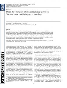
Figure 1. A photograph of vehicle level EMC testing.
135
Figure 2. A photograph of system level EMC testing.
and/or vehicle EMC testing and avoids costly consequences and time-consuming redesigns. The key contribution of this paper is the introduction of EMC modeling at the early stage of an automotive system design as well as outlining the necessary steps to create an accurate model. Real world data of radiated emission (RE) measurements and EMC simulation of a general automotive application show the benefits of EMC modeling from system optimization to catching a potential failure early at the system design stage. This paper is organized as follows. Section 2 describes the theory of operation of the studied system, shows time-domain measurements of the electronic control unit ECU signals that contribute to EMC emissions, and describes in detail the EMC lab test-setup. Section 3 provides an overview of the EMC modeling structure. Section 4 describes modeling of the motor driver and the related signal path from battery to load. Section 5 describes modeling of the microcontroller effect on radiated emissions. Section 6 compares EMC lab data and simulation results. Finally, conclusions are presented in Sections 7. 2. SYSTEM DESCRIPTION, TIME DOMAIN MEASUREMENTS, AND EMC LAB TEST-SETUP An electronic control unit (Figure 3) controls an external load (brushed DC-motor). The ECU varies the voltage to the motor through pulse width modulation PWM and provides an output to the high side of the load at a frequency of 9.6 kHz. The ECU includes a linear voltage regulator to supply a suitable 5 V power to the microprocessor that
136
Sharaa, Aloi, and Gerl Electronic Control Unit VPWR
Power Supply
Reset
5V
Mot + IN
Motor Driver
Microprocessor Mot -
Shield Gnd Gnd
Figure 3. ECU block diagram. controls the driver circuit which in turn controls the DC-motor. Figure 4 through Figure 7 show the 9.6 kHz output signal and its rise and fall times and the 8 MHz micro clock signal. These signals on board are necessary to be captured for the accuracy of the EMC model. Per CISPR25 and car manufacturer standards [11], the ECU and the harness are mounted on a table with conductive surface, separated by insulation material as shown in Figure 8. More details about the same standards and the test-setup of a component level EMC testing that automotive suppliers are required to pass before car manufacturers perform vehicle level EMC testing is shown in Figure 9. The figure shows the location of the antenna, ECU, harness, load, power source, and other important details about the test-setup. According to CISPR25, the electrical load can be cloaked as shown in Figure 8 or placed outside the RE chamber [11]. The intention is to measure radiated emissions from the ECU and harness only. In this case, the electric motor is shielded and attached to the conductive
Progress In Electromagnetics Research B, Vol. 11, 2009
137
Figure 4. Micro clock signal (frequency = 8 MHz).
Figure 5. Output signal at Mot+ (frequency = 9.6 kHz and Dutycycle = 53%).
138
Sharaa, Aloi, and Gerl
Figure 6. Rise time of the output signal at Mot+ (rise time = 1.1 µs). table to ensure that the RE measurement will not be disturbed by load emissions. CISPR25 standards are to test for the following frequency ranges using the following antennas [11]: - Rod Antenna Range: 150 KHz–30 MHz. - Biconical Antenna Range: 30 MHz–200 MHz, polarization vertical and horizontal. - Log Range: 200 MHz–1 GHz, polarization vertical and horizontal. - Horn Range: 1 GHz–2.5 GHz, polarization vertical and horizontal. For the purpose of EMC modeling, we only tested for Rod range and Biconical range with vertical polarization. The test-setup details according to CISPR25 [11] are as follows: 1. The control module is connected to the motor, battery+, and battery− through a 2 m harness. 2. The cables are all in one bundle along the 2 m long harness. Only the motor lines (Mot+, Mot−) are twisted and shielded and the shielding is connected to the ECU ground. 3. As shown in Figures 8 and 9, the ECU is at one end and the motor and battery are at the other end.
Progress In Electromagnetics Research B, Vol. 11, 2009
139
Figure 7. Fall time of the output signal at Mot+ (fall time = 1.246 µs). 4. The ECU and harness are mounted on a table with conductive surface, separated by insulation material. 5. The thickness of the insulation material is 5 cm (Figure 9). 6. The antenna is positioned at a distance of 1 m from the center of the harness (Figure 9). 7. Rod antenna is used to measure emissions for frequencies < 30 MHz and it is at the same height as the height of the table, which is 900 mm from ground. For frequencies between 30 MHz and 200 MHz, the antenna used is the Bicon antenna and it is at height 250 mm above the table and the polarization of the antenna is vertical (Figure 9). 3. EMC MODELING STRUCTURE In order to have an accurate EMC model, EMC simulation tools are utilized as they allow importing and handling of PCB and cable harness designs. These tools contain a field solver, which models structures for signal and power integrity [3]. Also, the tools contain a network simulator that understands Spice circuits. Utilizing a schematic editor, the field solver models the design components and external
140
Sharaa, Aloi, and Gerl
Figure 8. A photograph of the ECU, harness, and load inside the EMC chamber.
Figure 9. Illustration of a test-setup (side view and top view respectively). circuits [6, 8]. IBIS wave models are connected to simulate circuits and harnesses in time or frequency domain. During simulation, the geometric and electric data are stored together for radiation analysis.
Progress In Electromagnetics Research B, Vol. 11, 2009
141
The actual PCB layout of the ECU (Figure 10) is imported into the PCB modeling tool. This tool utilizes modeling techniques such as 2D MoM (Method of Moments) and 3D PEEC (Partial Element Equivalent Circuit). It has the option of analyzing in frequency or time domain and the option to use 2D or 3D line models for transmission line simulations and power and ground analyses. Dielectric losses, skin effect, and any structural EMC issues are all included in the built-in simulator.
Figure 10. Electronic control unit (ECU) layout. The cable modeling tool utilizes 2D MoM modeling technique. It has the option of analyzing in both frequency and time domain. Similar to the PCB modeling tool, dielectric losses, skin effect, and any structural EMC issues are all included in the built-in simulator. The tool can model twisted pairs, shielded cables, coaxial cables, ribbon cables, and other kinds of cables. Figure 11 shows the simulation configuration. Additionally, IBIS and Spice models of the active components such as the micro, motor driver, micro clock, zeners, and diodes are developed using various tools such as SPICE and SABER or models are obtained from the IC suppliers. The twisted and shielded harness of the motor lines (Mot+, Mot−) is characterized and imported into the model. The board signals shown in Figure 4 through Figure 7 are incorporated as well. The brushed DC motor has been electrically modelled as shown in Figure 13 to maintain the actual system signal flow in the model. As mentioned earlier, no EMC model is developed for the motor as its emissions are suppressed by the cloak covering it, which is attached to the conductive table (ground plane).
142
Sharaa, Aloi, and Gerl
Figure 11. Simulation configuration.
Figure 12. Measurement of the motor inrush and steady state current. To model the current path, it is required to extract the geometric structure of the nets and model the structures with corresponding capacitance and inductance values. The geometric structures are located 5 cm above the ground plane as shown in Figure 9. Additionally, relevant passive component values need to be added such as capacitors and inductors of the electronic circuits. Simply adding these values is an issue in the higher frequency range, because a capacitor for instance acts as an inductor above a given frequency point [12]. This is not an issue when simulating the effect of the motor driver on emissions as it is running at low frequency, however the parasitic characteristic of the components is needed for the accuracy of the high frequency simulation. Figure 14 shows the 3D (PEEC) Mesh view of the PCB, it shows the inner layers and the vias. The blue elements in the figure represent
Progress In Electromagnetics Research B, Vol. 11, 2009
143
Figure 13. Motor electrical model. capacitive areas and are translated into SPICE equivalent capacitances and conductances. The red elements represent inductive segments and are translated into SPICE equivalent inductances and resistances. Two sources inside the control module are the main cause of radiated emissions. Thus, modeling is done in two separate steps: 1. The motor driver, which controls the DC-motor via two transmission lines (Mot+, Mot−). 2. The microprocessor and its external clock. The inner switching activity causes disturbances on the PCB’s power lines and it can be emitted by the connected cables. 4. MODELING OF THE MOTOR DRIVER AND SIGNAL PATH The approach is to model the radiated emissions caused by the motor driver and the associated circuitries along the path from battery to the DC motor. The simulation setup consists of five separate models connected together: 1. Electronic circuit motor driver model.
144
Sharaa, Aloi, and Gerl
Figure 14. Stretched and rotated 3D (PEEC) mesh view of the PCB. 2. Model of the net structures on the board. 3. DC motor model. 4. Battery model with the Line Impedance Stabilization Network LISN attached. 5. Harness model. The simulation schematic for the first task is shown in Figure 15. Motor Driver Path Model: The strategy is to model the current path starting at the battery connection through the LISN and the two power lines connected to the board. Because of the low frequency spectrum of the motor driver PWM (Figure 16), the model of the board as shown in Figure 15 is only net VPWR and GND, which are considered as structures with parasitic influence. This means that MOT− and GND are considered to have the same potential. For both VPWR and GND nets, the parasitic capacitances to the ground plane and the mutual capacitance between two nets are calculated using the simulation tool to give (Cgnd = 15 pF, Cvpwr = 0.3 pF, and Cgnd − vpwr = 6 pF). All electronic components in the current path starting at VPWR are taken into account. Since the nominal values are known and the parasitic characteristics of those components are unknown, we made the following assumptions:
Progress In Electromagnetics Research B, Vol. 11, 2009
145
Figure 15. Model of the motor driver circuit and the path from battery to the DC motor.
Figure 16. Motor driver PWM frequency spectrum.
146
Sharaa, Aloi, and Gerl
- Capacitance of 1 pF in parallel and 10 mohms in series to the inductor on board. - Inductance of 1 nH and 10 mohms in series to all capacitors. The motor driver is modeled as a controlled switch according to the measured output signals (Figure 5 through Figure 7). The wire between the ECU and the motor is modeled using a screened double wire cable. The transfer impedance of the inner side of the harness shield to the outer side is assumed to be the transfer impedance of a standard coax cable. As mentioned earlier, the shield is connected to the ECU ground and is not connected on the motor side. To calculate the radiated field, the summation of the currents in the cable harness is required. The calculation is done in time domain and then it is converted into frequency domain. To calculate the electric field, a radiation simulation tool is used. According to the test-setup shown in Figure 9, the currents are taken as impressed field sources and the electric field is calculated at the location of the Rod antenna which is 1 m away from the center of the harness and at the same height as the ground plane (conductive table). PCB Model: The board model consists of three capacitances: - Self capacitance between the net ground and the ground plane (Cgnd = 15 pF). - Self capacitance between the net VPWR and the ground plane (Cvpwr = 0.3 pF). - Mutual capacitance between ground and VPWR (Cgnd − vpwr = 6 pF). DC Motor Model: To electrically model the DC brushed motor, measurements of the motor inrush and steady state currents are taken as shown in Figure 12, then SABER simulation tool is used to develop the motor model. The resulted model is shown in Figure 13. The model components are: - Rstall = 0.437 Ohms - R1 = 1.463 Ohms - Cinertia = 39.5 mF - Larmature = 154 µH Battery Model and LISN: The model of the battery is an ideal voltage source of 13.5 V. Battery negative pole is connected to the ground plane and the connection is assumed to be ideal. Both LISN − and LISN + are connected to Battery − and Battery + respectively and they are modeled with ideal inductors with values of 5 mH. Harness Model: The model of the harness consists of a twistedshielded cable for MOT+ and MOT− and separate wires not shielded
Progress In Electromagnetics Research B, Vol. 11, 2009
147
for VPWR and GND (Figure 17). The wires are 2 m long and 5 cm above the ground plane (Figure 9). Figure 17 shows the cross section of the harness bundle. The two separate wires have a diameter of 1.4 mm and εr of 2.1. The twisted wires inside the shield have a diameter of 2 mm. The diameter of the shield (inner side) is 6 mm and its εr is assumed to be 1 (non-dielectric material). The transfer impedance of the shield is an important parameter and the transfer inductance of 0.1 nH/m is assumed to be the essential part of the transfer impedance. In the simulation schematic (Figure 15), only the shielded cable model is shown in the harness model, which is subcircuit X2 with six terminals. The power lines between model 2 and model 4 are included only in the actual simulation and they are integrated in subcircuit X2 but not shown in the model to simplify the schematic representation. 5. MODELING OF THE MICROCONTROLLER EFFECT ON EMISSIONS The approach is to model the radiated emissions of the ECU caused by the microcontroller. The simulation setup consists of four separate
Figure 17. Cross-section of the harness over ground plane.
148
Sharaa, Aloi, and Gerl
models connected together: 1. Model of the microcontroller supply pins. 2. Model of the net structures on the board. 3. Model of the harness. 4. Battery model with the LISN attached. The simulation schematic for the second modeling task is shown in Figure 18.
Figure 18. Model of the microcontroller effect on emissions. The strategy is to model the current path starting at the battery connection through the LISN and the two power lines connected to the board to the microcontroller power supply. The GND (0 V), VPWR (13.5 V), and VCC (5 V) nets are extracted from the PCB (Figure 19). The parasitic characteristics (inductive and capacitive parameters) of these nets are determined and an equivalent circuit is generated (Figure 20). The self capacitance CGND (15 pF) from net ground to the ground plane is included in the equivalent circuit model as it is essential for the resulting common mode current. Additionally, the capacitors on board are taken into account along with their estimated parasitic values (Equivalent Series Resistance ESR and Equivalent Series Inductance ESL).
Progress In Electromagnetics Research B, Vol. 11, 2009
149
To calculate the radiated field, the summation of the currents in the cable harness is required. The calculation is done in time domain and then it is converted into frequency domain. To calculate the electric field, a radiation simulation tool is used. According to the test-setup shown in Figure 9, the currents are taken as impressed field sources and the electric field is calculated at the location of the Biconical antenna which is 1 m away from the center of the harness and 250 mm above the ground plane (conductive table). The model for VCC is an ideal voltage source of 5 V. The negative pole is connected to ground (0 V ideal). Both LISN − and LISN + are modeled with ideal inductors of 500 nH and a capacitance of 100 nF to ground. To model the harness, only three wires are included in the bundle with 2 m long. Figure 21 shows the cross-section of the bundle. The
Figure 19. Extracted nets of the PCB: VCC, VPWR in red, GND in green.
150
Sharaa, Aloi, and Gerl
Figure 20. Equivalent circuit of the PCB structures with models of board capacitors. two small wires are the plus and minus from the PCB to battery, the large wire simulates the outer layer of the shielded wire. 6. LAB RE MEASUREMENTS AND EMC SIMULATION RESULTS Figure 22 shows RE measurement of the system shown in Figure 8 using Rod antenna and the simulation results of the equivalent model. Figure 23 shows RE measurement using Bicon antenna and the simulation results of the equivalent model. As shown in the figures, simulation results and lab measurements show high conformity.
Progress In Electromagnetics Research B, Vol. 11, 2009
151
Figure 21. Cross section of the harness.
Figure 22. RE measurement using Rod antenna and simulation results of the equivalent EMC model.
152
Sharaa, Aloi, and Gerl
Figure 23. RE measurement using Bicon antenna and simulation results of the equivalent EMC model. 7. CONCLUSIONS In today’s technology environment, getting products to market quickly at minimum cost is critical to all electronic product manufacturers. Waiting for EMI compliance and achieving EMC RE first pass success is a difficult task. According to Intertek Testing Services Inc., a large percentage of electronic products fail to meet their target EMC requirements the first time they are tested and despite the growing awareness of EMC design considerations, EMC test failure rates are still around 50% [13]. This issue has a great impact on cost and time, such as time to market and testing cost. As outlined in the real world case presented in this paper, EMC modeling and simulation are used to model an EMC test-setup according to CISPR25 standards [11] to predict the EMC behavior of a general automotive system. The paper also outlines the modeling steps and describes in detail the modeling procedure. These steps need to be
Progress In Electromagnetics Research B, Vol. 11, 2009
153
specified and followed to ensure effective modeling of complex systems that include antennas, electronic units, and cable harnesses. Even though EMC modeling and simulation will not replace the validation of the final product, however, it reduces the risk of EMC failure and avoids potential delays on a scheduled launch of new products. ACKNOWLEDGMENT This work was done with the support of Visteon Corporation, SimLab Software GmbH, and Oakland University. Thanks to Visteon and STMicroelectronics engineers for their contribution in providing models for the electronic components and special thanks to SimLab engineers for the help with modeling and simulation. REFERENCES 1. Hurst, G., A. Stelzer, and J. Runnells, “Design for compliance: It’s about time [and money!],” Proceedings of IEEE Electromagnetic Compatibility International Symposium, Santa Clara, CA, 630– 634, Aug. 2004. 2. Wu, T., Electromagnetic Compatibility: EMC Requirement for Electronic Systems, University of Central Florida. 3. Hubing, T., J. Drewniak, T. Drewniak, T. van Doren, and N. Kashyap, “An expert system approach to EMC modeling,” Proceedings of IEEE Electromagnetic Compatibility International Symposium, 200–203, Santa Clara, CA, Aug. 1996. 4. Neumayer, R., A. Stelzer, F. Haslinger, J. Held, F. Schinco, and R. Weigel, “Continuous simulation of system-level automotive EMC problems,” Proceedings of IEEE Electromagnetic Compatibility International Symposium, 409–413, Boston, MA, Aug. 2003. 5. Neumayer, R., A. Stelzer, F. Haslinger, G. Steinmair, M. Troscher, J. Held, B. Unger, and R. Weigel, “Numerical EMC simulation for automotive applications,” Proceedings of IEEE Electromagnetic Compatibility International Symposium, 459–464, Zurich, Switzerland, Feb. 2003. 6. Haslinger, F., B. Unger, R. Weigel, M. Maurer, and M. Troscher, “EMC modeling of nonlinear components for automotive applications,” Proceedings of IEEE Electromagnetic Compatibility International Symposium, 419–424, Zurich, Switzerland, Feb. 2001. 7. Neumayer, R., A. Stelzer, and R. Weigel, “Equivalent circuit modeling using frequency-domain subspace system identification,”
154
8.
9.
10.
11. 12. 13.
Sharaa, Aloi, and Gerl
Proceedings of IEEE Electromagnetic Compatibility International Symposium, 1066–1069, Istanbul, Turkey, May 2003. Englmaier, A. and B. Scholl, “EMC modelling strategy for automotive applications,” Int. SimLab User Conference 2000, Munich, Nov. 2000. Noble, I. E., “Electromagnetic compatibility in the automotive environment,” Science, Measurement and Technology, IEE Proceedings, 252–258, July 1994. Calvet, S., C. Huet, J. Levant, C. Maro, J. Perrin, and E. Sicard, Cookbook for Integrated Circuit Electromagnetic Model (ICEM), Oct. 2001. CISPR 25, International Electrotechnical Commission, 2nd edition, 2002–08. Paul, C. R., Introduction to Electromagnetic Compatibility, New York, 1992. Gubisch, R., Why 50% of Products Fail EMC Testing the First Time, Intertek Testing Services NA, Inc.