tum dot circuit containing just a single conduction elec- tron, with the ability to read out the quantum state of the electron. Few-electron quantum dots have been ...
Experiments And Simulations On A Few-Electron Quantum Dot Circuit With Integrated Charge Read-Out R. Hanson∗ , J.M. Elzerman∗ , L.H. Willems van Beveren,∗ , L.M.K. Vandersypen∗ , L.-X. Zhang,† , P. Matagne† , J.P. Leburton† and L.P. Kouwenhoven∗ ∗
Kavli Institute of Nanoscience Delft and ERATO Mesoscopic Correlation Project, P.O. Box 5046, 2600 GA Delft, The Netherlands † Beckman Institute for Advanced Science & Technology and Department of Electrical and Computer Engineering, University of Illinois at Urbana-Champaign, Urbana, Illinois 61801 Abstract. We report measurements and simulations on a fully tunable double quantum dot circuit, integrated with two quantum point contacts that serve as charge detectors. The circuit is defined in a two-dimensional electron gas by means of surface gates on top of a GaAs/AlGaAs heterostructure. Full control over the electron number (down to zero), the dot-lead coupling and the inter-dot tunnel coupling is experimentally demonstrated. Computer simulations can map out the double dot charging diagram and show that the charge sensitivity can be significantly enhanced by improving the design of the circuit.
INTRODUCTION The spin of single electron confined in a semiconductor quantum dot [1] is a promising candidate for a scalable quantum bit [2], since it combines the single-electron charge degree of freedom (which is easy to manipulate with electrical voltages) with the spin degree of freedom (which is expected to exhibit a long coherence time). For the control of one-electron quantum states by electrical voltages, the challenge is to realize an appropriate quantum dot circuit containing just a single conduction electron, with the ability to read out the quantum state of the electron. Few-electron quantum dots have been realized in selfassembled structures [3] and also in small vertical pillars defined by etching [4]. The disadvantage of these types of quantum dots is that they are hard to integrate into circuits with a controllable coupling between the elements, although integration of vertical quantum dot structures is currently being pursued. An alternative candidate is a system of lateral quantum dots defined in a two-dimensional electron gas (2DEG) by surface gates on top of a semiconductor heterostructure [1]. Here, integration of multiple dots is straightforward by simply increasing the number of gate electrodes. In addition, the coupling between the dots can be controlled, since it is set by gate voltages. The challenge is to reduce the number of electrons to one per quantum dot. This has long been impossible, since reducing the electron number decreases at the same time the tunnel coupling, resulting in a current too small to be measured [5].
In the first part of this work, we experimentally demonstrate double quantum dot devices containing a voltage-controllable number of electrons down to a single electron [6]. We have integrated these devices with charge detectors that can read out the charge state of the double quantum dot with a sensitivity much better than a single electron charge. The measurements show that even in the few-electron regime, both the coupling to the leads and the interdot tunnel-coupling can be fully controlled. In the second part, we present computer simulations of the devices. The charging diagram for the first two electrons in the double dot circuit is calculated [7]. Then, we use the simulations to test different circuit designs. We find that by proper design of the circuit the charge sensitivity can be significantly enhanced [8].
EXPERIMENTS Device Parameters We study two nominally identical devices, both as shown in Fig. 1a. They are made from a heterostructure consisting of four different layers of semiconductor materials (from top to bottom): a 50 Å thick n-type (ND = 1.5 × 1018 cm−3 ) GaAs layer, a 650 Å thick ntype (ND = 1.0 × 1018 cm−3 ) Al0.27 Ga0.73 As layer, a 200 Å thick undoped Al 0.27 Ga0.73 As layer, and a 1000 nm thick GaAs layer. The 2DEG, which has a density ns = 2.9 × 1011 cm−2 , is formed at the interface between
a
IDOT
200 nm
Q-R
Q-L
IQPC
IQPC source1
L PL M PR R
drain2
b
dots using standard Coulomb blockade experiments [1], and find that the energy cost for adding a second electron to a one-electron dot is 3.7 meV. The excitation energy (i.e. the difference between the first excited state and the ground state) is 1.8 meV at zero magnetic field. For a two-electron dot the energy difference between the singlet ground state and the triplet excited state is 1.0 meV at zero magnetic field. Increasing the field (perpendicular to the 2DEG) leads to a transition from a singlet to a triplet ground state at about 1.7 Tesla.
5
4
3
d
dIQPC/dVM I DOT (pA) (arb. units)
30
2
transport
0
2
G (e /h)
c
source2
T
IQPC (nA)
drain1
1
0 -0.50
-0.55
-0.60
VQ-L (V)
-0.65
QPC -1.25
-1.30
-1.35
-1.40
VM (V)
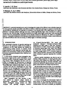
FIGURE 1. (a) Scanning Electron Micrograph of the metallic surface gates. White dotted circles indicate the two quantum dots. White arrows show the possible current paths. A bias voltage, VDOT , can be applied between source 2 and drain 1, leading to current through the dots, IDOT . A bias voltage, VSD1 (VSD2 ), between source 1 (source 2) and drain 1 (drain 2), yields a current, IQPC , through the left (right) QPC. (b) Conductance, G, of the left QPC versus the gate voltage, VQ−L , showing the last quantized plateau and the transition to complete pinch-off. The cross indicates the point of highest charge sensitivity. (c) Current through the left QPC, IQPC , versus leftdot gate voltage, VM . (VSD1 = 250 µ V, VDOT = 0, VSD2 = 0). The steps, indicated by the arrows, correspond to a change in the electron number of the left dot. Encircled inset: the last step (50 pA high), with the linear background subtracted. (d) Upper part: Coulomb peaks measured in transport current through the left dot. Shown is IDOT versus VM with VDOT = 100 µ V. Lower part: changes in the number of electrons on the left dot, measured with the left QPC. Shown is dIQPC /dVM versus VM (VSD1 = 250 µ V, VDOT = 0).
the undoped AlGaAs layer and the GaAs layer (900 Åbelow the surface). Both devices consist of a double quantum dot and two quantum point contacts (QPCs). The layout is an extension of previously reported single quantum dot devices [5]. The double quantum dot is defined by applying negative voltages to the 6 gates in the middle of the figure. Gate T in combination with the left (right) gate, L (R), defines the tunnel barrier from the left (right) dot to drain 1 (source 2). Gate T in combination with the middle, bottom gate, M, defines the tunnel barrier between the two dots. The narrow "plunger" gate, PL (PR ), on the left (right) is used to change the electrostatic potential of the left (right) dot. The plunger gates can be connected to a coaxial cable so that we can apply high-frequency signals. In the present experiments we do not apply dc voltages to PL . In order to control the number of electrons on the double dot, we use gate L for the left dot and PR or R for the right dot. All measurements are performed at a temperature of 10 mK. We first study sample 1. We characterize the individual
Charge Detection With A QPC In addition to current flowing through the quantum dot, we can measure the charge on the dot using one of the QPCs [9, 10]. We define only the left dot (by grounding gates R and PR ), and use the left QPC as a charge detector. The QPC is formed by applying negative voltages to Q-L and L. This creates a narrow constriction in the 2DEG, with a conductance, G, that is quantized when sweeping the gate voltage VQ−L . The plateau at G = 2e2 /h and the transition to complete pinch-off (i.e. G = 0) are shown in Fig. 1b. At the steepest point, where G ≈ e2 /h, the QPC-conductance has a maximum sensitivity to changes in the electrostatic environment, including changes in the charge of the nearby quantum dot. As can be seen in Fig. 1c, the QPC-current, I QPC , decreases when we make the left-dot gate voltage, V M , more negative. Periodically this changing gate voltage pushes an electron out of the left dot. The associated sudden change in charge increases the electrostatic potential in the QPC, resulting in a step-like structure in I QPC (see expansion in Fig. 1c, where the linear background is subtracted). So, even without passing current through the dot, I QPC provides information about the charge on the dot. To enhance the charge sensitivity we apply a small modulation (0.3 mV at 17.7 Hz) to VM and use lock-in detection to measure dIQPC /dVM [10]. Figure 1d shows the resulting dips, as well as the corresponding Coulomb peaks measured in the current through the dot. The coincidence of the two signals demonstrates that the QPC indeed functions as a charge detector. From the height of the step in Fig. 1c (50 pA, typically 1-2 percent of the total current), compared to the noise (5 pA for a measurement time of 100 ms), we can estimate the sensitivity of the charge detector to be about 0.1e, with e being the single electron charge. The important advantage of QPC charge detection is that it provides a signal even when the tunnel barriers of the dot are so opaque that I DOT is too small to measure [9, 10]. This allows us to study quantum dots even while they are virtually isolated from the leads.
Double Dot In The Few-Electron Regime
Tunability Of The Double Dot Circuit In measurements of transport through lateral double quantum dots, the few-electron regime has never been reached [12]. The problem is that the gates, used to deplete the dots, also strongly influence the tunnel barriers. Reducing the electron number would always lead to the Coulomb peaks becoming unmeasurably small, but not necessarily due to an empty double dot. The QPC detectors now permit us to compare charge and transport measurements. Figure 3a shows I DOT versus VL and VPR , with the dotted lines extracted from the measured charge lines in Fig. 2b. In the bottom left region the gates are not very negative, hence the tunnel barriers are quite open.
VL (V)
-1.1 00
-1.0
-0.9 0.0
-0.2
-0.4
-0.6
VPR (V)
b 01
-1.02
VL (V)
Next, we study the charge configuration of the double dot, using the QPC on the right as a charge detector. We measure dIQPC /dVL versus VL , and repeat this for many values of VPR . The resulting two-dimensional plot is shown in Fig. 2a. Dark lines signify a negative dip in dIQPC /dVL , corresponding to a change in the total number of electrons on the double dot. Together these lines form the well-known "honeycomb diagram" [11, 12]. The almost-horizontal lines correspond to a change in the electron number in the left dot, whereas almost-vertical lines indicate a change of one electron in the right dot. In the upper left region the "horizontal" lines are not present, even though the QPC can still detect changes in the charge, as demonstrated by the presence of the "vertical" lines. We conclude that in this region the left dot contains zero electrons. Similarly, a disappearance of the "vertical" lines occurs in the lower right region, showing that here the right dot is empty. In the upper right region, the absence of lines shows that here the double dot is completely empty. We are now able to count the absolute number of electrons. Figure 2b shows a zoom-in of the few-electron region. Starting from the "00" region, we can label all regions in the honeycomb diagram, e.g. the label "21" means two electrons in the left dot and one in the right. Besides the dark lines, also short white lines are visible, signifying a positive peak in dI QPC /dVL . These white lines correspond to a charge transition between the dots while the total electron number remains the same. (The positive sign of dIQPC /dVL can be understood if we note that crossing the white lines by making VL a little more positive means moving an electron from the right to the left dot, which increases IQPC . Therefore the differential quantity dIQPC /dVL displays a positive peak.) The QPC is thus sufficiently sensitive to detect inter-dot transitions.
a
-1.00
00
12 11 10
-0.98 22 21
-0.96 -0.15
-0.20 -0.25 -0.30
VPR (V) FIGURE 2. (a) Charge stability diagram ("honeycomb") of the double quantum dot, measured with Q-R. A modulation (0.3 mV at 17.77 Hz) is applied to gate L, and dIQPC /dVL is measured with a lock-in amplifier and plotted in grayscale versus VL and VPR . The bias voltages are: VSD2 = 100 µ V and VDOT = VSD1 = 0. The label "00" indicates the region where the double dot is completely empty. (b) Zoom-in of Fig. 2a, showing the honeycomb pattern for the first few electrons in the double dot. The black labels indicate the number of electrons in the left and right dot.
Here the resonant current at the charge transition points is quite high (∼ 100 pA, dark gray), and also lines due to cotunneling are visible [12]. Towards the top right corner the gate voltages become more negative, thereby closing off the barriers and reducing the current peaks (lighter gray). The last Coulomb peaks (in the dashed square, and in Fig. 3b) are faintly visible (∼ 1 pA). Apart from a slight shift, the dotted lines nicely correspond to the regions where a transport current is visible. We are thus able to measure transport through a one-electron double quantum dot. Even in the few-electron regime, the double dot remains fully tunable. By changing the voltage applied to gate T , we can make the tunnel barriers that define the double dot more transparent, leading to a larger current through the device. We use this procedure to increase the current at the last two triple points. For the gate voltages used in Fig. 3b, the resonant current is very small (< 0.5 pA), and the triple points are faintly visible. By making VT less negative, the resonant current becomes about 5
a
a
b 01
-1.02
-0.95
weak coupling
b -1.10
strong coupling
00
-1.00
11
VR (V)
VL (V)
00
c
12
-0.90
-1.05
00
10 -0.98
22
d
21 -0.96
-0.85
-1.00
-0.85 -0.15
-0.20
-0.25
-0.30
-0.90 -0.95 VL (V)
-1.00
-1.05 -1.10 VL (V)
VPR (V)
FIGURE 3. (a) Transport through the double dot in the same region as Fig. 2b. Plotted in logarithmic grayscale is IDOT versus VL and VPR , with VDOT = 100 µ V and VSD1 = VSD2 = 0. The dotted lines are extracted from Fig. 2b. Light color corresponds to zero current and black corresponds to ∼ 100 pA. Inside the dashed square, the last Coulomb peaks are visible (∼ 1 pA). (b)-(d) Close-up of the region inside the dashed square in (a), showing the last two triple points before the double dot is completely empty. Tuning the gate voltages increases the current from < 0.5 pA (b) to 5 pA (c), and finally to 70 pA (d).
pA (Fig. 3c). The cotunneling current is not visible, and the two triple points are clearly separated. By changing VT even more, the current at the last triple points can be increased to ∼ 70 pA (Fig. 3d). For these settings, the triple points have turned into lines, due to the increased cotunneling current. This sequence demonstrates that we can tune the double dot from being nearly isolated to being very transparent. We can also control the inter-dot coupling, by changing the voltage applied to gate M. This is demonstrated with a QPC charge measurement using sample 2. We apply a square wave modulation of 3 mV at 235 Hz to the rightmost plunger gate, PR , and measure dIQPC /dVPR using a lock-in amplifier. Figure 4a shows the familiar honeycomb diagram in the few-electron regime. All lines indicating charge transitions are very straight, implying that for the gate settings used, the tunnnel-coupling between the two dots is negligible compared to the capacitive coupling. This is the so-called "weak-coupling" regime. (We note that the double dot as a whole is still quite well-coupled to the leads, so that the total number of electrons can change, as demonstrated by the regular shape of the honeycomb pattern[13].) By making V M less negative, the tunnel barrier between the two dots is made more transparent, and an "intermediate-coupling" regime is reached (not shown). Here, most lines are still straight, except for the most positive voltages, where they are slightly bent. This signifies that the inter-dot tunnel-coupling is comparable to the capacitive coupling. If we make VM even less negative, we reach the strongcoupling regime (Fig. 4b). In this case, all lines are very
FIGURE 4. Controlling the inter-dot coupling with VM in sample 2. dIQPC /dVPR is plotted in grayscale versus VL and VR . A magnetic field of 6 Tesla is applied in the plane of the 2DEG. (a) Weak-coupling regime, where all dark lines, indicating charge transitions, are straight. The tunnel-coupling between the two dots is negligible compared to the capacitive coupling. (b) Strong-coupling regime, where VM is 0.17 V less negative than in (a), such that all lines are very curved. This implies that the tunnel-coupling is dominating over the capacitive coupling.
curved, implying that the tunnel-coupling is dominating over the capacitive coupling. Thus the double dot behaves more like a single dot in this regime.
SIMULATIONS Simulation Of The Charging Diagram We use computer modeling to simulate the charging of the quantum states in the laterally coupled quantum dot (LCQD) and the corresponding electrostatic variation in the QPC [7, 8]. For this purpose, we solve coupled three-dimensional Kohn-Sham [14] and Poisson equations self-consistently to obtain the quantum states in the LCQD region, while outside this region the charge density is determined by solving Poisson equation within the Thomas-Fermi approximation [16, 7]. The above differential equations are solved on a non-uniform threedimensional (3D) mesh using the finite element method (FEM) with proper boundary conditions, described elsewhere [15, 16]. We use a variation on the Slater formula [17, 18] to determine the stable charge configuration in the LCQD, so that charging occurs when
εLUO (1) − EF = EF − εLUO (0)
(1)
where εLUO (α ) is the eigenenergy of “the lowest unoccupied orbital,” with occupancy α , and E F is the Fermi energy. (This variation was justified in Ref. [16]). Figure 5 shows the conduction band edge profiles in the xy-plane at the 2DEG interface (contour plot, Fig. 5a) and in the z-direction (Fig. 5b) under the condition VL = VR = VQPC−L = VQPC−R = VM = −0.585 V, VT =
(a)
Optimizing The Charge Sensitivity
y (A )
2000 1000 0 -1000 -2000
-6000 -4000 -2000
0
2000 4000 6000
x (A )
(b) 1.0
Ec (eV)
0.8
0
1000
0.6
2000
z (A)
3000
0.4 0.2 0.0
-0.2 0
1000
2000
3000
z (A )
4000
5000
FIGURE 5. Conduction band edge profile in the LCQD-QPC structure: (a) contour plot in the xy-plane at the 2DEG interface (the dashed rectangle shows the location of the dots), (b) along the z-direction at the centre of the right dot, (x,y) = (1300 Å,150 Å), with the inset showing the shape of the ground state wavefunction (VPL = VPR = −0.15 V, zero electrons).
−0.9 V, VPL = VPR = −0.15 V and zero electrons in the dots. The Fermi level is set at zero throughout the device at the temperature T = 4 K. The LCQD region and the QPC region with low equipotential-line density are clearly visible in Fig. 5a. The outer energy barrier for the LCQD is ∼ 110 meV whereas the energy barrier between the dots is ∼ 9 meV. A large negative T gate bias is used to prevent the wavefunctions from leaking into the external reservoirs, which clearly defines the LCQD region. Also, clearly visible are the QPC constrictions in the potential at x ∼ ±4900 Å and y ∼ 0 Å. The confinement along the z-direction is achieved by a quasitriangular shaped well shown in Fig. 5b, for which the relaxation of the potential to zero-field is not shown at the far end (substrate) of the device. Due to the strong confinement in the triangular well, only the ground state along the z-direction is occupied (the shape of the ground state wavefunction along the z-direction is shown in the inset in Fig. 5b). Starting from an empty double dot, we detect the single-electron charging events by monitoring the energy of the dot as a function of the voltage on the two plunger gates. By following different charging paths, and connecting the points of single-electron charging, we can draw the "honeycomb" charging diagram (for an extensive description see Ref. [7]). We find that the voltage separation between the two triple points ∆VPR = 7.7 mV, which is comparable to the experimental result ∼ 7.4 mV.
Computer simulations provide an excellent tool to test different designs of the quantum dot circuit, thus eliminating the need for time-consuming device fabrication and extensive test measurements. Here, we use computer simulations to find the sensitivity of the QPC conductance to single-electron charging in the double quantum dot, for four different designs. In Fig. 6a-d, we show the different QPC gate geometries (dark dash lines in the upper panels) in a small region near the right QPC. In order to keep the symmetry of the circuit, we change the left QPC gates accordingly (not shown). Figure 6a shows the original design, while in Fig. 6b, the tips of the QPC are replaced by flat ends to form a rectangular-shaped channel. In both Fig. 6c and d, the detector is designed to have a dent in the R-gate. In Fig. 6d, the dent is placed 600 Å closer to the right dot than in Fig. 6c. In these four designs, the nearest distance between the R-gate and the QPC-R gate is maintained at 2000 Å, which implies that for design (d) the R-gate is thinner in the dent while for design (c) it is thicker outside the dent. Equipotential-energy lines (gray solid lines in Fig. 6a-d in the upper panels) are plotted under the gates showing the different conduction channel geometries caused by the different gate designs. The bias conditions for the circuit (specified in the figure captions for each case) are set at the (0,0) to (0,1) transition. Different QPC biases are compensated for by changing V PR . It is clearly seen that the conduction channels in designs (b)-(d) are more squeezed compared to the channel in design (a). In Fig. 6a and b the channels are straight, while in Fig. 6c and d they are curved towards the right dot. The lower panels in Fig. 6a-d show the potential energy profiles along the x-direction (for the same xdistance as the upper panels). The conduction channels are seen to be increasingly confined from designs (a) to (c). To obtain the charge sensitivity, we take the jump at the saddle point of the potential energy in the QPC constriction due to single-electron charging of the adjacent dot, ∆EC , and compute the relative change in conductance G of the QPC, ∆G/G, at G = e 2 /h by ∆G π =− ∆EC , h¯ ωy G
(2)
where h¯ ωy is the characteristic energy for a y-direction parabolic fitting of the potential energy near its saddle point in the constriction of the QPC [19]. The characteristic energy h¯ ωy is obtained by fitting the potential energy in the constriction of the QPC with an 11-point parabola over the distance of the QPC gate (i.e., 1000 Å) along the y-direction. We compute the absolute value of the righthand side of Eq. (2) within a wide experimental range of
(a)
the numerical values obtained that the improvement of = 73% to ∆G/G falls in the range from min(d)−max(a) max(a)
(b) 0.1
y (µm)
y (µm)
0.1
0.12
EC (eV)
EC (eV)
- 0.1
0 0.3
0.5
max(d)−min(a) min(a)
= 308%, where min(a) and max(a) denote the minimum and maximum values achieved by ∆G/G for design (a) over the investigated voltage range and similarly for design (d).
- 0.1 0.15
0
0.7
0.3
x (µm)
0.5
(d)
(c) 0.1
We thank T. Fujisawa, T. Hayashi, Y. Hirayama, S. Tarucha, T. Saku, D. Melnikov, S. De Franceschi and R. Schouten for discussions and help. This work was supported by the DARPA-QUIST program, the ONR, the EU-RTN network on spintronics, the Material Computational Center at the University of Illinois through NSF Grant DMR 99-76550 and the Dutch Organisation for Fundamental Research on Matter (FOM).
y (µm)
y (µm)
0.1
- 0.1 0.16
EC (eV)
EC (eV)
- 0.1 0.16
0
ACKNOWLEDGEMENTS
0.7
x (µm)
0 0.3
0.5
x (µm)
0.7
0.3
0.5
0.7
REFERENCES
x (µm)
FIGURE 6. (a), (b), (c) and (d): top panels: contour plots of the potential energy near the right QPC with the gate shape superimposed by dashed lines for design (a), (b), (c) and (d), respectively. Notice that equi-potentials are lower (higher) in the channel (underneath the gates). Bottom panels: potential energy profiles in the x-direction at maximum QPC constriction (y = −150 Å). Dashed lines indicate the Fermi levels. The bias conditions are, in design (a), VL = VR = VM = −0.585 V, VPR = −0.061 V; in design (b), VL = VR = VM = −0.57 V, VPR = −0.055 V; in design (c), VL = VR = VM = −0.55 V, VPR = −0.021 V; in design (d), VL = VR = VM = −0.62 V, VPR = −0.008 V. Otherwise, VPL = −0.15 V, VT = −0.9 V, and VQPC−L = VQPC−R = −0.8 V for all the designs.
QPC gate biases (−0.8 to −0.3 V), aware that the condition G = e2 /h falls within this range [8]. We find that (1) for all the designs, ∆EC decreases monotonically as VQPC−R increases, which is due to the relaxation of the QPC confinement; (2) ∆E C increases from design (a) to (d) at each QPC gate bias. Furthermore, ∆G/G is rather insensitive to VQPC for designs (a) and (b) , while it decreases monotonically as V QPC is increased for designs (c) and (d). We notice that the detector sensitivity of the original design (a) (∆G/G ≈ 2%) is in good agreement with the experimental data [6]. The minimum values of ∆G/G for designs (c) and (d) (3.67% and 5.32%, respectively) are even larger than the maximum values for designs (a) and (b) (3.07% and 3.06%, respectively) over the whole range of QPC gate biases. Hence, we conclude that for a specific QPC gate bias that achieves G = e2 /h, designs (c) and (d) have larger detector sensitivity than designs (a) and (b). We find from
1.
2. 3. 4. 5. 6. 7. 8. 9. 10. 11. 12. 13. 14. 15. 16. 17. 18. 19.
L. P. Kouwenhoven et al., in Mesoscopic Electron Transport, edited by L. L. Sohn, L. P. Kouwenhoven, and G. Schön, NATO Advanced Study Institutes, Ser. E, Vol. 345 (Kluwer, Dordrecht, Boston, 1997), pp. 105-214. D. Loss and D. P. DiVincenzo, Phys. Rev. A 57, 120 (1998). P. M. Petroff, A. Lorke, and A. Imamoglu, Phys. Today, 46 (May 2001). L. P. Kouwenhoven, D. G. Austing, and S. Tarucha, Rep. Prog. Phys. 64 (6), 701 (2001). M. Ciorga et al., Phys. Rev. B 61, R16315 (2000). J.M. Elzerman et al., Phys. Rev. B 67, 161308(R) (2003). L.-X. Zhang et al., Phys. Rev. B 69, 245301 (2004). L.-X. Zhang, J.P. Leburton, R. Hanson and L. P. Kouwenhoven, accepted for publication in Appl. Phys. Lett. M. Field, et al., Phys. Rev. Lett. 70, 1311 (1993). D. Sprinzak et al., Phys. Rev. Lett. 88, 176805 (2002). H. Pothier et al., Europhys. Lett. 17, 249 (1992). W. G. van der Wiel et al., Rev. Mod. Phys. 75, 1 (2003), see also cond-mat/0205350v2. A. W. Rushforth et al. Phys. Rev. B 69, 113309 (2004). W. Kohn and L. J. Sham, Phys. Rev. 140, A1133 (1965). P. Matagne, J.-P. Leburton, J. Destine and G. Cantraine, Comp. Mod. Eng. Sciences 1, 1 (2000). P. Matagne and J.-P. Leburton, Phys. Rev. B 65, 235323 (2002). J. C. Slater, Adv. Quantum Chem. 6, 1 (1972). S. Nagaraja, J.-P. Leburton and R. M. Martin, Phys. Rev. B 60, 8759 (1999). M. Büttiker, Phys. Rev. B 41, 7906 (1990).