IEEE Sensors Conference, Toronto, October 22-24, 2003.
Fabrication of arrays of artificial hairs for complex flow pattern recognition J.J. van Baar, M. Dijkstra, R.J. Wiegerink, T.S.J. Lammerink and G.J.M. Krijnen MESA+ Research Institute, University of Twente P.O. Box 217, 7500 AE Enschede, The Netherlands e-mail:
[email protected] fax: +31-53-489 3343
Abstract We present monolithically integrated high-density arrays of artificial hairs for flow pattern measurements based on drag force. A combined bulk/surface micromachining process has been developed to integrate the artificial hairs with capacitive read-out. First fabrication results show the possibility to fabricate out-of-plane hairs without reverting to micro-assembly technologies. This enables realisation of high-density arrays of symmetrical sensors with twodimensional sensitivity.
FABRICATION OF ARTIFICIAL HAIRS Two types of artificial hairs can be distinguished, namely hairs fabricated in the wafer plane and hairs fabricated perpendicular to the wafer plane. Fabrication of hairs in the wafer plane is most straightforward since surface micromachining techniques can be used [4]. However, although the fabrication process is straightforward, surface micromachined hairs are less interesting because they cannot easily be combined into high-density arrays. Li et al proposed to use the so-called plastic deformation magnetic assembly (PDMA) method to erect the hairs out of the wafer plane [5, 6, 7]. In the PDMA process, a magnetic field is used to bend surface micromachined beams. The beams are plastically deformed, so that they remain bent after the magnetic field is removed.
Keywords Artificial hairs, flow sensors, lifelike perception INTRODUCTION The CICADA1 project [1] aims to contribute to the scientific and technological advancements of life-like perception systems within the European Community. The project provides novel concepts for the integration of sensingperception-action functions, based on exciting scientific work on biological paradigms and state-of-the-art developments in MEMS, composite material science and electrophysiology.
An important drawback of surface micromachined hairs is that they are not symmetrical, even if they are erected out of the wafer plane. As a result, these sensors are primarily sensitive in one direction. Furthermore, the sensors take up a relatively large area of the substrate and the choice of the read-out mechanism is limited due to the restrictions imposed by the hair fabrication. Therefore, our research has focused on bulk micromachining of hairs, i.e. fabrication of the hairs in the wafer instead of on the wafer surface.
In order to create integrated sensing-perception-response systems inspired by nature, many biological paradigms are possible for inspiration, ranging from unicellular organisms to highly complex beings such as higher animals and humans. Among the many choices available, insects offer very good examples of life-like perception because they are sufficiently complex, but amenable to be characterized and quantified, so as to provide a suitable scientific and technical challenge with a realistic chance of success. In the CICADA project we will fabricate artificial hairs inspired by the hairs found on cerci of crickets [2, 3]. It is hypothesized that crickets use hairs of several lengths to detect the complex flow patterns produced by their predators. It is the aim of this work to make arrays of artificial hairs to perform comparable functions.
1
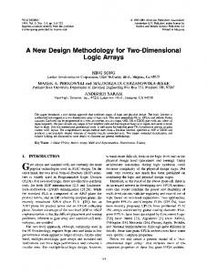
Fig. 1 shows a summary of the fabrication process that was developed for the fabrication of artificial hairs by refilling of holes created by deep reactive ion etching (DRIE). First, a 25 nm SixNy layer is deposited by low-pressure chemical vapor deposition (LPCVD). This layer ensures good adhesion of a 20 nm thin chromium layer, which is deposited on top of the SixNy layer by sputtering. After lithography and patterning chromium layer, deep holes are etched by DRIE using the chromium layer as etch mask. After stripping of the chromium layer, the deep holes are refilled by LPCVD of a 1 µm thick low-stress SixNy layer [7]. Then, the SixNy on the backside is patterned, and, finally, the silicon bulk is locally removed by wet etching in KOH so that the hairs are exposed.
Cricket Inspired PerCeption & Autonomous Decision Automata
0-7803-8133-5/03/$17.00 ©2003 IEEE
332
ways. A mechanical deformation is measured by simply measuring a change in the electrical resistance. Although an electrical current is required for the measurement, the dissipation is much lower than in the case of thermal sensing. However, the sensitivity is also rather low, which makes it less suitable for our application. Initial finite element simulations revealed that the deformation and rotation of an artificial hair due to airflow will be extremely small and a highly sensitive read-out technique is required.
1. Silicon wafer 2. LPCVD 25 nm of SixNy, Sputter 20 nm chromium layer 3. Lithography and patterning of chromium layer 4. Deep reactive ion etching (DRIE) 5. Stripping of chromium layer 6. Low pressure chemical vapor deposition (LPCVD) of SixNy 7. Photolithograhy and reactive ion etching of SixNy 8. Wet etching of silicon in KOH Fig. 1: Process sequence used for bulk micromachining of artificial hairs.
A mask was designed for the fabrication of hairs with various shapes (circle, star, cross, rectangle and triangle) and diameters, ranging from 5 to 50 µm. Fig. 2 shows photographs of fabricated circular hairs. The close-up clearly shows that the shape develops into a rectangular shape after about 100 µm, which is due to the different etching speed for different crystallographic directions. Furthermore, we see that the top of each hair is quite flat. This means that the limit of the etching process has not yet been reached: longer etching will still result in longer and hairs. The exact shape of the hairs is largely determined by process parameters.
(a)
READOUT MECHANISMS A flow of air causes a drag force on the hair. A suitable readout mechanism is needed to detect the resulting hair movement. Most micromachined flow sensors are based on thermal sensing techniques. That is, a structure is heated and temperature changes due to airflow are measured. In principle, thermal sensing techniques can also be applied to micromachined hairs, either by heating the hair itself or by heating a structure at the base which moves with the hair. However, since dissipating sensors do not lend themselves particularly well for integration into large arrays (due to power consumption and thermal issues) we have focussed on other sensing principles, which are better suited for integration.
(b) Fig. 2: Array of fabricated hairs (a) and close-up of hairs of different size (b). The flat top of the hair indicates that longer etching will still result in longer hairs.
•
Capacitive Capacitive sensing gives a much higher sensitivity than piezoresistive sensing and also the power dissipation can be extremely small. However, more complicated mechanical structures and special electronic read-out circuitry are needed. Still, capacitive sensing can in principle fulfil all performance requirements.
•
Piezoelectric Piezoelectric sensing can be far simpler than capacitive, but has the difficulty of the associated technological steps of deposition and structuring of
Besides thermal sensing, three other sensing mechanisms were considered: •
Piezoresistive Piezoresistive sensing is commonly used because of the easy fabrication and easy interfacing. For piezoresistive sensing, it is necessary to integrate a silicon resistor, which can be accomplished in several 333
velocity of 3 m/s at a height of 400 µm (boundary layer). In that case the maximum out of plane deflection of the circular plate is in the order of 20 nm as shown in Fig. 4. The hair-tip moves 40 nm in the direction of the airflow.
piezoelectric materials. Piezoelectric sensing has the advantage that power consumption is negligible. This will become important because when the number of sensors increases the overall power consumption and/or the dissipation per unit of area may become too high for structures to be practical.
Fig. 5 shows the result of a second simulation with the same model, where the deflection due to electrostatic attraction by applying 1V on the capacitor plates has been simulated. With a radius of the center plate of 100 µm and a gap distance of 2 µm, the total capacitance is in the order of 0.1 pF. The deflection was found to be in the order of 160 nm, which is much larger than the deflection by airflow. This means that in a practical sensor the stability of the capacitor voltage is very important. Variations in this voltage will change the sensitivity of the sensor for flow variations. The displacement of 160 nm is still very small compared to the capacitor gap distance of 2 µm. Therefore, the applied voltage will not result in pull-in of the structure.
Given these considerations, the choice was made to use capacitive sensing for the first prototype sensors. In parallel we will investigate the possibilities offered by aluminumnitride piezoelectric layers. COMPLETE SENSOR STRUCTURE A basic model of a natural wind receptor hair was presented in [2, 3]. The main characteristics of artificial hairs that can be derived from this model are: 1.
The hairs should be stiff and made from a low-density material.
2.
Weak torsional springs are needed at the base of the hairs.
3.
The system should be heavily damped.
A natural cricket wind receptor hair transfers virtually all drag force exerted on the hair shaft to the weak support structure. The hair itself does not bend but merely rotates at its base, where the available energy is absorbed by the torsional resistance. Nerve cells in the base of the wind receptor hair are activated due to this energy absorption. The model from [2, 3] was used as the starting point for the design of an artificial hair structure that can be realized using MEMS technology. As discussed in the previous section a capacitive read-out was used. The requirement of weak torsional springs at the base of the hair has lead to two sensor designs. In the first design, spirals running around its circumference suspend the sensor structure. In the other design, a so-called double-gimbal suspension is used consisting of orthogonal torsional springs.
Fig. 3: Sensor structure with spiral spring suspension used for FEM simulations. An airflow causes the hair to rotate at its base without bending. 3
x 10
-8
2
1
z
disp
[m]
Both design concepts have been further investigated using FEM simulations. The CFD software package CFDRC was used for this purpose. Simulations were performed to calculate the deflection of the hair sensor due to airflow and due to electrostatic attraction resulting from the applied voltage needed for the capacitance measurement.
0
-1
-2
-3
Fig. 3 shows a drawing of the sensor structure with spiral spring suspension as it was used for the finite element calculations. In the center we see the hair, which is placed on top of a circular plate. Capacitor electrodes should be integrated on this plate to sense displacements due to airflow. Three spiral-shaped springs connect the plate to the silicon substrate. In the finite element model, the length of the hair was taken 200 µm and the outer radius of the capacitor plates and supporting spirals was 150 µm. The radius of the center plate is 100 µm. The material properties of the entire sensor structure were chosen those of silicon-nitride. A fully developed flow profile is applied with a maximum
-4
0
0.5
1
1.5 x [m]
2
2.5
3 x 10
-4
Fig. 4: Calculated out of plane deflection for the sensor structure of Fig. 3 due to an applied airflow of 3 m/s.
Fig. 6 shows the FEM model of the sensor structure with double-gimbal suspension. The spiral springs have been replaced by orthogonal pairs of torsional springs. In this way the structure will be stiffer for vertical displacements – thus reducing the influence of electric potential – while it can still easily rotate due to an applied airflow. The simu-
334
lation results indicate that the maximum deflection due to airflow is reduced from 20 to 4 nm. The deflection due to an electric potential of 1 V is reduced to less than 1 nm.
Fig. 8 shows a cross-sectional drawing of the completed device. Processing starts with doping of the silicon wafer, creating a conductive p++ layer. Trenches are etched through this layer, thus creating electrically separated areas, which form the top electrodes, connection wires and bond pads of the devices. SixNy is deposited and etched back to the substrate surface, leaving only the trenches filled with SixNy. Then another thin SixNy layer is deposited. This layer is used for creating bumps under the membrane, preventing it from sticking. Deep etch holes, in which the hairs are to be moulded, are etched through the p++ layer into the substrate. A poly-Si sacrificial layer is deposited on top of the SixNy bump layer and into the etch holes. The poly-Si in the etch holes insures that the hairs layer. stand free from the p++
Fig. 5: FEM simulation of the spiral sensor design, showing the electric field vectors between the capacitor plates and the deflection by electrostatic attraction.
Silicon process wafer
Poly-silicon sacrifical layer
Fig. 7: Cross-sectional drawing of the silicon wafer prior to bonding. SixNy anti-stiction bumps
(a)
SixNy electrical isolation
SixNy hair and moveable support structure Highly doped Si electrical interconnect layer
Pyrex glass support wafer
Metal electrodes
Fig. 8: Cross-sectional drawing of a fabricated device after etching of the silicon wafer (leaving only the hair and device layers on the Pyrex support wafer). (b) Fig. 6: FEM simulation of double-gimbal sensor design, showing out of plane deflection of the capacitor plates and beams due to airflow (a) and showing torsional stress in the suspension beams (b). The maximum out of plane deflection is in the order of 4 nm at an airflow of 3 m/s.
The poly-Si layer is largely removed by dry etching, except in places where it acts as a sacrificial layer between the p++ layer and the membranes. The SixNy from the previously deposited bump layer acts as an etch stop during the etching process, thereby protecting the p++ layer. The membranes, hairs and suspension beams are now formed out of SixNy deposited on the substrate. The hairs and membranes are anchored to the p++ layer by the suspension beams, which run from the sacrificial layer onto the p++ layer. The SixNy from the bump layer is removed during etching of the SixNy membrane layer. Which makes it possible for metal electrodes deposited on the membrane and substrate to make electrical contact with the p++ layer. The whole top wafer is then anodically bonded to the Pyrex wafer, in
PROCESS OUTLINE A fabrication process has been designed for fabrication of the sensor structures, i.e. artificial hairs including readout, in the MESA+ cleanroom. The device is made using two wafers: a Pyrex support wafer and a sacrificial silicon wafer. Fig. 7 shows a cross-sectional drawing of the silicon wafer prior to the bonding step to the Pyrex support wafer.
335
design using additional etch holes in the interconnect layer would solve this problem.
which cavities have been etched at the positions of the sensor structures. Finally the whole silicon wafer including the poly-Si sacrificial layer is etched away in KOH-IPA, releasing the hairs and capacitive readout structures.
CONCLUSION A combined bulk/surface micromachining process for monolithically integrated high-density arrays of artificial hairs was presented. Arrays of hairs with different diameter and length were successfully fabricated. In order to use the hairs in a practical sensor array, a suitable readout has to be included to detect the hair movements. For this, a capacitive readout was chosen and a complete sensor structure and corresponding fabrication process were designed. Initial fabrication results demonstrate the feasibility, although a redesign is still needed.
FIRST FABRICATION RESULTS The first complete devices are currently being fabricated. Fig. 9 shows photographs of fabrication results. Each wafer contains approx. 150 chips, each with 8 complete sensor structures and a large variation in sensor dimensions and suspension types.
ACKNOWLEDGMENTS This research is financed by the European Union (IST2001-34718). We would like to thank our partners for fruitful discussions and input that have led to the current sensor design. REFERENCES [1] http://www.univ-tours.fr/cicada/ [2] T. Shimozawa, T. Kumagai, and Y. Baba, "Structural scaling and functional design of the cercal windreceptor hairs of cricket," Journal of Comp. Physiol. A, 183, pp. 171-186, 1998. [3] T. Kumagai T. Shimozawa Y. Baba, “Mobilities of the cercal wind-receptor hairs of the cricket, Gryllus bimaculatus,” Journal of Comp. Physiol. A, 183, pp. 721, 1998.
(a)
[4] J. Li, J. Chen and C. Liu, "Micromachined biomimetic sensor using modular artificial hair cells," NanoSpace 2000, Houston, TX, 2000. [5] Jun Zou, J. Chen and C. Liu, “Plastic deformation magnetic assembly (PDMA) of out-of-plane microstructures: technology and application,” IEEE/ASME Journal of MEMS, Vol. 10, No. 2, pp. 302-309, 2001. [6] Z. Fan, J. Chen, J. Zou, D. Bullen, C. Liu, and F.Delcomyn, "Design and fabrication of artificial lateral line flow sensors," Journal of Micromechanics and Microengineering, 12, pp. 655-661, 2002. [7] J. Chen, Z. Fan, J. Zou, J. Engel, and C. Liu, "Two dimensional micromachined flow sensor array for fluid mechanics studies," Journal of Aerospace Engineering, Vol. 16, No. 2, pp. 85-97, 2003.
(b) Fig. 9: (a) Photograph of the silicon wafer before bonding, showing all device layers (see Fig. 7) and (b) SEM photograph of a SixNy hair sticking out of the p++ layer after etching of the silicon wafer.
[8] J.G.E. Gardeniers, H.A.C. Tilmans, C.C.G. Visser, "LPCVD silicon-rich silicon nitride films for applications in micromechanics, studied with statistical experimental design," Journal Vac. Sci. Technol. A, 14(5), pp. 2879-2892, 1996.
The most critical processing step appears to be the final etching of the silicon wafer and sacrificial poly-Si layer. Especially the selectivity between the poly-Si layer and the highly doped p++ interconnect layer is rather poor. A re-
336