fails to arrive at the etching chamber but is partially condensed on an inner wall of a ... is the most significant reactant in the gas-phase etching of sacrificial oxide just as in ... The following is a chemical reaction formula representing the etching ... In [13], water, an etch product, has the lowest vapor pressure, followed by IPA,.
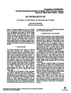
INSTITUTE OF PHYSICS PUBLISHING
JOURNAL OF MICROMECHANICS AND MICROENGINEERING
J. Micromech. Microeng. 12 (2002) 297–306
PII: S0960-1317(02)27886-9
Fabrication of MEMS devices by using anhydrous HF gas-phase etching with alcoholic vapor Won Ick Jang, Chang Auck Choi, Myung Lae Lee, Chi Hoon Jun and Youn Tae Kim Microsystem Team, Basic Research Laboratory, Electronics and Telecommunications Research Institute, Yuseong, PO Box 106, Daejeon 305-600, Korea
Received 15 August 2001, in final form 22 March 2002 Published 22 April 2002 Online at stacks.iop.org/JMM/12/297 Abstract In silicon surface micromachining, anhydrous HF GPE process was verified as a very effective method for the dry release of microstructures. The developed gas-phase etching (GPE) process with anhydrous hydrogen fluoride (HF) gas and alcoholic vapor such as methanol, isopropyl alcohol (IPA) was characterized and its selective etching properties were discussed. The structural layers are P-doped multi-stacked polysilicon and silicon-on-insulator (SOI) substrates and sacrificial layers are tetraethylorthosilicate (TEOS), low-temperature oxide (LTO), plasma enhanced chemical vapor deposition (PECVD) oxide, phosphosilicate glass (PSG) and thermal oxides on silicon nitride or polysilicon substrates. We successfully fabricated and characterized micro electro mechanical system (MEMS) devices with no virtually process-induced stiction and no residues. The characteristics of the MEMS devices for microsensor and microactuator, microfluidic elements and optical MEMS application were evaluated by experiment. (Some figures in this article are in colour only in the electronic version)
1. Introduction The surface micromachining process is the basis for the fabrication of micro electro mechanical system (MEMS). One of the key processes in surface micromachining is the dry release of microstructures without subsequent sticking of these structures to the substrate. Fabrication of the free microstructures is very important in micromachining to produce well-operated microsensors and microactuators. The free parts stick to an adjacent surface either after sacrificial removal or in operation. This failure process consists of temporary deformation due to capillary force during drying. The major causes of permanent stiction to an adjacent surface is the surface tension at the interface between liquid and air during drying process followed by the wet etching of the sacrificial layer [1, 2]. In the future generations of microstructures, surface tension forces will become more of a problem as these structures become longer and thinner with closer spacing. In the past, various techniques have been 0960-1317/02/030297+10$30.00 © 2002 IOP Publishing Ltd
developed to alleviate or remove the stiction problem. One is a method of undergoing an NH4F process for the silicon so as to be hydrophobic [3], and reducing the contact area between adjacent surfaces by introducing dimples [4] or by increasing surface roughness to alleviate the surface tension energy [5]. However, occasionally, residues still remain at the interface between films and at the edge of the microstructures due to chemical reaction and water condensation. As shown in figure 1, the other is a promising technique of avoiding the formation of a liquid–vapor interface by sublimation (path A → B) using p-dichlorobenzene [6] or t-butyl alcohol [7] and by supercritical transition (path A → C) of a fluid [8]. The supercritical CO2 drying method utilizes the characteristics of phase transfer to a supercritical fluid, which is an intermediate state between gas and liquid. The sublimation method directly solidifies the cleansing solution by using sublime materials. These methods show excellent results, but still require a complicated apparatus of high pressure or careful handling of the samples. But, a demand is still raised to develop a method
Printed in the UK
297
W I Jang et al pressure
anhydrous HF gas
MFC MFC
supercritical CO2 drying
etch chamber pressure gauge
nitrogen
baffle
MFC
needle valve
supercritical point
sublimation
Liquid
load/lock
shower head throttle valve heating area
Solid
wafer
Vapor
alcoholic bubbler
C
A
mass spectrometer (RGA)
D
dry pump
(a)
gas-phase etching B temperature
Figure 1. Phase diagram of dry release process in surface micromachining.
etch chamber
gas delivery box
controller for effectively and reliably releasing the microstructure with a simple drying process. Recently, anhydrous HF GPE process (path A → D) was newly developed for the release of sacrificial oxide, which is an intermediate layer between a substrate and a microstructure [9]. However, severe condensation can occur in the hydrogen fluoride (HF) etch process containing water vapor and may result in a shorter detachment length. A capillary force is generated by surface tension. If the capillary force becomes greater than the retrieving force, the microstructure tentatively sticks on the substrate. A tentative sticking is changed into a permanent surface sticking due to the van der Waals force, electrostatic force and hydrogen bridging [10]. Such a phenomenon is referred to as a stiction. In order to minimize the capillary force of the gas–liquid interface, IPA of low vapor pressure and low surface tension is employed as a catalyst instead of water vapor. The sacrificial oxide etching using anhydrous HF gas and alcoholic vapor in the gas-phase region promises to be some effective technology to avoid stiction. In this study, we introduced the gas-phase etching (GPE) process to prevent excessive condensation of water, which is generated during sacrificial oxide etching. We obtained good results by controlling the temperature and pressure of an etch chamber to be in a vapor region of a phase equilibrium diagram of water and by heating the chamber and gas lines to prevent from condensing vapors during the process. The silicon microstructures for MEMS device are completely released and fabricated by the silicon surface micromachining. We characterized the GPE process with anhydrous HF and alcoholic vapor such as methanol and IPA for the fabrication of MEMS devices and discussed selective etching properties of sacrificial oxides. We successfully fabricated and characterized MEMS devices with no virtually process-induced stiction and no residues. The characteristics of microgyroscope and electrostatic microactuator for microsensor and microactuator, thermally driven micropump for microfluidic elements, and optical switch for an optical crossconnect (OXC) router were also evaluated by experiment. 298
load/lock mass spectrometer
(b)
Figure 2. A schematic (a) and photograph (b) of the GPE system.
2. Gas-phase etching 2.1. GPE system A schematic and photograph of a GPE system are shown in figure 2. The GPE system consists of an etch chamber, a gas delivery system, vacuum exhaust, mass spectrometer and main controller. The etch chamber is made of aluminum and coated by Teflon film for anti-corrosion. Anhydrous HF (99.9% pure), methanol (99.9% pure) and IPA (99.5% pure) are delivered to the chamber through a shower head and a baffle for uniform gas distribution and flow down vertically in the chamber. The chamber wall is heated to prevent condensation of reactants. We also can minimize the condensation level by heating those parts delineated by thick lines. To prevent condensation in the gas line, the bubbler and solvent vapor delivery line are also heated to above 90 ◦ C and HF gas cylinder to 30 ◦ C. The gas delivery system is very important because the flow rates of HF gas and IPA vapor affect the characteristics of etching performance seriously. The flow rate of the anhydrous HF is controlled by a mass flow controller (MFC), and the flow rates of methanol or IPA vapor are controlled by injecting carrier gas of nitrogen into an alcoholic bubbler. The control variables of vapor flow rate are flow rates of nitrogen gas, temperature and pressure in the bubbler. The alcoholic bubbler is heated resistively, and a needle valve controls the pressure of the bubbler. This throttle valve controls the process pressures in conjunction with a capacitance manometer. The GPE conditions were a process pressure of 50 Torr, a
Fabrication of MEMS devices by using anhydrous HF gas-phase etching with alcoholic vapor
wafer temperature of 35 ◦ C and an initial vapor pressure in the methanol bubbler of 10 psi at a nitrogen flow rate of 300 sccm, or in the IPA bubbler of 10 psi at nitrogen flow rate of 1000 sccm. The flow rates of the HF gas and nitrogen gas were 100 sccm. The etching condition was a HF partial pressure of 15 Torr and a CH3OH partial pressure of 4.5 Torr. These process conditions are selected to control condensation of reactants on the etched surfaces. The dry pump is used to protect the aluminum chamber against corrosive gases. A quadrupole mass spectrometer (Hiden, model HAL/3F) can analyze the gases in the exhaust line quantitatively and allows us to observe the by-products during the etching process. And main controller integrates these modules through digital and analog interfaces according to SEMI MESC standard. This process features simplicity, virtually no capillary forces, negligible residues and even compatibility to a cluster tool for process integrating in the future [11]. This process further has an economic merit of massive production as in the case of a MEMS device. Under the temperature below the boiling point of alcohol (methanol: 64.5 ◦ C, IPA: 82.7 ◦ C), HF gas or alcohol vapor fails to arrive at the etching chamber but is partially condensed on an inner wall of a gas line or an absolute liquid column is formed along the inner wall of the gas line later, thereby failing to precisely control the amount of liquid. Therefore, maintaining the temperature to be above 90 ◦ C is to prevent such a phenomenon. The etch chamber is also heated by a heater so as not to condense the water generated in the reaction chamber. The water is completely vaporized without being condensed on the substrate by heating the entire etching chamber and gas lines during the process. 2.2. Etching mechanism and properties Oxide etching with a gas mixture of an anhydrous HF and alcoholic vapor has been modeled and characterized [12]. It has been recognized that etching in the gas-phase region takes place via a slow gas–solid reaction that is catalyzed by the adsorbed moisture on the oxide surface. A reaction between the HF gas and methanol or IPA results in H2O due to a chemical reaction. The presence of H2O on silicon oxide surfaces initiates ionization of the HF molecules, and silicon oxide reacts with the generated HF2− ion, which leads to the generation of more H2O. The generated H2O enhances the ionization reaction of HF molecules, resulting in an increase of HF2− ions. The absorbed HF2− is the most significant reactant in the gas-phase etching of sacrificial oxide just as in the liquid-phase etching. We can figure out that lower water concentration and higher HF partial pressure are preferable for the release process with reduced stiction problem. The alcohol such as methanol or IPA would help GPE to proceed with smaller water condensation because it is highly volatile and tends to evaporate easily with water. We see that it successively evaporates water in vacuum state of 50 Torr. The use of alcoholic vapor is employed as a catalyst instead of water vapor and results in the removal of other reaction products from the surface as well. The following is a chemical reaction formula representing the etching process of the silicon oxide. During the etching,
the gas molecules adsorb physically onto the silicon oxide surface as follows: HF(g) ↔ HF(ads) M(g) ↔ M(ads), (M = CH3 OH or CH3 CHOHCH3 ). The ionization reaction between the adsorbed HF and the adsorbed CH3OH results in HF2−: 2HF(ads) + M(ads) → HF2 − (ads) + MH+ (ads).
(1)
The ionized HF then reacts with the oxide by sequential substitutions of the oxygen atoms in SiO2 for the fluorine atoms in HF2−. The overall chemical reaction for undoped silicon oxide, therefore, becomes SiO2 (s) + 2HF2 − (ads) + 2MH+ (ads) → SiF4 (ads) + 2H2 O(ads) + 2M(ads).
(2)
SiF4 (ads) ↔ SiF4 (g) H2 O(ads) ↔ H2 O(g) M(ads) ↔ M(g). Finally, the by-products of SiF4, CH3OH and H2O in equation (2) are removed from the oxide surface by desorption during heating. The presence of CH3OH on the silicon oxide surface initiates ionization of the HF molecules, and the silicon oxide reacts with the HF2− ions, which leads to more generation of H2O, as shown in equation (2). The etch rate and the selectivity for the GPE were affected by the amounts of HF and CH3OH adsorbed physically on the oxide surface. The oxide etch rate is expected to be proportional to the ionization reaction rate and, thus, dependent on the partial pressures of HF and CH3OH and wafer temperature inside the reaction chamber. In the meantime, we performed the GPE process at 50 Torr and 35 ◦ C for an effective removal of water using thermodynamic properties of H2O. We need to maintain a high flow rate of HF gas and low process pressure for minimization of condensation on the sacrificial oxide. The alcohol replace water in the roles of etch initiator and mediator. The advantages associated with alcohol stem from the ability to control the water by-product concentration in the condensed surface reacting layer. By eliminating water from the oxide surface, alcohol continuously remove the least volatile species in the etch reaction, and the surface condensed layer is controlled to minimal thickness. In [13], water, an etch product, has the lowest vapor pressure, followed by IPA, ethanol, methanol and anhydrous HF. Specifically, methanol is expected to enhance the removal of native oxide in cleaning technology. Since IPA has the lowest vapor pressure among these alcohol, it is expected to encompass a wide range of etch rates for sacrificial oxide removal in surface micromachining. To prevent water condensation during the GPE process, we could either reduce the process pressure or increase the temperature in the phase diagram for water. Figure 3(a) shows the temperature dependence of the empirical etch rates for the bulk TEOS oxide. The etching rate was reduced gradually as a wafer temperature increased. This is due to the reactant species absorbed on the oxide surface decreasing with increasing temperature. Both for the bulk and the sacrificial TEOS oxides, the process condition at 35 ◦ C showed half the etch rate compared to that of a previous process at room temperature. 299
W I Jang et al 250
TEOS (0.1-2um)
Poly-Si (2um)
Etch Rate (nm/min)
200
150
PHF =11.4 torr, PM /PHF =0.17 PHF =5.9 torr, PM /PHF =0.66 M=CH3OH
100
Etched oxide length
50
0
20
30
40
50
60
70
θ
80
Etched profile
o
Wafer Temperature ( C)
TEOS
(a)
LTO TEOS OXIDE PECVD OXIDE PSG
3
(a) 80 TEOS thickness
70
2
1 0
200
400
600
800
1000
1200
1400
1600
1800
2000
Etching Time (sec) (b)
Figure 3. Etch rate (a) versus temperature for AHF/methanol GPE of TEOS oxide and etched thickness and (b) versus time for AHF/IPA GPE of sacrificial oxides.
Etched oxide length (µm)
Etched Thickness (µm)
4
0.1µm 0.5µm 1.0µm 2.0µm
60 50 40 30 20 10 0 0
500
1000
1500
2000
2500
3000
3500
Etching time (s)
And the etch rate may be lowered or enhanced by either controlling the partial pressure of the anhydrous HF gas or varying the kinds and partial pressures of alcoholic vapor. Figure 3(b) shows etched thickness as a function of etching time for various oxides. LTO, TEOS oxide and PECVD oxide of about 3.3 µm thickness, and PSG of about 2.3 µm thickness were used as a sacrificial layer. At 35 ◦ C and 50 Torr, the etch ˚ min−1 rates of the AHF/methanol GPE were about 400 A ˚ min−1 for LTO and 55 A ˚ min−1 for for TEOS oxide, 200 A thermal oxide. The etch rate of PSG is higher than that of the other oxides because the adsorption of reactant species on the PSG surface is much larger than that on other oxides [9, 12]. The etch rate of AHF/IPA GPE is seven times as fast as that of AHF/methanol GPE. Figure 4(a) shows crosssectional views for measuring the etched oxide length in onedimensional (1D) microchannel of polysilicon cantilevers. In the steady state, we can see that the etched angle (θ ) between the bottom of the upper polysilicon and the etched profile of the TEOS became about 60o, regardless of the TEOS thickness. Although we expected that the etch rate for the sacrificial TEOS might depend on the height of the microchannel, not so much difference could be noticed for the range of 0.1–2 µm, 300
(b)
Figure 4. SEM photograph (a) of the fabricated polysilicon cantilevers and the lateral etching speed (b) in 1D microchannel after AHF/methanol GPE.
as shown in figure 4(b). We believe that there is no severe depletion region of the HF etchant in 1D microchannel at this condition. Also the GPE showed a lateral etching speed of 1.24 µm min−1 for a 2.0 µm thick TEOS and 0.02 µm min−1 for a 1.8 µm thick thermal oxide in 1D microchannel. The silicon oxide undergoing a removal process meets evaporating water drops, thereby leaving diverse kinds of residues that are not evaporated on the substrate due to condensation. Stiction occurs and residues remain on the incompletely etched silicon oxide because of a scum, side wall polymerization and decorations of HF, and so on. It is well known that H3PO4 is formed during etching of PSG in HF solution, in which the bonding state of the phosphorus atoms in the liquid is mainly PO43– [14]. A H3PO4 is generated in the reaction of H2O with P2O5, the bonding state of phosphorus in PSG film. Here, as shown in equation (2), H2O is formed
Fabrication of MEMS devices by using anhydrous HF gas-phase etching with alcoholic vapor
(a)
(b)
(c)
(d)
Figure 5. SEM photographs of TEOS oxide (a), PSG (b), LTO (c) on the nitride and TEOS oxide (d ) on the polysilicon.
in the reaction of HF with SiO2, the bonding state of silicon in PSG film. The water serves as a catalyst for the reaction of HF with the oxide. The H3PO4 is highly hygroscopic and, therefore, readily absorbs the water molecules generated in the continuing reaction of HF with SiO2, and H3PO4(H2O) is generated. P2 O5 (s) + 3H2 O(ads) → 2H3 PO4 (ads)
(3)
H3 PO4 (ads) + H2 O(ads) → H3 PO4 (H2 O)(ads)
(4)
−
2HF(ads) + H2 O(ads) → HF2 (ads) + H3 O (ads). +
(5)
Therefore, the following etching reaction of PSG is proposed: 2SiO2 (s) + P2 O5 (s) + 4HF2 − (ads) + 4MH+ (ads) → 2SiF4 (ads) + 2H3 PO4 (H2 O)(ads) + 4M(ads).
(6)
SiF4 (ads) ↔ SiF4 (g) M(ads) ↔ M(g). The characterization analysis of residues was carried out by using scanning electron microscopy (SEM) and auger electron spectroscopy (AES). Figure 5 shows SEM photographs of TEOS oxide (a), PSG (b), LTO (c) on the nitride and TEOS oxide on the polysilicon (d). As shown in
figures 5(a) and (b), scratch-shaped SiOxNy, and mushroomshaped or island-shaped SiOxNy layers are detected on the nitride surface after the GPE of TEOS and LTO, respectively. After the GPE of TEOS or LTO, residues were detected on the nitride substrate, as shown in figure 6 of AES depth profiles. The composition of the residue in figure 5(a) was observed because of nitride compound, which is generated at the interface between the nitride and oxide substrates during etching. The surface of the silicon nitride is changed and oxidized after this material is exposed to a wet oxygen ambient during etching. The AHF GPE etched the oxidized surface in a slow, nonuniform fashion [15]. As a result, the composition of the residues changes from stoichiometic SiO2 to SiOxNy near the nitride interface. As shown in figure 5(c), residues of the bubble-shaped H3PO4(H2O) have been observed after the etching of PSG on the nitride substrate. After the GPE of TEOS, LTO and PSG on the nitride substrate, the polysilicon microstructures are stuck to the underlying substrate because neither the SiOxNy layers nor the H3PO4(H2O) layer vaporize. The bubble-shaped H3PO4(H2O) is formed as a liquid state, as described in equation (6). Thus, this layer does not vaporize at process pressure. We found that the etching of TEOS, LTO and thermal oxide on a polysilicon substrate shows no residue and no stiction. 301
W I Jang et al
NO
Si
Si N O ( ) Figure 6. AES spectrum and depth profiles for residues after AHF/methanol GPE of LTO on the nitride substrate.
silicon
sacrificial oxide
metal
substrate (a)
mask (d )
anchor (b)
structural layer (e)
(c)
Figure 7. Generalized process sequence for the fabrication of MEMS device. (a) silicon on insulator, (b) patterning of etch-mask, (c) patterning by (Deep) RIE, (d ) patterning of metal pads and (e) AHF gas-phase etching.
3. Fabrication of MEMS device Figure 7 shows generalized process sequences for the fabrication of various actuators in MEMS devices. A 5 inch (100) silicon wafer or SOI wafer was used as a substrate for the microstructure pattern. After standard cleaning in wet station of 4:1 H2SO4/H2O2 and 100:1 HF solution, thermal oxide was deposited by oxidation of 1000 ◦ C in H2/O2 ambient. Silicon nitride was deposited by LPCVD (low pressure chemical vapor deposition) process at 800 ◦ C and 290 mTorr using SiH2Cl2 and NH3. Sacrificial layers are TEOS, LTO, PECVD oxide, PSG and thermal oxides on silicon nitride or polysilicon substrates. TEOS oxide was deposited by LPCVD process at 710 ◦ C and 350 mTorr using TEOS and N2 . LTO was deposited 302
Figure 8. Overall view of the fabricated microgyroscope.
in a LPCVD reactor at 420 ◦ C and 240 mTorr using SiH4 and O2. PECVD oxide was deposited by LPCVD process at 400 ◦ C and 3 Torr using SiH4 and N2O. And PSG film was deposited by APCVD process at 375 ◦ C using SiH4, PH3, N2 and O2. The structural layers are multi-stacked polysilicon and SOI substrates. The polysilicon is then deposited in an LPCVD reactor at 625 ◦ C and 280 mTorr using SiH4 and is doped by a POCl3 diffusion process at 900 ◦ C during 30 min. And photoresist, TEOS or LTO is used as a masking layer. The structural layer was patterned by conventional optical lithography using a g-line wafer stepper (Nikon, NSR1505G3A) and etched by successive RIE process [16]. Multi-layered polysilicon film is annealed in nitrogen at 1000 ◦ C for 1 h to relieve the residual stress and the internal stress gradient [17]. Metal layer of Al-1% Si is sputtered and patterned. Alloy process is finished by the annealing process of 400 ◦ C in N2/H2 ambient. The newly developed anhydrous HF GPE with alcoholic vapor has been employed to release various microstructures. To reduce the etching time, we adopted a two-step process of the GPE after 6:1 BHF wet etch for the removal of a thermal oxide. The silicon microstructures for the fabrication of MEMS device were finally released from the underlying substrate by the GPE of the sacrificial oxide. 3.1. Microgyroscope A 5 inch p-type (100) silicon wafer with a resistivity of 5–8 � cm was used as the substrate for the microstructure pattern. After thermal oxidation (0.2–0.3 µm), nitride or polysilicon (0.1–0.3 µm) were deposited on silicon wafers by the LPCVD process. And TEOS, LTO and PSG films (1.5–3 µm) are uniformly deposited as sacrificial layers. LPCVD multi-stacked polysilicon (2–6.5 µm) is deposited as a structural layer. And TEOS and LTO are deposited as (0.1–2 µm) sacrificial layers and (0.8–1.2 µm) masking layers. The fabricated microgyroscope using the silicon-oninsulator structure and its schematic are shown in figure 8. The microgyroscope was designed to vibrate in two perpendicular axes on the substrate plane. The gyroscope consists of two shuttle masses, eight folded springs, a pair of
Fabrication of MEMS devices by using anhydrous HF gas-phase etching with alcoholic vapor
sensing electrodes, driving electrode and driving monitoring electrode. The fabricated microgyroscope was tested under the operating condition of dc 4 V, ac 0.1 V, in a vacuum chamber of 100 mTorr. The detection circuit consists of a discrete sense amplifier and a noise canceling circuit. By adjusting the dc voltage slightly, the sensing resonant frequency can be tuned to the driving resonant frequency. 3.2. Electrostatic microactuator
3.3. Thermally driven micropump A thermally driven micropump for fluid has been designed and fabricated by surface micromachining, as shown in figures 10(a)–(c). A 5 inch p-type (100) silicon wafer with resistivity of 1–30 � cm was used as a substrate. After standard ˚ and silicon nitride (3000 A) ˚ cleaning, thermal oxide (3000 A) layers were deposited on the substrate by thermal oxidation and ˚ of bottom the LPCVD process. And then polysilicon (8000 A) ˚ of sacrificial oxide were deposited heater and LTO (2000 A)
(a)
(b)
0.6
Maximum Deflection (µm)
A 5 inch p-type (100) silicon wafer was also used as the substrate for the microactuators pattern. After thermal ˚ polysilicon (4000 A) ˚ on silicon wafers oxidation (3000 A), are deposited by the LPCVD process and doped by a POCl3 diffusion process at 900 ◦ C during 30 min. A 0.8–2 µm thick sacrificial layer of LTO is deposited in a LPCVD reactor at 420 ◦ C. This layer is then dry etched down to the substrate, using mask 1, to open the anchor areas for the polysilicon beams. Doped polysilicon of 0.7–2 µm thickness is then deposited in an LPCVD reactor at 625 ◦ C. This layer is annealed in nitrogen at 1000 ◦ C for 1 h to relieve the internal stress and the stress gradient of a multi-layered polysilicon film. The micropump actuation structures are then defined in this layer with mask 2 by RIE of polysilicon. A twomask fabrication process was used to prepare the micropump structures. Diaphragm structures of 110 µm diameter are cantilever-type polysilicon. Static deflection with uniformly distributed load of q = −ε0 V 2 /d 2 is δ = (qx/24EI )(L3 − 2Lx 2 + x 3 ) for a clamped-free beam such as cantilever type, where ε0, x, L, a and r are permittivity in vacuum, distance from fixed wall, length of beam, radius of circular plate and distance from the plate’s center, respectively. Laser displacement meter (Keyence Model LT-8010) is used to measure the diaphragm deflection of the micropump by an electrostatic force. The natural frequency of microstructure beam such � �for single-span � as cantilever or bridge is fi = λ2i 2πL2 (EI /m)1/2 . Then λi = 1.875 104 07 for cantilever type and λi = 4.730 040 74 for bridge type. Here L, E, I and m are length, area, moment of inertia and mass per unit length of beam, respectively. A polysilicon diaphragm for a micropump has been designed and fabricated by surface micromachining, as shown in figures 9(a) and (b). We successfully fabricated micropump actuators with no virtually process-induced stiction and no residual products after GPE of LTO on polysilicon substrates. Figure 9(c) represents the experimental static deflection of the micropump actuators. Finally, the cantilever-type micropump actuators move at 5 V and 1 Hz and operate at square wave voltage of 10 V and 2 Hz for air under near room temperature and normal atmospheric pressure.
0.5 0.4 0.3 0.2 0.1 0.0 0
3
6
9
12
Voltage (DC V) (c)
Figure 9. The overall view (a) and its enlarged view (b), and static displacement (c) of the cantilever-type microactuators.
and patterned after n+ doping with POCl3 diffusion at 900 ◦ C for 30 min. After annealing at 1000 ◦ C for 1 h, polysilicon ˚ layer was subsequently deposited by LPCVD and the (2000 A) heater area opened by RIE. PECVD oxide of 6 µm thickness was deposited as a sacrificial layer and corrugated with 2 µm thickness for these oxides. Polysilicon membrane of 2 µm thickness is deposited in a LPCVD reactor at 650 ◦ C and 200 mTorr using SiH4. The etch holes of 1 µm diameter with 5 µm distance on the membrane of 2000 µm diameter were opened by successive RIE. Metal layer of Al-1% Si (1.0 µm) is sputtered and patterned. Alloy process is finished by the annealing process of 400 ◦ C in N2/H2 ambient. Anhydrous HF/IPA GPE of PECVD oxide has been developed to remove oxides and release the membrane through the etch holes. To remove thick oxides in silicon surface micromachining, the AHF GPE with IPA vapor was verified as a very useful method for the dry release of microstructures. The surface micromachined membrane is coated by positive photoresist ˚ or AZ1512 of 2 µm) at 4000 rpm, (TSMR GA-2 of 7000 A followed by soft bake at 90 ◦ C for 90 s on a hot plate and hard bake at 120 ◦ C for 10 min in a convection oven. Finally, the surface micromachined micropump is packaged with a glass microchannel of 20 µm depth and 2500 µm width. Each pumping chamber is symmetric and 6 µm deep, as shown in figure 10(d). 303
W I Jang et al
2000 µ m
membrane
(b)
inlet port
(c)
three membranes
outlet port
metal pads
diffuser valve
electrodes nozzle valve (d)
(a)
µm) Displacement (µ
80 60 40 20 0
0
5
10
15
20
25
30
35
Voltage (V) (e)
Figure 10. Overall view (a), opened and buried heaters (b) and (c), packaged microchannel (d ) and experimental center displacement (e) of thermally driven micropump.
We successfully fabricated surface micromachined micropump with no virtually process-induced stiction and no residues. The thermally driven micropump for air operates in the range of 10–30 V under near room temperature and normal atmospheric pressure. Laser displacement meter is also used to measure the membrane deflection of the micropump by a thermoelastic force. Maximum center deflection for air is about 63.5 µm at square wave of 30 V and 1 Hz. The divergence angles of diffuser and nozzle valves are about 10◦ , the inlet and outlet diameters of Tygon tube are 0.51 mm and 1.52 mm, respectively. The heaters with a resistance of 100– 500 � were released in the cavity to minimize heat conduction to the substrate. The actuators were operated with three phase sequence by driving circuit. 3.4. Thermoelastic microactuator Optical switches for an OXC are expected to become essential components in wavelength division multiplexer (WDM) optical communications [18]. Latch-up actuation is prerequisite to implement an optical switch with low power consumption and high reliability. Fang and Wickert [19] investigated on the buckling behavior of micromachined clamped–clamped beams (bridge structure), but which have no initial rise and cannot be directly utilized in the microactuator with bi-stable operation. To design a surface micromachined latch-up type optical switch, microactuator should have a 304
bi-stable characteristic. One of the approaches to bi-stability is that the microactuator should have a buckling operation, which can be easily implemented by shallow arch-shaped leaf springs. We proposed a planar thermoelastic microactuator with a latch-up operation for optical switching. We designed and fabricated a thermoelastic microactuator for 2 × 2 micro opto electro mechanical (MOEM) optical switch for telecommunications networks. The proposed microactuator consists of four cantilever-shaped thermoeleastic actuators (12 µm width, 600 µm length), four levers (12 µm width, 300 µm length) for displacement expansion, two shallow arch-shaped leaf springs (3 µm width, 600 µm length), a mobile shuttle mass with a vertical micromirror and four elastic boundaries, all of which are located in the substrate plane, as shown in figure 11(a). Fabrication uses only a single mask. It starts with a photolithography on SOI wafers with sacrificial oxides of 2 µm thickness to define microstructures. As an etch mask, photoresist of 1.4 µm thickness was deposited and patterned. The height of the device layer is 45 µm, which is sufficient to cover well the fiber core. The spot diameter of single mode fibers is typically 10 µm. Without RIE lag or microloading effect [20], the device layer was etched using inductively coupled plasma (ICP) for Si Deep RIE. The verticality was almost 90◦ , the size of scallop is about 80 nm. For an increased reflectivity the silicon mirrors are coated with aluminum. Their reflectivity was calculated to be 95.4%. This is done by e-beam evaporation, where the
Fabrication of MEMS devices by using anhydrous HF gas-phase etching with alcoholic vapor
700µ µ µm
ANCHOR
VERTICAL MIRROR
LEVER(C)
SHUTTLE MASS
LEVER
700µm µ
THERMOELASTIC ACTUATOR
CLAMPED HINGE (B)
BUCKLING SPRING ELASTIC BOUNDARY
THERMOELASTIC ACTUATOR (A)
ANCHORS
(a)
(b)
PROBES
LEVER THERMOELASTIC ACTUATOR
Displacement ( µ m)
ANCHOR
30
1Hz 10Hz 50Hz simulation
25
20
15
10
5
0 0
2
4
6
8
10
12
Applied Voltage (V)
(c)
(d)
Figure 11. Overall view (a), simulated temperature profile (b), heating state (c) and displacement profile of the thermoelastic microactuator for comparison between simulated and measured results (d ).
wafers are oriented in an appropriate directions. Finally, the sacrificial oxide is removed by anhydrous HF GPE process for the release of microstructures free of stiction. The actuation is incurred by the thermal expansion due to the current flow in the active cantilevers and the linear expansion of the microactuator is mechanically amplified by lever mechanism, and transferred to the shuttle mass for the movement of vertical micromirror. When an input voltage is applied to two electrodes of 5 V potential, maximum temperature, in figure 11(b) simulated ANSYS 5.6, is about 436 ◦ C. Then the lengths of the microacuator (A), clamped hinge (B) and lever (C) are 500 µm, 20 µm and 260 µm, respectively. The thickness of structures is 2 µm. Figure 11(c) shows heating state of the microactuator on applied voltage. The experimental and simulated displacements of the prototype microactuator according to applied voltages are shown in figure 11(d). The microactuator showed the simulated displacement of 21 µm at 10 V of input voltage. The experimental and simulated displacements are proportional to 1.5 times of power and square of input voltage. The
experimental displacement amplified by the microactuator of 600 µm length and lever of 300 µm length was more than 30 µm at 20 V input voltage. The frequency response for square wave input was measured up to 90 Hz. Latch-up operation is realized by using shallow arch-shaped buckling springs, thermoelastic actuators with displacement magnifying leverages. Then driving voltage in the forward moving is about 23 V, but in the backward moving is about 15 V because of the restoring force of buckling springs. The switching time from settling characteristics of the thermoelastic microactuator is below 5 ms. After 1 530 000 cycles for 17 h at 25 Hz, the aging of the microactuator begins to appear by an oxidation in the atmospheric conditions without fracture of the hinge.
4. Conclusion The GPE with anhydrous HF gas and alcoholic vapor was introduced and verified as a very effective method for the dry release of microstructures. The developed GPE process 305
W I Jang et al
with anhydrous HF gas and alcoholic vapor was characterized and its selective etching properties were discussed. We successfully designed and fabricated MEMS devices with no virtually process-induced stiction and no residues after the GPE of sacrificial oxides on polysilicon substrates. The proposed process features simplicity, virtually no capillary forces and compatibility with conventional IC processes as well.
Acknowledgments The authors would like to thank the members of semiconductor laboratory for their experimental contribution and special thanks to Prof M Esashi at NICHe in Tohoku University for his technical discussion. This research work is supported financially by the Ministry of Information and Communications, Korea.
References [1] Legtenberg R, Elders J and Elwenspoek M 1993 Stiction of surface micromachined structures after rinsing and drying: model and investigation of adhesion mechanisms Int. Conf. on Solid-State Sensors and Actuators (Transducers 93) (Yokohama, 1993) pp 198–201 [2] Mastrangelo C H and Hsu C H 1993 Mechanical stability and adhesion of microstructures under capillary forces:I. Basic theory J. MEMS 2 33–43 [3] Houston M R, Madoudian R and Howe R T 1995 Ammonium fluoride anti-stiction treatments for polysilicon microstructures Int. Conf. Solid-State Sensors and Actuators (1995) pp 210–3 [4] Kim C-J, Pisano A P, Muller R S and Lim M G 1990 Polysilicon microgripper IEEE Solid-State Sensor and Actuator Workshop (Hilton Head Island, SC, June 1990) pp 48–51 [5] Yee Y, Chun K, Lee J D and Kim C-J 1996 Polysilicon surface modification technique to reduced sticking of microstructures Sensors Actuators A 52 145–50 [6] Guckel H, Snielgowski J J and Christenson T R 1989 Advances in processing techniques for silicon micromechanical devices with smooth surfaces Proc. IEEE Micro Electro Mechanical Systems (Salt Lake City 1989) 71–5
306
[7] Ohtsu M, Minami K and Esashi M 1996 Fabrication of packaged thin beam structures by an improved drying method Proc. IEEE Micro Electro Mechanical Systems (San Diego 1996) 228–33 [8] Mulhern G T, Soane D S and Howe R T 1993 Supercritical carbon dioxide drying of microstructures Int. Conf. on Solid-State Sensors and Actuators (Transducers ’93) (Yokohama, 1993) pp 296–9 [9] Lee J H, Jang W I, Lee C S, Lee Y I, Choi C A, Baek J T and Yoo H J 1998 Characterization of anhydrous HF gas-phase etching with CH3OH for sacrificial oxide removal Sensors Actuators A 64 27–32 [10] Maboudian R and Howe R T 1997 Critical review: adhesion in surface micromechanical structures J. Vac. Sci. Technol. B 15 pp 1–20 [11] Lee J H, Jang W I, Choi B Y, Yoo H J and Park S-C 1995 Development of a MESC-compliant cluster tool Solid State Technol. 38 93–7 [12] Lee C S, Woo S I, Baek J T, Yoo H J and Woo S I 1996 Modeling and characterization of gas-phase etching of thermal oxide and TEOS using anhydrous HF gas and CH3OH vapor J. Electrochem. Soc. 143 1099–103 [13] Torek K, Ruzyllo J, Grant R and Novak R 1995 Reduced pressure etching of thermal oxides in anhydrous HF/alcoholic gas mixtures J. Electrochem. Soc. 142 1322–6 [14] Tong J E, Schertenleib K and Carpio R A 1984 Process and film characterization of PECVD borophosphosilicate films for VLSI applications Solid State Technol. 27 161–70 [15] Loewenstein L M and Tipton C M 1991 Chemical etching of thermally oxidized silicon nitride: comparison of wet and dry etching methods J. Electrochem. Soc. 138 1389–94 [16] Park H H, Kwon K H, Lee S H, Koak B H, Nahm S, Lee H T, Cho K I, Kwon O J and Kang Y I 1994 A study on modified silicon surface after CHF3/C2F6 reactive ion etching ETRI J. 16 45–57 [17] Choi C A, Lee C S, Jang W I, Hong Y S, Lee J H and Shon B K 1999 Stress characteristics of multi-layered polysilicon film for the fabrication of microresonators Japan. J. Appl. Phys. 38 3693–9 [18] Walker J A 2000 The future of MEMS in telecommunications networks J. Micromech. Microeng. 10 R1–R7 [19] Fang W and Wickert J 1994 Post-buckling of micromachined beams 99 IEEE Workshop on MEMS (Microelectromechanical Systems) pp 182–7 [20] Jansen H, be Boer M and Elwenspoek M 1996 The black silicon method IV: high aspect ratio trench etching for MEMS applications Proc. IEEE Workshop on MEMS ’96 (San Diego, Feb. 1996) pp 250–7