ATHENA framework is used to design the 2D solar cell structure with area 50Ã10 µm2. Then the voltage was applied on device by using ATLAS framework to.
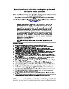
American Journal of Applied Sciences 6 (12): 2043-2049, 2009 ISSN 1546-9239 © 2009 Science Publications
Fabrication of Single Layer SiO2 and Si3N4 as Antireflection Coating on Silicon Solar Cell Using Silvaco Software 1
A. Lennie, 1H. Abdullah, 2S. Shaari and 3K.Sopian Department of Electrical, Electronics and Systems Engineering, Faculty of Engineering and Built Environment, University Kebangsaan Malaysia, 43600 Bangi Selangor, Malaysia 2 Laboratory of Photonics Technology, Institute of Microengineering and Nanoelectronics, University Kebangsaan Malaysia, 43600 Bangi Selangor, Malaysia 3 Solar Energy Research Institute, University Kebangsaan Malaysia, 43600 Bangi Selangor, Malaysia 1
Abstract: The main objectives was to investigate and enhance the short circuit current density, Jsc and also to improve the efficiency of silicon solar cell by fabricating a layer of silicon dioxide (SiO2) and silicon nitride (Si3N4) coatings on silicon solar cell. This fabrication carried out on high temperature during annealing process from 800-1050°C and variable thickness of antireflection coating (ARC) layer from 50-90 nm thick. The photovoltaic properties of Si3N4 layer have been compared with SiO2 layer to determine which material is suitable in fabricating single layer ARC. Solar cell simulation could be useful for time saving and cost consumption. Problem statement: The Silvaco software is not widely used in designing the 2D solar cell devices because there are lots of 1D, 2D and 3Dsimulation beside Silvaco software such as MicroTec, SCAPS-1D. Approach: The silicon dioxide (SiO2) and silicon nitride (Si3N4) coating have been modeled and fabricated on silicon solar cell by using Silvaco software packaging. Results: For SiO2 results, the FF value is approximately 0.758 and η maximum 9.43%. In annealing process, the temperature becomes higher resulted increasing of pn junction depth. However, not to Voc and Jsc values, both parameters were slowly decreased when temperature increased. Meanwhile, when the thickness of SiO2 layer is increased, the parameters of pn junction depth, Jsc, Voc, FF and η were decreased slowly. As for Si3N4 result, the calculated FF approximately 0.758 and η maximum is 9.57%. During annealing process, the temperature increasing constantly follows the increasing of pn junction depth and Jsc, meanwhile the Voc is decreased slowly. In variable Si3N4 thickness simulation, the output parameters of pn junction depth, Jsc, Voc, FF and η were decreased when the thickness increased 10 nm each simulation. Conclusion: The optimum temperature during annealing process for SiO2 is 950°C, while for Si3N4 is 1050°C. For the thickness analysis, the optimum ARC thickness for SiO2 and Si3N4 layer is 50 nm both. Key words: Silicon solar cell, SiO2, Si3N4, efficiency, Silvaco INTRODUCTION Traditional fuel energy resources are limited and generate harmful waste products in the atmosphere. Hence, alternative eco-friendly energy sources are receiving increasing attention. Of all substitute energy sources, solar power is most attractive because of its abundance and the consistency of sunlight[1]. In 1950s, Chapin et al.[2] at Bell laboratories developed the first crystalline silicon solar cell with a solar-energy conversion efficiency of 6%. However, the relatively
high cost of manufacturing these silicon cells has prevented them from extensive use. Moreover, another disadvantage of silicon cells is the use of toxic chemicals during manufacturing. Accordingly, the development of low-cost organic solar cells is urgent. High quality Anti-Reflective Coatings (ARC) have become a vital feature of high-efficiency silicon solar cells[3]. Several authors have conducted extensive studies in past few years to investigate the effects of various ARC on high efficiency monocrystalline and polycrystalline solar cells[4]. Several materials having
Corresponding Author: H. Abdullah, Department of Electrical, Electronics and Systems Engineering, Faculty of Engineering and Built Environment, University Kebangsaan Malaysia, 43600 Bangi Selangor, Malaysia
2043
Am. J. Applied Sci., 6 (12): 2043-2049, 2009 the appropriate refractive index have been proposed and used for single or double layer ARC, such as TiO2 (n = 2.2), MgF2 (n = 1.35), ZnS (n = 2.3), CVD SiN (n = 1.6-2.4) and SiO2 (n = 1.46). The thickness and refractive index play role in photoelectrical conversion by reducing the reflectivity losses. The refractive index of stoichiometric LPCVD Si3N4 is close to the calculated value of 2.3 for the top layer. Silvaco TCAD offers complete and well-integrated simulation software for all aspects of solar cell technology. TCAD modules required for solar cell simulation include: S-Pisces, blaze, Luminous, TFT, Device3D, Luminous3D and TFT3D[5]. S-Pisces is an advanced 2D device simulator for silicon based technologies that incorporates both drift-diffusion and energy balance transport equations. Large selections of physical models are available for solar cell simulation, which includes surface/bulk mobility, recombination, impact ionization and tunneling models. Blaze simulates 2D solar cell devices fabricated using advanced materials. It includes a library of binary, ternary and quaternary semiconductors. Blaze has builtin models for simulating state-of-the-art multi-junction solar cell devices. Luminous and Luminous3D are advanced 2D and 3D simulator specially designed to model light absorption and photogeneration in nonplanar solar cell devices. Exact solutions for general optical sources are obtained using geometric ray tracing. This feature enables Luminous and Luminous3D to account for arbitrary topologies, internal and external reflections and refractions, polarization dependencies and dispersion. Luminous and Luminous3D also allows optical transfer matrix method analysis for coherence effects in layered devices. The beam propagation method may be used to simulate coherence effects and diffraction. The purpose of this work is to investigate and enhance the short circuit current density, Jsc and also to improve the efficiency of silicon solar cell by fabricating single layer of SiO2 and Si3N4 coatings on silicon solar cell using Silvaco TCAD software.
ATHENA framework is used to design the 2D solar cell structure with area 50×10 µm2. Then the voltage was applied on device by using ATLAS framework to compute open circuit voltage, Voc and short circuit current density, Jsc. In this simulation, the incident light has been fixed to 90° angle. The 90° incident light was applied on the top of silicon solar cell to trace the reflectance in silicon wafer (Fig. 1 and 2). In first simulation, the variable temperature that has been decided to analyze is 800, 850, 900, 950, 1000 and 1050°C. Then the second simulation, the variable thickness for this analysis is 50-90 nm with interval 10 nm thick. Table 1 show the details of input data were used in modeling solar cell structure for both analyses.
(a)
MATERIALS AND METHODS The solar cell that has been chosen for test is made in usual method in VLSI. An orientation of silicon wafer is with 50 µm thickness and boron concentration of 1×10¹⁴ atom cm−2 was chosen to create p-type silicon substrate. The p-n junction was developed by phosphorus implantation with 1×10¹⁶ atom cm−2 and energy is 30 eV. The diffuse time 60 min and temperature is variable parameter. The deposition of ARC also considered as variable parameter. The
(b)
Fig. 1: The cross-section of 10×10 µm2 solar cell structure with SiO2 single layer coating; (a) basic color region. (b) net doping color region
2044
Am. J. Applied Sci., 6 (12): 2043-2049, 2009 Table 1: Input data were used in modeling solar cell structure for SiO2 and Si3N4 simulation Parameter First simulation Second simulation Orientation 100 100 50 × 10 50 × 10 Device area (µm2) Phosphorus doping (atom m−2) 1×10¹⁶ 1×10¹⁶ Energy (eV) 30 30 Diffuse time (min) 60 60 Diffuse temperature (°C) 800, 850, 900, 950 950, 1000, 1050 ARC thickness (nm) 50 50, 60, 70, 80, 90 Incident light beam (°) 90 90
RESULTS The solar cell structure has been modeled by using Silvaco TCAD tools. The variable temperature that has been simulated in first simulation is 800, 850, 900, 950, 1000 and 1050°C. Meanwhile the variable thickness that has been fabricated in second simulation is 50, 60, 70, 80 and 90 nm. After all simulations have been done running, the Athena framework will display the 2D device structure. Figure 1 and 2 illustrated cross-section of 10×10 µm2 solar cell structure when heating in 950°C on 50 nm thick of SiO2 and Si3N4 single layer, respectively, in first simulation. In this study, the simulation only concentrated on normal incident light beam for both ARC materials. Silvaco TCAD tools can simulate the various aspects of solar cell characteristics. Typical characteristics include collection efficiency, spectral response, open circuit voltage (Voc) and short circuit current density (Jsc). Figure 3 described the electrical properties of current density-voltage (J-V) for variable temperature simulation on 50 nm SiO2 and Si3N4 layer deposited on silicon solar cell. While Fig. 4 displayed the J-V characteristics for variable thickness simulation on SiO2 and Si3N4 layer when annealing temperature was fixed to 950°C in second simulation.
(a)
(b)
Fig. 2: The cross-section of 10×10 µm2 solar cell structure with Si3N4 single layer coating
The pn junction can be seen clearly on Fig. 1a and 2a where the horizontal line under SiO2 and Si3N4 coating on silicon substrate. The distance between p-n layers DISCUSSION has been extracted using Athena simulator. The SiO2 layer has a pn junction 0.574 µm meanwhile Si3N4 layer Figure 1a and 2a shows the colors of silicon has a tiny pn junction of 0.429 µm, both are from 50 substrate region before applying net doping application nm ARC at 950°C result as shown in Table 4 and 5. In Fig. 3 and 4, the Jsc value is extracted from the command. When the 90° incident light was applied on curve when voltage is zero. On the other hand, the Voc device, there is no reflection beam on silicon substrate also can be extracted from the J-V curve when current region because the device surface is even. If the structure is zero. In this Fig. 4 clearly shows the current density were modified in different surface textured, the incident increased follows voltage value. In J-V curve of Si3N4 light on substrate will reflected between device walls[6]. layer, we can see the current density and voltage While the Fig. 1b and 2b shows the solar cell device values on thickness 90 nm were less compared to when applying the net doping color region. The net other thickness. In overall the range of current density, doping color under SiO2 and Si3N4 coating represents the Jsc for SiO2 layer is around 3.120-3.129 mA cm−2 and pn junction developed after phosphorus doping during + implantation process of n layer on silicon substrate. Si3N4 layer is approximately to 3.169-3.170 mA cm−2, 2045
Am. J. Applied Sci., 6 (12): 2043-2049, 2009
(a)
(a)
(b)
(b)
Fig. 3: (a) J-V curve of 50 nm SiO2 on silicon solar cell for variable temperature. (b) J-V curve of 50 nm Si3N4 on silicon solar cell for variable temperature
Fig. 4: (a) J-V curve of SiO2 layer on silicon solar cell for variable thickness. (b) J-V curve of Si3N4 layer on silicon solar cell for variable thickness
as shown in Table 2 and 3. This means the Jsc of Si3N4 layer is higher than SiO2 layer. Meanwhile the Voc of both layer are nearly to 0.40 V. In this project, the first simulation has been done running is simulation of variable temperature parameter from 800-1050°C with interval 50°C. For second simulation is variable thickness antireflective coating from 50-90 nm with interval 10 nm. Atlas simulator simulated the pn junction, Voc and Jsc, but the Fill Factor (FF) and power conversion efficiency (η) were calculated by using equations below. The fill factor, FF is the ratio of maximum power point, Pm divided by the Jsc and Voc and that is: FF =
J m ⋅ Vm Pm = J sc ⋅ Voc J sc ⋅ Voc
(1)
The fill factor is a measure of the realizable power from a solar cell. Typically, the fill factor is between 0.7 and 0.8[7]. The energy conversion efficiency of solar
Table 2: Photovoltaic properties of SiO2 on silicon solar cell with different Temperature (T) when coating layer is 50 nm pn junction T (°C) depth (µm) Voc (V) Jsc (mA cm−2) FF η (%) 800 0.4159 0.3978 3.1291 0.757 9.425 850 0.4175 0.3978 3.1290 0.757 9.425 900 0.4253 0.3978 3.1289 0.757 9.426 950 0.5742 0.3977 3.1283 0.758 9.428 1000 0.9047 0.3977 3.1262 0.758 9.426 1050 1.4309 0.3975 3.1200 0.759 9.410
cell, η is the comparison of maximum power point of cell, Pm to input light from source, Pin: η=
Pm FF ⋅ J sc ⋅ Voc × 100% = × 100% Pin Pin
(2)
Earth can received the maximum power from sun is about 1000 W m−2. So, the input power Pin is 1000 W m−2 with an air mass 1.5 (AM1.5) spectrums[8]. Table 2 and 3 show the results of photovoltaic properties that have been simulated and calculated for SiO2 and Si3N4 layers on silicon solar cell.
2046
Am. J. Applied Sci., 6 (12): 2043-2049, 2009 Table 3: Photovoltaic properties of Si3N4 on silicon solar cell with different Temperature (T) when coating layer is 50 nm pn junction T (°C) depth (µm) Voc (V) Jsc (mA cm−2) FF η (%) 800 0.3876 0.3981 3.1689 0.757 9.552 850 0.3892 0.3981 3.1689 0.757 9.552 900 0.3972 0.3981 3.1689 0.757 9.552 950 0.4290 0.3981 3.1691 0.757 9.553 1000 0.5770 0.3981 3.1695 0.758 9.558 1050 0.9944 0.3980 3.1698 0.758 9.565 Table 4: Photovoltaic properties of SiO2 on silicon solar cell with different thickness (d) when temperature is 950°C pn junction d (nm) depth (µm) Voc (V) Jsc (mA cm−2) FF η (%) 50 0.5742 0.3977 3.1283 0.758 9.428 60 0.5056 0.3977 3.1263 0.758 9.421 70 0.4422 0.3977 3.1245 0.757 9.412 80 0.4264 0.3977 3.1226 0.757 9.405 90 0.4166 0.3977 3.1210 0.757 9.399 Table 5: Photovoltaic properties of Si3N4 on silicon solar cell with different thickness (d) when temperature is 950°C pn junction d (nm) depth (µm) Voc (V) Jsc (mA cm−2) FF η (%) 50 0.4290 0.3981 3.1691 0.757 9.553 60 0.4137 0.3981 3.1663 0.757 9.544 70 0.1931 0.3980 3.1635 0.757 9.528 80 0.1480 0.3956 3.1612 0.755 9.446 90 0.0875 0.3715 3.0356 0.717 8.083
Fig. 5: Graph of current density and photovoltaic efficiency for variable temperature at thickness 50 nm SiO2 and Si3N4 layers coating
For the analysis of Table 5, the pn junction depth become less and less when thickness of SiO2 coating reached at 70-90 nm. Calculated FF and efficiency values of thickness 50-70 nm were constant. The thickness coating on 80 nm and 90 nm, the FF and efficiency values were decreased. This situation could be concluded that the optimum thickness for Si3N4 coating is 50 nm thick. Overall simulation results were illustrated This simulation was analyzed in different diffuse in Fig. 5 that concluded the changes of current density of temperature when the ARC thickness is fixed to 50 nm. photovoltaic efficiency for SiO2 and Si3N4 coating in From SiO2 results (Table 2), FF value is approximately variable temperature. In overall the maximum efficiency 0.758 and efficiency, η is nearly 9.43%. During that can be reached on SiO2 and Si3N4 layers is 9.428 and annealing process, the temperature increased resulted 9.553%, respectively. Figure 5 clearly show the current increasing of pn junction depth, but not to Voc and Jsc density and photovoltaic efficiency of SiO2 layer is values. Both were decreased slowly when temperature decreasing, but for Si3N4, the both parameter is become higher. In this analysis, the optimum temperature increasing follows the temperature. In this simulation, the for SiO2 is 950°C because it has higher efficiency, η Si3N4 material can be proved as an ARC function for among others. This could be concluded that the SiO2 solar cell application because it could enhance the Jsc and coating was not recommended fabricate at high efficiency that could be improved on high temperature. temperature in annealing process. As for Si3N4 result as Figure 6 concluded the changes of current density in Table 3, the calculated FF in range of 0.757-0.758 and and photovoltaic efficiency for SiO2 and Si3N4 coating efficiency η is around 9.55-9.57%. In annealing process, in variable anti-reflective coating thickness. In overall the temperature increasing constantly follows the the maximum efficiency that can be reached on SiO2 increasing of pn junction and Jsc while the Voc is and Si3N4 layers is 9.428 and 9.553%, respectively. decreased slowly. The optimum temperature for Si3N4 is Figure 6 clearly show the current density and 1050°C because has higher efficiency, η among others. photovoltaic efficiency of SiO2 layer is decreasing, but Table 4 and 5 shows the photovoltaic properties of for Si3N4, the both parameter is increasing follows the temperature. But for Si3N4 coating, both characteristics SiO2 and Si3N4 coating layer on silicon solar cell in were decreased when thickness were become thicker. variable thickness when the annealing temperature was This simulation proved the fabrication process of single fixed to 950°C. The pn junction depth value for SiO2 layer SiO2 and Si3N4 coating not required coating to be coating layer decreased slowly when thickness of coating thick to absorbed more incident light because thick layer increased. The calculated FF for SiO2 coating is coating could resulted lower efficiency. So, the approximately 0.758, but the percentage of efficiency optimum thickness coating for SiO2 and Si3N4 layer is decreased when SiO2 thickness is increased. Details of 50 nm. calculated result were shown in Table 4 and 5. 2047
Am. J. Applied Sci., 6 (12): 2043-2049, 2009 Si3N4 coating, the value of pn junction depth, Jsc, Voc, FF and η parameter were decreased when thickness increased at 10 nm every simulation. The optimum temperature during annealing process of SiO2 layer is 950°C, while Si3N4 layer is 1050°C. For thickness analysis, the optimum antireflective coating of SiO2 and Si3N4 layers are 50 nm both. Solar cell simulation could be useful for time saving and cost consumption. This method also cheaper and faster compared to experimental. So the simulation has some advantages than physical experimental to made decision to fabricate a solar cell. ACKNOWLEDGEMENT
Fig. 6: Graph of current density and photovoltaic efficiency for variable thickness at temperature 950°C SiO2 and Si3N4 layers coating
The researchers would like to thank the Malaysian Ministry of Science, Technology and Environment. Also thanks to Laboratory of Photonics, Institute of Microengineering and Nanoelectronics (IMEN), University Kebangsaan Malaysia for providing the facilities.
CONCLUSION 1. A theoretical study of the ARC on silicon solar cells is made[9]. The ability of the ATLAS device simulator to accurately a model solar cell characteristic has been shown[10,11]. The detailed outputs available to the solar cell designer allow for efficient and effective simulation and optimization of even most advanced 2. solar cell designs. Using these tools, the SiO2 and Si3N4 layers silicon solar cell structure was designed by using ATHENA device simulator meanwhile the J-V characteristics for ARC analysis were showing by 3. ATLAS framework. This simulation concentrated on variable ARC thickness deposited on top surface of silicon solar cell at high temperature during annealing process. For SiO2 results, the FF value are 4. approximately 0.758 and efficiency, η is nearly 9.43%. In annealing process, the temperature become higher resulted increasing of pn junction, but not to open circuit voltage, Voc and short circuit current density, Jsc values. The Voc and Jsc were slowly decreased when temperature increased. This can be concluded the SiO2 5. layer not recommended for high temperature in annealing process. Meanwhile, when SiO2 coating thickness increased the parameter of pn junction depth, Jsc, Voc, FF and η decreased slowly. As for Si3N4 result, 6. the calculated FF in range of 0.757-0.758 and efficiency, η is around 9.55-9.57%. In annealing process, the temperature increasing constantly follows the increasing of pn junction depth and Jsc, meanwhile the Voc is decreased slowly. At thickness simulation of 2048
REFERENCES Hsu, C.W., L. Wang and W.F. Su, 2009. Effect of chemical structure of interface modifier of TiO2 on photovoltaic properties of poly (3hexylthiophene)/TiO2 layered solar cells. J. Colloid Interface Sci., 329: 182-187. DOI: 10.1016/j.jcis.2008.10.008 Chapin, D.M., C.S. Fuller and G.L. Pearson, 1954. A new silicon p-n junction photocell for converting solar radiation into electrical power. J. Applied Phys., 25: 676-677. DOI: 10.1063/1.1721711 Zhao, J. and M.A. Green, 1991. Optimized antireflection coatings for high-efficiency Si solar cells. IEEE. Trans. ED., 38: 1925-1934. DOI: 10.1109/16.119035 Resnik, D., D. Vrtacnik and S. Amon, 1999. Optimization of SiO2/Si3N4 antireflective coating on P+NN+ photodiode. Proceeding of the 5th Africon Conference in Africa, Sept. 28-Oct. 01, IEEE African, Cape Town, South Africa, pp: 1153-1156.
DOI: 10.1109/AFRCON.1999.821940 Silvaco ATLAS User’s Manual, 1998. Silvaco Software Version 5.6.O.R. Silvaco International. 6th Edi., Vol. 1 and 2, Sunnyvale, CA. http://www.nd.edu/~dwheeler/atlas-v2_users.pdf Abdullah, H., A. Lennie, M.J. Saifuddin and I. Ahmad, 2009. The effect of electrical properties by texturing surface on gaas solar cell efficiency. Am. J. Eng. Applied Sci., 2: 189-193. http://www.scipub.org/scipub/ab_issue.php?pg_no =189-193&j_id=ajeas&art_no=107&issue_no=6
Am. J. Applied Sci., 6 (12): 2043-2049, 2009 7.
8.
9
Neamen, D.A., 2006. An Introduction to Semiconductor Devices. 1st Edn., McGraw Hill, New York, USA., ISBN: 0072987561, pp: 720. Weider, S., 1982. An Introduction to Solar Energy for Scientists and Engineers. 1st Edn., John Wiley and Sons Inc., USA., ISBN: 0894644440, pp: 316. Bouhafs, D., A. Moussi, A. Chikouche and J.M. Ruiz, 1998. Design and simulation of antireflection coating systems for optoelectronic devices: Application to silicon solar cells. J. Solar Energy Mater. Solar Cells, 52: 79-93. DOI: 10.1016/S0927-0248(97)00273-0
10. Micheal, S. and A.D. Bates, 2005. The design and optimization of advanced multijunction solar cells using the Silvaco ATLAS software package. J. Solar Energy Mater. Solar Cells, 87: 785-794. DOI: 10.1016/J.SOLMAT.2004.07.051 11. Micheal, S., A.D. Bates and M.S. Green, 2005. Silvaco Atlas as a solar cell modeling tool. Proceeding of the 31st IEEE Conference on Photovoltaic Specialists, Jan. 3-7, IEEE Xplore Press, USA., pp: 719-721. http://ieeexplore.ieee.org/xpl/freeabs_all.jsp?arnum ber=1488232
2049