This paper presents a technique called regionwise quadratic (RWQ) modeling that allows highly accurate. MOS models, as well as measured I-V data, to be ...
Fast and Accurate Timing Simulation with Regionwise Quadratic Models of MOS I-V Characteristics� A. Dharchoudhury and S. M. Kang
Dept. of Electrical & Computer Engineering University of Illinois at Urbana-Champaign Urbana, IL 61801.
Abstract This paper presents a technique called regionwise quadratic (RWQ) modeling that allows highly accurate MOS models, as well as measured I-V data, to be used in fast timing simulation. This technique signi�cantly increases the accuracy of fast timing simulation while maintaining e�ciency by permitting analytical solutions of node equations. A fast timing simulator using these RWQ models has been implemented. Several examples of RWQ modeling are provided, and comparisons of simulation results with SPICE3 are shown to demonstrate accuracy and e�ciency. Speedups of two to three orders of magnitude for circuits containing up to 2000 transistors are observed.
1 Introduction The simple but inaccurate Shichman-Hodges MOSFET model is almost universally used in equation-solving fast timing simulators such as IDSIM2 1] and ILLIADS 2]. The reason for this is that these simulators employ analytical solutions for the node di erential equations to achieve high simulation speeds, and more accurate MOSFET models cannot be used since the resultant di erential equations are too complex and do not permit analytical solutions. Even though fast timing simulation has been shown to be a viable alternative to circuit simulations for large digital circuits, its application has been limited by its dependence on the Shichman-Hodges model and the de ciencies of that model. In this paper, we present a technique called regionwise quadratic (RWQ) modeling that enables us to use highly accurate analytical and empirical MOS transistor current models, as well as measured I-V data, for fast timing simulation of MOS digital circuits. Since these models are derived from accurate MOS models or measured data, e ects ignored in the Shichman-Hodges model are accounted for and simulation results are much more accurate. Further, the form of the di erential equations is preserved, thereby allowing analytical solutions to be used and maintaining e�ciency. Moreover, since this technique is model-independent, it can be used even when only measured data is available and MOS models have not been fully � This research was supported in part by the Joint Services Electronics Program under contract N00014-93-J-1270 and by Samsung Electronics Co. Permission to copy without fee all or part of this material is granted, provided that the copies are not made or distributed for direct commercial advantage, the ACM copyright notice and the title of the publication and its date appear, and notice is given that copying is by permission of the Association for Computing Machinery. To copy otherwise, or to republish, requires a fee and/or specific permission.
K. H. Kim and S. H. Lee CAE Department Samsung Electronics Co. Seoul, S. Korea.
developed or characterized. Thus, this technique enhances the scope, validity and accuracy of fast timing simulation.
2 RWQ Modeling Let us de ne the e ective gate-source voltage of an MOS transistor as Vgse = Vgs ; Vt, where Vt is the threshold voltage. The RWQ modeling procedure takes as input a set of data points (Vds , Vgse , Ids ), which have been obtained either by measurement or by exercising a particular analytical or empirical MOS model. The central idea of RWQ modeling is to optimally partition the (Vds , Vgse ) plane into a number of regions, and t a quadratic model of Ids in terms of Vds and Vgse in each region. Because of the quadratic nature of the RWQ models, the resultant node di erential equations permit analytical solutions and the e�ciency of fast timing simulation can be maintained. Further, all major small-geometry e ects that are re�ected in the data are also captured implicitly in the RWQ models. The geometry of the regionwise partition of the (Vds , Vgse ) plane is shown in Fig. 1. Let nr denote the number of regions and Vdsmax denote the maximum values of Vds in the data set. Each boundary line separating adjacent regions has the form Vds = p + qVgse, with the left boundary of the rst region and the right boundary of the last region being xed and given by Vds = 0 and Vds = Vdsmax , respectively. We assume that the slopes of all other boundaries are equal to q, and the left boundary of the second region has intercept p = 0. Thus, the partition is characterized by one slope and (nr ; 2) intercepts on the Vds axis. Alternatively, a partition is equivalent to a con�guration vector composed of these (nr ;1) con�guration parameters . It has been our experience that increasing the number of con guration parameters (e.g. by allowing boundaries to have di erent slopes) does not signi cantly increase the accuracy of the modeling. For a given regionwise partition, the following quadratic model of Ids in terms of Vds and Vgse is tted to the data in the kth region, k = 1� 2� : : : � nr (� is the device transconductance): Ids = �(k) + �(k) Vgse + �(k) V + 0 1 2 ds � 2 + �(k) V V + �(k) V 2 �(3k) Vgse (1) 4 gse ds 5 ds
1994 ACM 0-89791-690-5/94/0011/0190 $3.50
Smoothness Cost
max
Vgse
Region 1
Region 2
Vgse
Region 3
Slope = q Region 4 0 0
p1
p2
Vds
max
Vds
Fig. 1: Regionwise Partition of the (Vds , Vgse ) plane
2.1 Cost of a Partition The RWQ modeling procedure seeks to obtain the partition that is optimal for the given data set. This is achieved by associating a cost with a partition, and determining the partition that minimizes that cost. For a particular partition, the cost has two components: a tting cost and a smoothness cost.
Fitting Cost
The coe�cients of the quadratic model in (1) are obtained by tting the model to the data in each region subject to two restrictions: (i) the Ids values should be continuous across the region boundaries and (ii) Ids should monotonically increase with respect to both Vds and Vgs at all points of the (Vds , Vgse ) plane. The rst condition is satis ed by enforcing the continuity of Ids at the left boundary of each region as it is being tted. Suppose that the kth region is currently being tted and its left boundary is given by Vds = p + qVgse . Then it can be shown that the continuity conditions are equivalent to three equality constraints:
�(0k) + �(2k) p + �(5k) p2 �(1k) + �(2k) q + �(4k) p + 2�(5k) pq �(3k) + �(4k) q + �(5k) q2
= m1 = m2 = m3 �
(2)
where m1 , m2 and m3 depend on the coe�cients of the (k ; 1)th region and are therefore known. For the rst region, we have Ids � 0 at the left boundary and m1 = m2 = m3 = 0. It can also be shown that to ensure monotonicity, it is su�cient to apply the non-negativity condition on @Ids =@Vds and @Ids =@Vgse at the nc distinct \corners" of a region (3 � nc � 5 from Fig. 1). Thus, monotonicity imposes 2nc inequality constraints. Therefore, if there are N data points in the kth region, the coe�cients �(ik) are obtained by solving the following quadratic programming problem:
�2
min k= (k) �i
N
X
j =1
data ; I model )2 wj (Ids�j ds�j
s:t: continuity and monotonicity constraints:
(3)
The tting cost Cf of a particular partition is de ned as P r Cf = nk=1 �k .
The smoothness cost penalizes the discontinuity in the rst partial derivatives of Ids across the boundaries of adjacent regions. Consider the boundary Vds = p + qVgse separating the k and (k ; 1)th regions. Two quantities P and Q are de ned as @Ids )(k) ; ( @Ids )(k;1) ��� P = ( @V @Vds ds Vds =p+qVgse � � @Ids )(k) ; ( @Ids )(k;1) � Q = ( @V (4) � @Vgse gse Vds =p+qVgse Let �k = max fjP j� jQjg de ne the smoothness cost for the kth region. Then,Pthe smoothness cost Cs of a particular r partition is Cs = nk=2 �k .
Optimal Partitioning
The total cost Ct for a particular partition is de ned as Ct = 1 Cf + 2 Cs , where 1 and 2 represent the relative importance or weights of the two costs and can be set by the user. To determine the optimal partition, we minimize the total cost Ct by varying the (nr ; 1) con guration parameters according to one of three optimization strategies: random search, guided random search, and simulated annealing. Two remarks are in order here: (i) the inclusion of Cs makes the total cost Ct non-di erentiable (even if Cs is not included, gradients are di�cult to obtain), and (ii) the cost of optimal partitioning is not critical since the models, once obtained, are stored and repeatedly used during fast timing simulation.
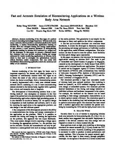
3 RWQ Modeling Examples The RWQ modeling technique outlined above is applied to data generated using the SPICE MOS2 and MOS3 models for an NMOS and a PMOS device using the device dimensions and model parameters shown in Table I. The corresponding RWQ models are referred to as RWQ2 and RWQ3, respectively. For both RWQ2 and RWQ3, su�cient accuracy is obtained with nr = 3 (which means that there are two region boundaries). The quality of the nal
ts are shown are shown in Fig. 2(a){(d). For lack of space, the coe�cients in each region are not shown here, but the
nal values of the con guration parameters are given: (i) RWQ2 NMOS: 1.08, 1.48], (i) RWQ2 PMOS: 0.98, 1.48], (iii) RWQ3 NMOS: 0.38, 0.90], and (iv) RWQ3 PMOS:
0.43, 0.66]. Note that the rst value in each of the above con guration vectors is the slope of the boundaries and the second value is the intercept of the second boundary on the Vds {axis. Further note that the RWQ models implicitly contain the channel-length modulation e ect that is seen in the data (LAMBDA for MOS2 and KAPPA for MOS3 are nonzero in Table I). In the next example, the RWQ modeling procedure is applied to NMOS and PMOS test data obtained from a 256 Mbit DRAM chip. The parameters for the test device are W =10 m, L=0.5 m,
10
4.5 SPICE MOS2 data RWQ2 fit
SPICE MOS2 data RWQ2 fit
10
SPICE MOS3 Data RWQ3 Fit
4
8
3.5 8 3
6 2.5
6
2 Ids
Ids
Ids
4 4
1.5 1
2
2 0.5
0
0 0
1
2
3
4 Vds
5
0 0
1
2
(a)
3
4 Vds
5
0
1
2
3
4
5
Vds
(b)
(c)
1
1.4
SPICE MOS3 Data RWQ3 Fit
256Mb DRAM Data RWQ Fit
256Mb DRAM Data RWQ Fit
5
1.2 0.8 1
4 0.6
0.8
3 0.6 Ids
Ids
Ids
0.4 2
0.4 0.2
1
0.2
0
0 0
1
2
3
4
5
0 0
0.5
1
1.5
2
2.5
Vds
3
3.5
4
0
0.5
1
1.5
2
2.5
Vds
3
3.5
4
Vds
(d) (e) (f) Fig. 2: (a) NMOS level 2, (b) PMOS level 2, (c) NMOS level 3, (d) PMOS level 3, (e) NMOS 256 Mbit DRAM, (f) PMOS 256 Mbit DRAM Table I: SPICE model parameters and device dimensions Parameter Name L (�m) W (�m) TOX (A0 ) UO (cm2 /V.s) VTO (V) NSUB (1/cm3 ) LAMBDA (1/V) VMAX (m/s) KAPPA
Level 2 NMOS PMOS 0.8 0.8 10.0 20.0 250 250 600 300 0.8 -0.9 9.63e14 1.05e16 0.015 0.026 { { { {
Level 3 NMOS PMOS 0.8 0.8 10.0 20.0 203 203 762 254 0.73 -0.97 1.75e16 2.15e16 { { 1.49e5 1.82e5 9.51e-2 3.22e-2
tox=80A0 , and Nsub =1017 /cm3 . In this example, two regions are su�cient to t both data sets� the nal ts are shown in Fig. 2(e) and (f). The values of the con guration parameter (slope) for the NMOS and PMOS RWQ models are 0.69 and 0.76, respectively.
4 Fast Timing Simulation with RWQ models The regionwise quadratic MOS I-V models have been incorporated into a fast timing simulator called ILLIADS2. In ILLIADS2, each simulated node is mapped into the generic MOS circuit primitive 3] shown in Fig. 3. Piecewise-linear input signals are applied at the terminals Di and Gi , the parasitic resistive and capacitive elements are assumed to be linear, and the output node capacitance is denoted by CL . If each MOS transistor in the primitive
has a RWQ model, it can be easily shown that the differential equation for the output node voltage is a Riccati di erential equation of the form dV = KV2 + (p � + p )V + (q � 2 + q � + q )� V(0) = V : 1 0 2 1 0 0 d� (5) This di erential equation permits analytical solutions which are computationally e�cient and numerically stable 3]. To simulate charge-sharing between two nodes, a primitive similar to the one above may be used. The resultant di erential equation is of the same form as (5) if RWQ MOS models are used. During the course of simD1 G1
Dk
Dn gi
Gk
Ci
V(t) CL
Fig. 3: Circuit Primitive ulation, a transistor may change its region of operation. Since the coe�cients of the node di erential equation depend on the region of operation of each MOS transistor in the primitive, determining the time of region crossings is important. This involves solving a nonlinear algebraic
equation. This overhead is kept to a minimum in RWQ modeling by using the smallest number of regions that can accurately t the given data. The procedure in 4] can also be viewed as a special case of RWQ modeling, but since it uses a large number of regions, many region crossings will occur even if the timestep or the voltage change is small, thereby making that method ine�cient. In order to reduce the number of simulated nodes, internal nodes with small loading capacitances are removed by merging serial and parallel transistors. This merging is accomplished by combining the device transconductances to obtain an equivalent transconductance and by combining the gate signals to obtain an equivalent gate signal. In this procedures, there is a tacit assumption that the RWQ models of the merged transistors are the same� the same assumption is also made for conventional MOS models. When capacitances of internal nodes are not negligible, or if the waveforms at these nodes are desired, internal nodes are also simulated along with the driven and pass nodes of the circuit. The simulation of internal nodes and complicated charge-sharing e ects are not discussed here. In brief, we employ a waveform relaxation algorithm in which the primitive of each simulated node is solved in turn by linearizing the waveforms at the other nodes. Body-e ect in MOS transistors was not considered during RWQ modeling, but it is accounted for during simulation by updating the value of the threshold voltage using the latest values of the source-bulk voltage Vsb . For example, body e ect in the upper NMOS transistor of a NAND2 gate can be simulated accurately since the internal node simulation capability provides us with accurate values of the internal node voltage. The accuracy of bodye ect simulation is demonstrated through an example in the next section.
5 Simulation Results with RWQ Models In this section, we demonstrate the accuracy and speed advantage of fast timing simulation with RWQ models by comparing SPICE3 simulations with MOS2 (MOS3) models against ILLIADS2 simulations with RWQ2 (RWQ3) models of Section 3. Simulation results of a CMOS inverter circuit for various input rise-time and output capacitance values are shown in Fig. 4(a) and (b). Next, a CMOS NAND2 gate is simulated using the MOS2 and RWQ2 models and the output and internal node waveforms are shown in Fig. 5(a). The waveforms which result when body-e ect is not considered are also shown. Another example of the accuracy of ILLIADS2 is given in Fig. 5(b) which shows the waveforms at one node in a CMOS four-bit full adder circuit. The above examples demonstrate that by using RWQ models, ILLIADS2 can provide simulation results which are very accurate compared to electrical-level circuit simulation with sophisticated high-level MOS models. In order to demonstrate the e�ciency of ILLIADS2 with respect to SPICE3, the run-times for several benchmark circuits are collected and compared. The results are shown in Table II, where N
refers to the transistor count of the circuit. For the ISCAS85 combinational benchmark circuits (named c*), the input patterns were chosen randomly, whereas for the ISCAS89 sequential benchmark circuits (named s*), we use test vectors obtained from STG 5] as the input sequences. The run-time data shows that ILLIADS2 achieves two to three orders of magnitude speedup over SPICE3 for circuits with up to 2000 transistors. Moreover, the speedup factor is seen to increase with the number of transistors in the circuit. Hence, we expect that the speed advantage will be even more substantial for larger VLSI circuits.
6 Conclusions In this paper, we have described a regionwise quadratic (RWQ) modeling technique that provides the ability to perform fast and accurate timing simulation of MOS digital circuits using highly accurate MOS models. The accuracy of the modeling technique has been demonstrated by applying it to high-level SPICE models and measured I-V characteristic data. The implementation of these models in a fast timing simulator, ILLIADS2, has also been described. ILLIADS2 has been tested on several benchmark circuits and the simulation results have been compared with SPICE3. The results show that (i) the use of RWQ models provides very accurate results, and (ii) fast timing simulation with RWQ models is two to three orders of magnitude faster than SPICE3, and the speedup increases with circuit size. Future work in this area will focus on developing better equivalent capacitance models for submicron MOS devices for use in fast timing simulation.
References
1] D. Overhauser, Fast Timing Simulation of MOS VLSI Circuits. PhD thesis, University of Illinois at UrbanaChampaign, 1989.
2] Y.-H. Shih, Y. Leblebici, and S. M. Kang, \ILLIADS: A fast timing and reliability simulator for digital MOS circuits," IEEE Trans. Computer-Aided Design, vol. 12(9), pp. 1387{1402, Sept. 1993.
3] Y. H. Shih and S. M. Kang, \Analytic transient solution of general MOS circuit primitives," IEEE Trans. Computer-Aided Design, vol. 11(6), pp. 719{731, June 1992.
4] Y. H. Chang and A. T. Yang, \Analytic macromodeling and simulation of strongly coupled mixed analogdigital circuits," Proc. IEEE Int. Conf. on ComputerAided Design, pp. 244{247, Nov. 1992.
5] W. T. Cheng and S. Davidson, \Sequential circuit test generator (STG) benchmark results," Proc. IEEE Int. Symp. on Circuits and Systems, pp. 1938{1941, May 1989.
6
6 SPICE3 ILLIADS2
tr=1ns,C=0.1pf
5 4
tr=1ns,C=10pf
4
tr=1ns,C=10pf
3 Vout
Vout
3
SPICE3 ILLIADS2
tr=1ns,C=0.1pf
5
2 1
2
tr=5ns,C=0.01pf
1
0
tr=5ns,C=0.01pf
0 0
5e-09
1e-08
1.5e-08
2e-08
2.5e-08
0
5e-09
1e-08
1.5e-08
time
2e-08
2.5e-08
time
(a) (b) Fig. 4: CMOS inverter (a) RWQ2/MOS2 models, (b) RWQ3/MOS3 models
6 SPICE3 WITHOUT-BE WITH-BE
5
SPICE3-MOS2 ILLIADS2-RWQ2 SPICE3-MOS3 ILLIADS2-RWQ3
5 4
4
3
Vout
3
2
2
1
1
0
0 0
2e-09
4e-09
6e-09
8e-09 time
1e-08
1.2e-08
1.4e-08
0
1e-08
2e-08
3e-08
4e-08
5e-08
6e-08
7e-08 time
8e-08
9e-08
1e-07
(a) (b) Fig. 5: (a) Output and internal node waveforms of CMOS NAND2, (b) One node of a 4-bit CMOS full adder
Ckt. Name c17 adder4 alu4 c432 c499 s27 s208.1 s641
Table II: Speedup Measurements for ILLIADS2 N
24 144 470 1004 2356 114 624 1740
SPICE3 7.6 356.5 802.9 4030.9 10386.4 70.4 330.5 3376.4
Level 2 ILLIADS2 0.4 4.2 8.1 39.0 58.5 4.2 12.7 36.7
Speedup 19 84.88 99.1 103.4 177.5 16.8 26.0 92
SPICE3 6.2 276.2 987.2 4115.4 14747.2 298.1 686.8 23477.7?
Level 3 ILLIADS2 0.4 3.0 8.2 38.4 45.7 3.7 10.6 35.0
?: Large run-time due in part to DC convergence problems
SPEEDUP 15.5 92.1 120.4 107.2 322.7 80.6 64.8 670.8