38
J. KOLOUCH, FPGA BASED TEST MODULE FOR ERROR BIT EVALUATION IN SERIAL LINKS
FPGA Based Test Module for Error Bit Evaluation in Serial Links Jaromír KOLOUCH Dept. of Radio Electronics, Brno University of Technology, Purkyňova 118, 612 00 Brno, Czech Republic
[email protected] Abstract. A test module for serial links is described. In the link transmitter, one module generates pseudorandom pulse signal that is transmitted by the link. Second module located in the link receiver generates the same signal and compares it to the received signal. Errors caused by the signal transmission can be then detected and results sent to a master computer for further processing like statistical evaluation. The module can be used for long-term error monitoring without need for human operator presence.
Keywords Serial link, bit error rate, LFSR counter, free-space optical link, FPGA.
1. Introduction Serial link arrangements are nowadays often used instead of former parallel forms of data transmission due to their advantages. Among these advantages, especially lower requirements for special electrical, mechanical and other components are valuable. These components are necessary in several items for parallel arrangement whereas, in serial arrangement, only one-bit transmitter and receiver are sufficient. Operations with parallel-to-serial and reverse conversion and with clock reconstruction can be done in standard digital circuitry that is presently available in upto-date digital devices with features as high reliability, low price and possibility for large integration. Serial principle of link arrangement implies higher bit rate in the transmission channel compared to parallel arrangement if the data transfer speed should be equal. The most universal digital devices – monolithic microcontrollers – are limited in this respect (at least with exception for some special devices that are not produced in high volume), if they have to perform necessary conversion and/or other operations. Therefore, programmable logic, especially FPGA devices, represents ideal means for handling the fast link signals. The modern FPGA devices include features that can be of cardinal importance to successful serial link design. Of course, ASIC devices are suitable if sufficient volume of production is reached. A very important feature of a serial link is its bit error rate (BER). Requirements for allowed bit error rate are
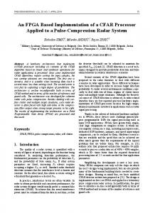
given by standards for serial links. When a link arrangement is designed, it is desirable to check its BER against these requirements. Use of different error-correcting schemes and protocols can mask the individual bit errors so that they are not visible for the user, if BER is not too high. Therefore, these errors should be measured at the lowest level where they can be caught, i.e. at the level of transmitted pulse signal. For this measurement, a FPGA based test module has been built. Two identical modules can be inserted into the link. Then, duplex link operation can be tested. For simplicity, we'll suppose testing of transmission in only one direction in the further description. The transmitter module uses a pseudo-random pulse test signal generated by a LFSR counter included in the test module (LFSR-tx in Fig. 1) that simulates the commonly transmitted user signals. The receiver test module generates internally the same signal called reference signal by identical LFSR counter (LFSR-rx in Fig. 1) and compares it against the received signal. If both signals are found to represent the same binary sequence, then the link transmits the test signal without errors. The transmitter and receiver with test modules will be referred to as the test system. Principle diagram of its arrangement is in Fig. 1. The test signal is generated according to the ITU-T recommendation [2]. The LFSR counter ensures occurrence of pulses and spaces with different length. For n-bit counter implemented in a FPGA device, these lengths vary between 1 and n – 1 bit intervals (clock periods) for pulses, and between 1 and n intervals for spaces, see e.g. [1]. There are other LFSR counter modifications possible, but the common FPGA features like power-on reset imply that counter modification with initial all-zeros counter state is used which gives the mentioned lengths. The FPGA device of Spartan-3 series (Xilinx) contains all that is necessary for both test signal generation in the transmitter and its processing in the receiver. This device has been used in the module described.
2. Data Extraction In the receiver, it is necessary to transform the received signal into data, a stream of zeros and ones, only with the knowledge of the signal bit rate that is given by
RADIOENGINEERING, VOL. 15, NO. 1, APRIL 2006
oscillators in both modules. These oscillators in ideal case should have exactly the same frequency. Nevertheless, in practice, their frequencies are always slightly different, and this difference varies in time. There are two approaches how to perform this transformation:
39
subsequent data evaluation at slightly lower as well as slightly higher rate given by the receiver oscillator frequency than the bit rate of the received signal.
• Use of phase-locked loop (analog approach),
3. Bit Error Detection
• Sampling the input signal at sufficiently high frequency with subsequent digital processing.
For a decision whether the data stream decoded from the received signal represents correct data, the reference signal generated by LFSR counter located in the receiver, that is identical to the test signal generator, is used. The reference signal generator is clocked by the oscillator used for data extraction. To make the comparison of decoded data and the reference signal possible, FIFO memory is used for the transformation of the decoded data into one-bit data stream. To ensure that no overflow of contents in this FIFO memory occurs, the oscillator used for data extraction and for error bit evaluation must have slightly higher frequency than the oscillator in the test signal generator. Therefore, bit intervals where the FIFO does not contain valid data, periodically appear. The comparison is then made only in the bit intervals where the FIFO outputs valid data, and the reference signal generator is clocked only in these bit intervals.
Both these methods rely on occurrence of edges in a received signal. These edges must be sufficiently dense to allow proper extraction of a digital signal. The maximum time interval between two edges in the test signal generated by the LFSR counter is determined by the bit width of the counter, as is mentioned above. The phase-locked loop can yield the recovered clock signal together with data, digital approach extracts only the resulting zero/one data stream. In the designed module, both these approaches were implemented as a possibility to choose. For the phase-lock approach, the Micrel’s SY87700 device with integrated phase-locked loop and other circuitry for clock and data recovery (CDR) was used. Digital data extraction was implemented directly in the FPGA. The digital data extraction from the received signal used in the module, which was suggested by [3], is based on sampling the received signal at the frequency that is approximately 4 times higher than the bit rate of the received signal. In the Spartan-3 device, this can be easily done using the Digital Clock Manager (DCM) block. The oscillator signal represents the input to the DCM, which creates four signals with the same frequency as the input signal, and with the phase shift 0, 1/4, 1/2, and 3/4 of its period. These signals are used to sample the received signal. The signals produced by sampling are then processed by a detection block where changes in the received signal are found by the EXCLUSIVE-OR operation of each two samples that are mutually phase shifted by one quarter of the period. Output signals from this block are then decoded to give the desired data stream. The recovered data stream is synchronized by the block Sync (Fig. 1) to the clock generated by the oscillator located in the receiver (rx-clk in Fig. 1). Due to difference in frequencies of both oscillators, in the test signal generator and in the received signal processing block, an invalid bit or a pair of valid data bits in one bit interval are sometimes present in the decoded signal. This happens periodically if both these frequencies are ideally stable. If the frequency of test signal generator is lower than that of the reconstruction block, then the first possibility comes into being, otherwise two valid data bits periodically occur. Nevertheless, if frequency variations and jitter in both oscillator signals are present, both these situations must be considered as possible. This fact imposes requirement for the output data format of decoder. Along with the two-bit data, two-bit control signal is generated that indicates data bits validity. This setup allows correct data transfer to
LFSR-tx
+
tx-clk test signal
Link
Sync FIFO rx-clk Inequality Comparator
reference signal 1
2
LFSR-rx
error
+
rx-clk Fig. 1. Principle diagram of test system arrangement
It is necessary to synchronize the reference signal generator with the received data stream. The contents of the LFSR counter varies in course of its cycle whose duration is 2n – 1 bit intervals (clock periods) for n-bit counter. The generated signal bit values are unambiguously defined by electrical connection of the counter and by its initial contents. If the decoded data stream is initially connected to the input of the shift register that constitutes the LFSR counter instead of its feedback signal (switch in position 1 in Fig. 1), then, after n bit intervals, the register contents are defined by the data stream. The shift register input can then be switched to the feedback signal (switch in position 2). After that, the LFSR counter in receiver runs in standalone operation mode and generates reference signal that, if no errors in the link appear, is identical to the test signal.
40
J. KOLOUCH, FPGA BASED TEST MODULE FOR ERROR BIT EVALUATION IN SERIAL LINKS
If the test is carried out at a not too high frequency, where the circuitry including FPGA is able to work reliably, and if the disturbing phenomena like electromagnetic interference, signal integrity issues or supply imperfections do not affect the memory elements in the circuitry, the test execution could continue for unlimited time without need for external intervention. The system described is able to sense and register individual errors in the link. When it is amended by a unit that can perform a sort of statistical evaluation or contains interface to a master computer, then it can be used for long term monitoring and reliability evaluation of the link.
re detection can then be based on setting some error rate that is considered as limiting for correct operaion. This decision can be done at the FPGA level, or at higher level (processor in the additional unit, master computer). The flexibility and practically unlimited possibility to change the FPGA configuration allows choosing the criteria for failure detection flexibly according to different test conditions. Decision at the FPGA level should be used if fast response to the detection is required. Decision done at higher level can be suitable if the time necessary for the response is not an important factor.
4. Test Module Setup 3.1 Test System Failure Detection If the test system is used for long term link monitoring that has to proceed automatically without intervention of an operator, it is necessary to assure that there cannot occur a situation where the test modules fail in their operation regardless the receiver input signal and other conditions including those when the requirements for errorless operation are not perfectly fulfilled. It was mentioned above that the data extraction from the input signal rely on sufficient density and regularity of edges in the received signal. If there are errors in this signal, it is possible that this requirement is not met. Then, the synchronization of the reference signal with the received data stream can be lost. Similar situation occurs if, in course of evaluation, contents of the test or reference signal generator is corrupted, or if an error in the data extraction like false bit insertion or loss of a valid bit in the FIFO occurs. On that situation, the subsequent comparison gives results with errors that appear as randomly distributed in the data stream – it can be approximately said that half of the received bits are evaluated as correct, other half as errors. Such error reports indicate incorrect test module operation. The corresponding state of the test system then represents its failure. The system then cannot recover into errorless operation if this possibility is not taken into account in the module design. Therefore, a mechanism that detects the system failure and invokes re-initialization of the system must be included.
Fig. 2. PCB board with test module.
Usually, the bit error rate in real links is low, far lower than the error rate indicated in case of system failure. The failu-
The module is built on a 4-layer PCB board (Fig. 2). The switching supply arrangement (its coil can be seen in the figure) ensures high efficiency and low power losses even in high range of input supply voltage, what is important in the dense packing that is commonly used in link installations. The four layers allow preserving constant characteristic parameters of the high-speed signal traces what is required to ensure signal integrity. High-speed input and output signals are buffered by PECL devices that can be directly interfaced to the FPGA as well as to the CDR device. A FPGA device of type XC3S200-5PQ208C is used for the error detection and basic data processing. A Rabbit microcontroller block RCM2200 with internet interface is attached to the board. The FPGA accumulates the basic test results in 1 millisecond time intervals, and every second it issues an interrupt signal to the controller that reads the results and, after some processing, sends them via internet to a master PC. This setup allows carrying out the test without interruption caused possibly by the communication with the master. All features like level of decision for re-initialization, initial data processing and similar can be flexibly adapted to needs of a particular application by programming the microcontroller and FPGA.
5. Use of the Module for Free Space Optical Link Monitoring The test module has been designed primarily for testing the free-space optical (FSO) link, although it can be in principle used for testing any serial link. There are some features specific to FSO link that affect the obtained result. In many other link types, errors appear mainly in form of individual corrupted bits caused by interfering processes of pulse character. This type of errors can be well caught and evaluated by the module. In FSO link, there are other processes that can cause errors in data transfer. If an obstruction like a flying bird can move into the optical beam, the data sensed by the link receiver disappear for the time of obstruction presence. According to the receiver setup, a constant logic level or noise-like signal is provided on its output. This situation usually means that edges in the signal that are necessary for correct data extraction disappear or there are quite false and ran-
RADIOENGINEERING, VOL. 15, NO. 1, APRIL 2006
41
domly distributed edges. Both possibilities can cause system failure described above.
tion from the received signal, bit error detection and possibility of system failure handling are discussed.
Another problem has been found at transmission rates above 100 Mb/s. Even clear atmosphere introduces jitter into the signal that can cause appearance of errors or system failure in some conditions, whereas in other time period, apparently in the same conditions, the transmission is without errors. Other error types can be caused by atmospheric influences like fog or rain. Impact of these influences will be investigated in future work.
The module can be used for long-term error monitoring without need for human operator presence, especially in free-space optical links and similar arrangements.
6. Conclusion In the paper, a FPGA-based test module for serial links is described. To perform the test of bit error rate, one module that generates pseudorandom pulse signal is inserted into the link transmitter. This signal is transmitted by the link and compared to the same signal generated in the link receiver by the second module. Differences between these two signals represent errors caused by the transmission (and possibly by the transmitter and receiver arrangement). The module can perform some preliminary processing of the results. Then, these results can be sent to a master computer for further processing like statistical evaluation. Some problems concerning to the data extrac-
Acknowledgements The work described in the paper has been supported by the Grant Agency of the Czech Republic under the contracts No. 102/05/0732, by the Czech Ministry of Education under grant No. 130/2005 and by the research program MSM 021630513.
References [1] ABRAMOVICI, M., BREUER, M. A., FRIEDMAN, A. D. Digital Systems Testing and Testable Design. J. Wiley and Sons, Inc., 1995. [2] Recommendation of ITU-T O.151, 1992. [3] SAWYER, N. Data Recovery. XAPP224, Xilinx, 2005. [4] WILFERT, O., KOLKA, Z., BIOLKOVÁ, V. Free-space optical communication. In Proc. of Optical Communications 2004. Prague, 2004, p. 207 – 216. [5] KOLOUCH, J., KOLKA, Z. Embedded data tester for FSO links. In Proc. of EDS 2005. Electronic Devices and Systems International Conference, Brno, 2005, p. 39 – 43.
Book Review WAKERLY, John F.: Digital Design: Principles and Practices 4th Edition, Pearson Education Inc., 2005 Four editions of this textbook that appeared in time intervals of about five years (first in 1990) provide evidence of this book´s quality and readers´ interest. It covers topics addressing a beginner as well as many of those which a professional digital designer needs in his work. Basic concepts of number systems and codes, TTL and CMOS families of logic devices and of their use in combinational and sequential digital subsystems are explained. Then, some modern topics as metastability and synchronizers, memories and programmable logic are introduced. Microprocessors are not discussed – I consider this rather an advantage because they would extend the book too much and a lot of specialized publications in this field are available. Many sample designs with interesting comments demonstrate how traditional 74-series digital devices can be used. In the latest edition of this textbook, these designs are then re-written in the three of today´s most often used hardware design languages – ABEL, VHDL and Verilog, allowing their implementation into PLD and FPGA devices, again with practical experience added. Comment boxes are attached with many valuable advices and explanations. The book is written in fresh and readable style, with an extraordinary sense of the needs of the reader who is not an expert in the field. As to my own experience, I tried several books to learn Verilog as a complementary tool to ABEL and VHDL; both of them I have been using for
years. Wakerly´s text is the first that I managed to read in one or two days with a feeling that I understand this language so well that now I am able to write descriptions in it. Along with the book itself, web-based accompanying information is provided containing further topics that would add too much pages in the printed version, nevertheless, some readers may be interested in it. Of course, some objections can be made, no such book would completely avoid them. For example, some more complicated digital designs like 16-bit ALU with group-carry lookahead would today hardly be designed using the 74 series, and their detailed design including schematic printed in the book does not seem to be very useful. Or, a more up-to-date type of FPGA could be chosen as representative for explanation. But similar objections can only be raised to a really minor part of the book. I can recommend this book to a wide audience, from students who will start with digital design to experienced designers that have so far been using traditional design methods and would like to become acquainted with modern approaches using HDLs and programmable logic, or simply would like to have a good reading. Of course, to become an expert in the field, a further study is necessary, but the book gives a base on which it is possible to build. Jaromír Kolouch