FREE-p: Protecting Non-Volatile Memory against both Hard and Soft Errors Doe Hyun Yoon†
[email protected]
Naveen Muralimanohar‡
[email protected]
Jichuan Chang‡
[email protected]
Parthasarathy Ranganathan‡
[email protected]
Norman P. Jouppi‡
[email protected]
Mattan Erez†
[email protected]
†
The University of Texas at Austin Electrical and Computer Engineering Dept. Abstract Emerging non-volatile memories such as phasechange RAM (PCRAM) offer significant advantages but suffer from write endurance problems. However, prior solutions are oblivious to soft errors (recently raised as a potential issue even for PCRAM) and are incompatible with high-level fault tolerance techniques such as chipkill. To additionally address such failures requires unnecessarily high costs for techniques that focus singularly on wear-out tolerance. In this paper, we propose fine-grained remapping with ECC and embedded pointers (FREE-p). FREE-p remaps fine-grained worn-out NVRAM blocks without requiring large dedicated storage. We discuss how FREE-p protects against both hard and soft errors and can be extended to chipkill. Further, FREE-p can be implemented purely in the memory controller, avoiding custom NVRAM devices. In addition to these benefits, FREE-p increases NVRAM lifetime by up to 26% over the state-of-the-art even with severe process variation while performance degradation is less than 2% for the initial 7 years.
1. Introduction Non-volatile memory (NVRAM) technologies are emerging as a scalable substitute of DRAM as main memory. For example, phase-change memory (PCRAM) is almost as fast as DRAM (only 2-3× higher latency at the same bandwidth), provides larger capacity, and scales better. However, most NVRAM technologies, including PCRAM, have finite write endurance; memory cells wear out after a certain number of writes. Recent architectural research has focused on this write endurance issue but this prior work is incomplete for three important reasons: (1) it
‡
Hewlett-Packard Labs Intelligent Infrastructure Lab. relies on integrating custom error-tolerance functionality within memory devices – an idea that the memory industry is historically loath to accept because of strong demand to optimize cost per bit; (2) it ignores soft errors (in both peripheral circuits and cells), which can cause errors in NVRAM as shown in recent studies; and (3) it requires extra storage to support chipkill that enables a memory DIMM to function even when a device fails. We propose Fine-grained Remapping with ECC and Embedded-Pointers (FREE-p) to address all three problems. Fine-grained remapping nearly eliminates storage overhead for avoiding wear-out errors. Our unique error checking and correcting (ECC) component can tolerate wear-out errors, soft errors, and device failures. The proposed mechanism shifts resiliency functions entirely to the memory controller, leaving NVRAM devices as simple and cheap as possible. Prior research focused on protecting NVRAM only against wear-out failures, ignoring soft errors and device failures. The motivation has been that NVRAM cells are inherently robust against particle strikes. Unfortunately, recent work [5] identified new soft-error mechanisms that impact NVRAM, which we summarize in Section 2.1. Further, memory cells typically account for only 60% of the die area with the rest used for global and peripheral circuits, which are still susceptible to soft errors [32]. Recent architecture research on error-tolerance in NVRAM systems ignores this important source of errors. Simply augmenting existing mechanisms, such as dynamically replicating memory (DRM) [10] and error correcting pointers (ECP) [22], with the techniques for soft-error tolerance used in current DRAM-based systems requires too high an overhead. Moreover, existing NVRAM reliability solutions often require custom functionality embedded within NVRAM devices. ECP, for example, implements hard error detection/correction logic within an NVRAM device. Embedding reliability mechanisms
at the device increases the cost of memory and the protection level is fixed at design-time. It also protects only cell array; hence, it does not achieve end-to-end protection. As practiced in DRAM and FLASH, it is better to implement error detecting/correcting at the memory controller so that we can even detect and correct errors in wires, packaging, and periphery circuits in addition to errors in memory cells. FREE-p is the first mechanism that is designed specifically to tolerate both soft and hard errors in NVRAM main memory systems without error tolerance functionality within the NVRAM devices themselves. FREE-p relies on a novel fine-grained remapping (FR) mechanism that has almost zero storage overhead initially and dynamically adapts to wear-out failures. The innovation is in utilizing the still-functional cells of worn-out memory blocks to store remapping information. We then integrate FR with specially designed ECC for detecting and correcting both hard and soft errors. Unlike prior work, our mechanism can be easily augmented to support chipkill-correct. FR, however, incurs a performance overhead. When accessing a remapped block, the memory controller first reads the original location, and then follows the pointer to the remapped location. This increases memory traffic and access latency, potentially degrading performance. To mitigate the negative impact of FR, we propose a set of optimization techniques to accelerate remapping, including simple caching and a more effective hashbased scheme. We implement all the necessary functionality except the additional storage for ECC (limited to under 12.5% typical in current systems) at the memory controller, enabling end-to-end protection with simple (and expected commodity) NVRAM devices. Compared to the most efficient prior work, ECP, FREE-p achieves 7.5% and 26% longer lifetime at typical and high process variation. These advantages are in addition to tolerating soft errors and potential chip failures. The performance impact of the fine-grained remapping is negligible in the first 7 years of operation, less than 1.8% on average, and is around 10% on average even near end of life (8.8 years). The rest of the paper is organized as follows: We briefly review failure mechanisms in PCRAM and related work in Section 2; we present FREE-p in Section 3; we evaluate the wear-out tolerance and performance overhead of FREE-p in Section 4; and Section 5 concludes the paper.
2. Background and related work Our technique, FREE-p, is applicable to any nonvolatile memory technology but we use PCRAM as an
example technology in this paper. We first describe basics of PCRAM as well as failure mechanisms in Section 2.1, and discuss related work in Section 2.2.
2.1. Failures in phase-change memory PCRAM operations. PCRAM is a non-volatile memory built out of Chalcogenide-based materials such as alloys of germanium, antimony, or tellurium (Ge2Sb2Te5, GeSb, Sb2Te3). Unlike DRAM and FLASH that record data through charge storage, PCRAM uses distinct phase-change material states (hence, resistances) to store values. Specifically, when a phase-change material is heated to a high temperature for an extended period of time, it crystallizes and reduces its resistance (SET operation). The SET operation is slow, and determines the write latency of PCRAM. To RESET a cell into a high resistance state, a current large enough to melt the phase-change material (almost double the SET current) is applied for a short period, and then abruptly cut-off. The abrupt current fall quenches the material into the amorphous phase, resulting in high resistance. A promising feature of PCRAM is its capability to store multiple bits in a single cell, also referred to as Multi Level Cells (MLC). The pulse width of RESET for MLC is adjusted such that it partially crystallizes the phase-change material and modifies its resistance to an intermediate value between SET and RESET resistances. ITRS projects the availability of 4-bit MLC by 2012 [1]. Reading a cell simply involves sending a small current and measuring the voltage drop across the cell. As both crystalline and amorphous phases are relatively stable at normal operating temperature (more about this later), the cell can ideally retain the value for many years. Hard Errors in PCRAM. While high operating temperatures, required for SET/RESET operations, help keep PCRAM cells stable at room temperature, they significantly impact the lifetime of PCRAM. After repeated high temperature RESET operations, the electrical path through the phase-change material begins to break and this permanently RESETs the cell into a high resistance state. Recent studies on PCRAM prototypes show that the number of writes to a PCRAM cell is limited to 108-1010 [5] while a DRAM or SRAM cell can support more than 1015 writes. This significant difference in endurance between PCRAM and volatile memories is considered a critical drawback that precludes PCRAM from becoming a universal memory. Going from cell to chip, PCRAM chip endurance (based on vendor specifications such as [16]) can further drop to 106 due to process variation and nonideal wear-leveling.
Soft Errors in PCRAM. Although PCRAM is robust against particle-induced soft errors, there are several factors that can cause soft errors in PCRAM. Some common factors include write noise, resistance drift (or short-term drift), and spontaneous crystallization (or long-term drift). In particular, the short-term resistance drift is prone to causing soft errors in PCRAM but has received little attention from the architecture community. Write noise (also called thermal crosstalk) refers to disturbances in a cell value due to repeated SET/RESET operations on a nearby cell. Studies on PCRAM reliability, however, show crosstalk is not an issue [17, 12]. The root cause of short- and long-term resistance drifts lies in the metastable nature of the amorphous phase. After the sudden cooling of a PCRAM cell that triggers the state change, the resistance of the cell continues to grow for a certain period of time before it starts reducing again. This phenomenon is referred to as short-term drift. Longterm drift is a result of slow crystallization of the phasechange material at room temperature, which degrades the cell resistance over time. As the rate of crystallization is directly proportional to temperature, it can take many days to produce a noticeable change in cell resistance at room temperature. Long-term drift can be easily addressed by periodically refreshing cells every several days. However, short-term drift can be problematic in PCRAM, especially for multi-level cell (MLC) PCRAM. The random nature of short-term drift due to process variation makes it difficult to guarantee correctness through periodic refreshing or scrubbing. In addition to soft errors in the PCRAM cells themselves, the peripheral circuits such as decoders, sense-amps, and repeaters still use CMOS transistors that are susceptible to soft errors. With memories typically having area efficiency (ratio of area of memory cells to the total area) of less than 60% [32], the likelihood of a failure in peripheral circuits is nontrivial. Chip Failures. In addition to soft and hard errors in memory arrays, a recent study shows memory chip failures, possibly due to packaging and global circuit issues, cause significant down time in datacenters [23]. Hence, business critical servers and datacenters demand chipkill-correct level reliability, where a DIMM is required to function even when an entire chip in it fails. There are various solutions for chipkill-correct [6, 3, 33, 27] and the industry is pursuing even stronger protection [8, 15], for example, double chipkill or soft error correction under chipkill. With memory manufacturers’ relentless focus on cost per bit, PCRAM memories will likely require very robust fault tolerance techniques as well. For these reasons, in addition to
wear-out protection, traditional coding techniques such as ECC and parity will be required to tolerate PCRAM chip failures.
2.2. Related work Many techniques have been recently proposed to improve NVRAM endurance, focusing on write reduction and wear-leveling to increase lifetime (Section 2.2.1) and hard error detection/correction for graceful degradation (Section 2.2.2). We also discuss other prior work (Section 2.2.3). 2.2.1. Increasing NVRAM lifetime. Avoiding unnecessary writes. Researchers have developed various techniques to avoid unnecessary writes. Lee et al. [13] proposed to only write back modified cache lines or words. Qureshi et al. [19] also explored writing back only modified data. A variety of fine-grained approaches (bit-level partial write) have also been proposed, including data comparison write (DCW) [31], Flip-N-Write [7], and many others [36, 34, 11], by utilizing read-before-write to detect modified data and potentially selectively invert bits. Wear-leveling. Another approach to improve lifetime is by distributing writes equally to all cells in the device. This technique is known as wear-leveling and is commonly used with FLASH memory. Prior research on PCRAM wear-leveling includes row shift [36, 22], word shift [34], and randomized address mapping [19, 18, 24]. Our work focuses on soft and hard error tolerance with commodity NVRAM devices, and can be combined with any lifetime-improvement techniques. 2.2.2. Tolerating wear-out failures. We first present prior wear-out failure detection/correction schemes, and then explain the extra actions needed once such mechanisms become insufficient due to a large number of failures. We also describe one of the most advanced prior proposals, ECP, in detail. Detecting/correcting wear-out failures. The most intuitive approach to detect wear-out failures is to use an ECC code. The complexity of ECC-based error correction, however, increases linearly with the correction capability [26], rendering general ECC unsuitable for NVRAM [10, 22]. An entirely different approach to detecting wear-out errors is to use verify-after-write, in which detection happens when writing to NVRAM. Verify-after-write first writes a data block to NVRAM and then immediately reads the value for comparison. A mismatch indicates a write failure due to wear-out. Verify-after-write incurs high traffic and performance
overheads if implemented at the memory controller and recent work advocates implementing this functionality within the NVRAM devices themselves [10, 22]. Because an NVRAM write is relatively slow, it is generally believed that the penalty of adding an internal read after the write is not significant. A caveat is that the verifying reads increase power consumption even when there is no wear-out failure. After error detection, errors are corrected by using another, non-faulty set of cells to store the data. Two recent techniques have been suggested to accomplish this. Dynamically replicating memory (DRM) [10] replicates the write to a separate NVRAM page with disjoint failures, and future reads access both pages to retrieve the correct data. Later research [22], however, shows that even a simple ECC scheme with a single-bit error correcting and double-bit error detecting (SECDED) code outperforms DRM. A promising alternative, ECP [22], can tolerate wear-out failures without multiple accesses, but further modifies NVRAM devices. ECP implements all error-correcting functionality within the NVRAM device: it uses verify-after-write to detect errors, a set of pointers to encode error locations, and additional storage cells to hold patched values. For a 512-bit data block, a 10-bit error correcting entry can tolerate one bit failure (9 bits to identify the error location and 1 bit to hold the patched value). The 6-bit tolerating ECP (ECP6) uses 6 such 10-bit entries, and has a 12% static overhead. Although correcting multibit errors with ECP is much simpler than with traditional error codes (e.g., BCH codes), ECP has several significant limitations. − ECP can tolerate only wear-out failures. Augmenting ECP to achieve end-to-end reliability will result in high storage overhead. − The hard error tolerance level with ECP is fixed and determined at device design time. Due to process variation and non-ideal wear-leveling efficiency 1 , the overhead of ECP is unnecessarily large. − ECP requires custom NVRAM devices. DRAM and FLASH manufactures are highly motivated to minimize cost per bit, and would prefer solutions without custom logic in the NVRAM devices for simplicity, flexibility, and cost advantages. Recent work, SAFER [25], proposes a better mechanism compared to ECP to tolerate hard failures in PCRAM. While it is orthogonal to our work, similar to ECP, SAFER also requires a custom-designed PCRAM device. 1
We use “normalized endurance” proposed by Qureshi et al. [18] as the metric for the efficiency of wear-leveling, which is 90%, at most, using one of the best practical wear-leveling mechanisms.
FREE-p departs from this recent work on tolerating NVRAM errors. We focus on end-to-end reliability rather than on wear-out errors, and also restrict ourselves to current best-practice constraints: (1) we keep storage devices optimized for cost per bit, and implement all resiliency functionality at the memory controller; and (2) we tolerate wear-out, soft errors, and potential device failures with less than 12.5% storage overhead. 2.2.3. Other related work. There has been other prior work that uses pointers and fine-grained data remapping. Wilkerson et al. presented a bit-fix technique [29] that stores pointers as meta-data similar to ECP [22]. Our technique differs in that a pointer is stored within a data block itself and used for finegrained data remapping rather than error correction. Roberts et al. coupled two cache lines assuming one will function if the other fails [21] similar to the DRM approach [10]. Wu et al. presented fine-grained data relocation for migrating frequently accessed cache lines to faster storage. This technique uses cache “tags” for managing fine-grained data relocation. Instead, we use embedded pointers for fine-grained data remapping.
3. FREE-p implementation This section describes our proposal for an end-toend reliable NVRAM memory system with commodity devices and FREE-p. We start by describing finegrained remapping (FR), our low-cost wear-out failure tolerance mechanism, in Section 3.1. In Section 3.2, we explain how to use FR to design an NVRAM-based memory system with all necessary reliability mechanisms implemented at the memory controller, leaving NVRAM devices simple. We identify overheads and propose a set of optimization techniques to mitigate the potential performance degradation in Section 3.3. We then discuss hard/soft error detection and correction in Section 3.4 followed by required operating system support in Section 3.5 and chipkill support in Section 3.6.
3.1. Fine-grained remapping As described earlier, current wear-out failure tolerance techniques are designed to tolerate up to a certain number of errors in a memory block. When a block accumulates more wear-out failures than can be corrected, it gets disabled and remapped. The primary problem with the existing techniques is that the remapping and the disabling of data blocks happen at a coarse granularity of a device or OS page. For example, the FLASH controller disables device pages that can no
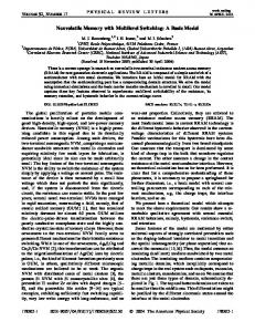
Data page
Block with a failure Ptr
Ptr
Data
Ptr Ptr
Data
D/P flag
Page for remapping
Figure 1. Example of fine-grained remapping with an embedded pointer. longer be used [14]. Most recent work on NVRAM does bit-level error correction prior to remapping [22]. Although coarse-grained techniques are simple to implement (through OS virtual to physical mapping table), they are inefficient. A single 64B block with intolerable failures triggers the mapping out of an entire large page of data of 4kB or more. In contrast to coarse-grained approaches, we propose fine-grained remapping (FR); FR maps out only a small block that contains wear-out failures, leaving the rest of the physical page usable. This both increases the lifetime of a page and makes NVRAM more tolerant to process variation. For instance, prior studies on process variation show strong spatial correlation between memory cells [9] 2 . Hence, it is likely that several consecutive bits in NVRAM can fail well in advance compared to the vast majority of other bits in a page. Without FR, a single cache line failure will deactivate an entire page, leading to poor efficiency. Further, FR adapts to imperfections in wear-leveling more efficiently. Although it is desirable to keep the remap size as small as possible, we use the last level cache line size (e.g., 64B) as the granularity for remapping. While solving the problem of disabling coarse-grained blocks, FR requires a large book-keeping storage. Maintaining all of the remapping information in dedicated storage within the processor or in main memory is impractical. We make a key observation that even if a block is deemed dead, it still has many functional bits that can store useful information. We propose using the remaining working bits in a dead block to embed a remapping pointer, as shown in Figure 1. Thus, we use the mapped-out block itself, otherwise useless, as free storage for remapping information. In addition, we need dedicated storage to indicate whether a block has been remapped; only 1 bit per block. When we detect a wearout failure, we remap the block to a fault-free location, mark that this block is remapped (using a 1-bit Data/Pointer flag (D/P) per data block), and write the embedded remapping pointer within the faulty block. 2
For evaluating our proposals, we conservatively model only random variation.
Figure 2. Chained remapping example (solid pointers) and limiting the number of hops (dashed pointer). The operating system is responsible for identifying a remap region for the failed block (more on this in Section 3.5). In this way, the size of NVRAM degrades gracefully with age. Because the embedded pointer is stored in essentially a faulty memory block, we must ensure that it can be correctly accessed. A pointer is much smaller than the data block it is remapping, and we can therefore use a very simple and strong error code. For example, we can even use a 7-modular-redundancy (7MR) code, which replicates the 64-bit pointer 7 times. If the pointer cannot be correctly stored, even with this large redundancy, we map out the entire page as in current techniques. This, however, should be very rare considering the strength of the 7-MR code (the probability that 7-MR cannot tolerate 4-bit failures is roughly 9.04e-7, assuming uniform errors). We do not consider further wear-out failures on pointers and the D/P flag because we rarely re-write them. A potential problem with FR is chained remapping when a remapped block is remapped again, as shown in Figure 2 (solid arrows). An access to this chained remapping will traverse a linked list, which may take a long time. We eliminate such chains by writing the final destination to the original faulty block when a remapped block is remapped again (dashed arrow in Figure 2).
3.2. NVRAM system organization In this subsection, we show how to use FR and ECC to design a memory system with simple, expected commodity, NVRAM devices. We explicitly explore this as an alternative to the approach of prior research (e.g., ECP [22]) that recommends significant changes to the internal design and micro-architecture of NVRAM components. Figure 3 illustrates a FREE-p memory controller and NVRAM organization. It is much like current DRAM systems: eight ×8 devices construct a 64-bit wide channel and a dedicated device stores the meta-data, which includes the D/P flag as well as ECC information. We assume a DDR3-like interface (burst 8) for NVRAM devices in this study. The main change
Memory controller
Read
Write Req Queue
ABUS
RD Data
DBUS
ABUS
D/P
D
Read Req Queue decode
(a) A read from a normal block x8
x8
x8
x8
x8
x8
x8
x8
x8
Read Data Queue
First Read (pointer)
72-bit wide DBUS
NVRAM
Write Data Queue
ABUS
Reschedule
RD
Second Read
RD Ptr
DBUS D/P
Data
P
D
(b) A read from a remapped block
Figure 3. Memory controller and NVRAM organization. The gray device is for D/P flag and ECC. to the memory controller is support for fine-grained remapping, detailed below for read and write operations. Read operations. When we read data from NVRAM, we also read the D/P flag and identify whether a block is remapped or not. If the block is not remapped, the memory controller forwards the returned data to the upper level, e.g., cache controller, as in a standard memory controller (Figure 4(a)). Otherwise, the memory controller decodes the pointer, re-inserts the request onto the read queue with the remapped address, and schedules the forwarded read request (Figure 4(b)). Thus, reading remapped data requires no interaction with the processor core but incurs bandwidth and latency overheads for the second read. We propose mechanisms to mitigate these overheads in Section 3.3. Write operations. Write operations with FR are trickier than reads. Because we do not rely on any functionality in NVRAM devices, the memory controller must make sure that the target block in NVRAM has not been previously remapped before issuing a write. Otherwise, we may accidentally overwrite the embedded pointer with new data (which will never succeed because of wear-out failures). Hence, we first read the data block from memory before writing data. If the block is not yet remapped, we write the new data to the block (Figure 5(a)). Otherwise, we write the new data to the remapped location using the pointer (Figure 5(b)). Though a write-back is not on the critical processing path, always reading a block before a write is inefficient. With an order of magnitude difference between read and write latency in PCRAM, the overhead of performing a read before a write has minimal impact on performance (