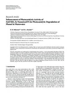
INSTITUTE OF PHYSICS PUBLISHING
NANOTECHNOLOGY
Nanotechnology 17 (2006) 4912–4916
doi:10.1088/0957-4484/17/19/022
Ge dots embedded in SiO2 obtained by oxidation of Si/Ge/Si nanostructures T Stoica1,3 and E Sutter2 1 Institut f¨ur Bio- und Nanosysteme (IBN-1), Forschungszentrum J¨ulich GmbH and CNI—Center of Nanoelectronic Systems for Information Technology, D-52425 J¨ulich, Germany 2 Center for Functional Nanomaterials, Brookhaven National Laboratory, Upton, NY 11973, USA
E-mail:
[email protected]
Received 13 July 2006, in final form 20 August 2006 Published 11 September 2006 Online at stacks.iop.org/Nano/17/4912 Abstract Selective epitaxial growth was used to fabricate narrow Si/Ge/Si pillar nanostructures in small holes in ultrathin oxide (UTO) on Si(100). The self-assembled holes with diameters of 5–30 nm were obtained by in situ partial removal of the UTO at high temperature. The UTO formation and the annealing process were optimized for a high density of holes. The SiGe nanopillars were grown with sizes determined by the initial hole diameter in the UTO. Crystalline Ge dots embedded in oxide were formed by oxidation of the pillar nanostructures. High-resolution transmission electron microscopy (HRTEM) was used to study the pillar nanostructures and the dot shapes before and after oxidation. Capacitors obtained with the oxidized samples showed a hysteresis in their C –V curves attributed to charge retention in the Ge dots embedded in the oxide. (Some figures in this article are in colour only in the electronic version)
1. Introduction Nanodevices based on Si and Ge nanocrystals are of large interest due to the compatibility of the required processes with the well-established silicon technology. In particular, Si and Ge dots embedded in oxide are studied for floating gate memories [1–3] and single electron nanotechnology [4]. The optoelectronic properties of Si and Ge dots [5–7] are of scientific and technological interest due to the novel electronic properties of these zero-dimension systems relative to their bulk and layer counterparts. An advantage of Ge dots embedded in oxide over Si dots is related to the smaller gap of Ge corresponding to lower energies for injected holes or electrons. This results in a higher charge retention time at the same injection voltage. The large difference between the oxidation energy of Ge (−119 kcal mol−1 ) and Si (−204 kcal mol−1 ) (reference [14] in [8]), leads to an increased probability for Ge segregation into clusters in a SiO2 matrix. It is known that during high-temperature oxidation of SiGe alloys, Si is preferentially 3 Author to whom any correspondence should be addressed.
0957-4484/06/194912+05$30.00
oxidized while Ge is rejected from the oxide [8–12]. For high Ge concentration alloys, Ge accumulation at the oxide/SiGe interface, as well as on top of the oxide layer was observed after oxidation of a uniform SiGe layer [8]. The mechanism is not completely understood and different oxidation models are presently being discussed [13–16]. In comparison with the oxidation of SiGe layers, the oxidation of layers with Ge islands is complicated due to non-uniformities in Ge thickness and stress variations [17]. Achieving oxidation all around the islands requires a configuration such that they are not connected by a continuous wetting layer. Otherwise, Ge piles up at the oxide/substrate interface, forming a Ge-rich layer and no oxidation under the Ge dot can be achieved. However, formation of random Ge dots embedded in oxide was demonstrated using ultraviolet assisted low temperature oxidation of SiGe layers [18, 19]. There are also numerous reports on Ge dots embedded in SiO2 obtained from layers deposited and oxidized by different methods, such as: dc magnetron sputtering [20–22], electron-beam evaporation [23, 24], epitaxial Ge islands on subnanometre thick oxide films [25], Ge implantation [26–28], chemical vapour deposition on oxide [29], sol–gel deposition [30],
© 2006 IOP Publishing Ltd Printed in the UK
4912
Ge dots embedded in SiO2 obtained by oxidation of Si/Ge/Si nanostructures
molecular beam Ge deposition on oxidized Si substrates [31]. Charging and memory effects due to the tunnelling of holes or electrons into Ge dots embedded in oxide were demonstrated and studied by different methods as well [2–4, 22–27, 32–35]. Most of the reported results are for a statistical distribution of the dots on the sample surface. However, for future nanodevices the uniformity and precise placement of the dots are very important. Oxidation of ordered islands formed on narrow mesas of isolated islands (single island on a mesa), selectively grown in small windows offers a possible solution [36]. In this case the role of the mesa is twofold, first in inducing the ordering of islands and second in allowing the lateral side oxidation of the pillar mesas, including the oxidation underneath the Ge dots. Focus ion beam or e-beam lithography can be used for precise positioning of holes in the SiO2 /Si substrate followed by epitaxy performed selectively in the holes in ultrathin oxide (UTO) with only 1–2 nm thickness [37, 38]. We expect then that if Si/Ge/Si pillar structures are uniformly grown by selective epitaxy in an intentionally and uniformly preformed array of holes in oxide, a uniform distribution of Ge dots embedded in oxide will be obtained for charge injection-retention devices. In this paper we investigate the formation and the lateral side oxidation of Si/Ge/Si nanopillars selectively grown in holes in UTO using high-resolution transmission electron microscopy (HRTEM). A high density of holes with different diameters within the range 5–30 nm is obtained in which the nanopillars are formed. We use the resulting spreading of the pillar sizes to our advantage to study Ge dot formation by oxidation of Si/Ge/Si nanopillars as a function of pillar size. Capacitors with Ge dots embedded in oxide on pSi substrates show a large hysteresis in C –V curves due to positive charging of Ge dots. The studies are important for obtaining precisely localized crystalline dots in oxide, using selective growth epitaxy.
2. Experimental details The selective epitaxial growth was carried out on pre-patterned Si(100) substrates. The Si substrates were cleaned ex situ using dilute RCA chemistry which results in the formation of a chemical UTO with a thickness of ∼1 nm. The UTO was then self-patterned during in situ annealing at 800 ◦ C at 8 × 10⁻⁸ Torr for 1–2 min immediately before deposition. During these optimized ex- and in situ cleaning procedures we obtained samples with a high density of holes in the UTO on Si substrate. Pillars of a Si/Ge/Si nanostructure were grown in the holes in the UTO on Si by low pressure chemical vapour deposition at 700 ◦ C, with H2 as a carrier gas at a total pressure of 0.2 mbar. The nominal structure under investigation in this paper corresponds to the sequence Si(6 nm)/Ge(1.2 nm)/Si(7.5 nm)/Si substrate for large area deposition. The layer thicknesses were measured by Rutherford backscattering spectroscopy on samples with the UTO completely removed. The structure investigation of the nanopillars before and after oxidation was carried out by cross-sectional transmission electron microscopy (XTEM) in a JEOL JEM 3000F field emission microscope. Samples with pillar structures were further oxidized at 750 ◦ C to form an oxide layer with thickness ranging between 15 and 40 nm. The
(a)
100nm
(b)
100nm
Figure 1. AFM images of: (a) substrate with high density of holes in UTO obtained by annealing in vacuum at 800 ◦ C; (b) Si/Ge/Si nanopillars selectively grown on the prepatterned substrates from (a).
oxide thickness was measured by ellipsometry and corresponds well to a mean value determined from the TEM investigation. Further C –V curves were measured on capacitors obtained from oxidized samples using Al as top electrodes with different areas.
3. Results and discussions 3.1. High-density SiGe pillars First we optimized the ex- and in situ cleaning procedures. We were able to obtain samples with a high density of holes in the UTO on Si substrate. Figure 1(a) shows a typical AFM image of a high density (∼4 × 1010 cm−2 ) of small holes (diameter smaller than 50 nm) in the UTO layer on pSi(001) substrate. The Si/Ge/Si pillar nanostructures formed in these holes in the UTO are shown in the AFM image in figure 1(b). The comparison of the pre-patterned sample before (figure 1(a)) and after (figure 1(b)) the pillar formation shows a direct correspondence between the holes in the UTO and the formed pillar nanostructures. The shape of Si/Ge/Si pillars was found consistently to depend on the diameter of the holes as demonstrated in the high-resolution TEM images in figures 2(a)–(c). For very small holes (below 7 nm in diameter) the pillars grow with a pyramidal shape (figure 2(a)) with (111) contact facets to the Si substrate surface and a very small (001) facet on top. With increasing hole diameter, the nanopillars assume a more complicated shape. The (111) facets become larger and are predominant for bigger SiGe pillars (figures 2(b) and (c)) with aspect ratio varying between 0.8 and 0.9, for width bigger than 10 nm. All the pillars show a vertical (011) contact facet and the (111) facets appear lifted. A similar incorporation of the (011) facet was observed in micron-size Si mesas grown on patterned SiO2 and SiGe islands obtained by dewetting of ultrathin Si-on-insulator [39]. It seems to be driven by the slight overgrowth of the oxide surface which leads to lifting of the epitaxial constraints locally and allows the pillar to incorporate equilibrium facets [39, 40]. It is also worth noting that pillars with intermediate sizes (figure 2(b)) appear slightly asymmetric, indicating that at these sizes there is a competition between surface and volume terms that contributes to the final surface free energy of formation of the pillar. With increasing size of the pillars and the (111) facet area, the shape 4913
T Stoica and E Sutter
Figure 2. HRTEM images of different as-grown Si/Ge/Si nanopillars as a function of the hole size.
Figure 3. HRTEM images of oxidized nanopillar samples after oxidation. The oxide thickness is 32 nm in (a), (b) and (d) and 16 nm (c). (a) Ge dots embedded in oxide coexisting with pillars still connected to the substrate; (b) detailed image of a pyramidal pillar in oxide; (c) crystalline dots in 16 nm thick oxide; (d) larger Ge dots found in 36 nm thick oxide.
stabilizes (figure 2(c)). Pillars with a base size up to 21 nm were investigated using HRTEM. Pillars with larger lateral sizes of ∼40 nm were imaged using AFM. Larger pillars are observed to develop a larger (001) top surface that increases with increasing the size of the pillar. The (001) top facet is an indication that there is no Ge close to the surface and the nanopillar is relaxed at the surface. In addition, the samples with pillar nanostructures were oxidized. We found that the pillars evolved in two different ways as a result of the oxidation. Some pillars were completely oxidized and replaced by dot clusters embedded in the oxide, while others remained attached to the substrate. Figure 3(a) shows the coexistence of pillars with newly obtained dots after oxidation. The examination of the pillars attached to the substrate after oxidation (figure 3(b)) shows that during oxidation the shape of the pillars transforms to a truncated pyramid with (111) side facets and (001) top surface. This was observed for both oxidation thicknesses (16 and 32 nm, ellipsometric values) performed for this study and is probably related to different oxidation rates for different facets. It seems 4914
that the (111) facets limit the oxidation similarly to the Vgroove selective etching of silicon. Figures 3(c) and (d) show the dots in the oxide and will be discussed in detail in part B below. The nominal Ge thickness used in these samples corresponds to island formation during deposition on large areas. However, in the case of the Si/Ge/Si nanopillars on very small areas, Ge islands were not observed most probably due to the growth on limited area, the intermixing with the top layer of Si that increases the contrast limitations in HRTEM imaging. Nevertheless, we expect that the Ge content is higher around the middle of the Si/Ge/Si pillars where it induces strain deformations. To obtain information about the strain distribution inside the pillars, we have measured the lattice spacings in different directions on the pillars. Figure 4 shows this dependence for pillars in as-grown and oxidized (16 and 32 nm oxide) samples for a [001] direction crossing the pillars through the middle. The mean value of this distance dz was estimated by a linear fit performed for different regions (figure 4). In the Si substrate region, far from the surface, a
Ge dots embedded in SiO2 obtained by oxidation of Si/Ge/Si nanostructures
Figure 4. Vertical position of successive atomic planes defined by lattice fringes as a function of count number, for as-grown and oxidized samples (16 and 32 nm). The planes are parallel to the substrate surface (001) and the cross section is through the middle of Si/Ge/Si pillars on the Si substrate. Zero count number corresponds to the plane of the Si-substrate surface. The curves were shifted on the vertical axis so that the as-grown sample corresponds to the lower curve and the thicker oxidation sample to the upper curve. The value of the lattice distance dz was found by a linear fit of different regions of the curves.
constant value of 0.276 nm was determined for all investigated samples. Within the region close to the surface plane, a relatively large perturbation in dz values is detected for a few atomic planes. Figure 4 shows that the plane distance is higher than in the Si substrate and decreases with oxidation. The changes in dz are in the range of 1%. An increase of the lattice constant in the vertical direction is expected due to Ge alloying as well as to the strain induced by misfit of SiGe pillars and the Si substrate. In the case of thicker oxidation, the lattice constant inside the pillars is almost the same as for the Si substrate. This can be understood in terms of Ge consumption during the oxidation process in stages with a deeper oxidation front. Moreover, the HRTEM images show that the lattice constant within the surface regions of the pillars, especially in the top part, becomes smaller than that for bulk Si, probably due to oxygen impurities. The data in figure 4 show a reduction up to 15% for the thicker oxide sample. 3.2. Ge dots embedded in oxide As discussed above, the oxidation of the nanopillar samples resulted in some pyramidal pillars which remained connected with the Si substrate, but also in the formation of crystalline dots embedded in the oxide. The formation of crystalline dots embedded in oxide is illustrated in figures 3(a), (c) and (d) for samples with 16 and 32 nm thick oxide, respectively. In general, the dot diameter is of the order of 5 nm. We speculate that the crystalline dots that we observe by HRTEM are Ge rather than Si dots. Then the lattice spacing (0.21–0.22 nm) that we observe would correspond to the (111) Ge being slightly reduced due to the strong intermixing with oxygen. The formation of Ge rather than Si dots is supported by the large difference between the oxidation energies of Ge and Si, which explains the segregation of Ge and preferential oxidation of Si (see the discussion in the introduction). It is expected that
Figure 5. Hysteresis of C –V curves measured on capacitors (50 × 50 µm2 area) of oxidized pillar samples with different oxide thicknesses. The pillar samples are similar to those investigated by HRTEM with crystalline dots embedded in oxide layers with mean values of the thickness of 16 and 32 nm.
by over-oxidation of the sample, the Ge dots will also remain away from the Si substrate and the thermodynamic equilibrium between Ge dots and Si substrate is no longer maintained during oxidation. Thus, Ge will be oxidized by the incoming oxygen atoms for longer oxidation times. However, in our samples with a relatively broad size distribution of nanopillars, the oxidation thickness is not in some limits a critical parameter and Ge dots are observed for an oxidation as thick as 32 nm, as can be seen in figures 3(a) and (d). In this case we find dots with size ∼5 nm embedded in the oxide as well as some larger dots with up to 10 nm diameter with crystalline structure. The crystalline dots formed during oxidation are separated from the Si substrate by a thin oxide layer and behave in a similar way to those in floating gate memories, i.e. carriers from the substrate can tunnel into the Ge dots under an external applied field and remain stored there after the removal of the applied electric field. Capacitors with oxidized samples were used with Al top electrodes from different areas and the p-Si substrate as the bottom electrode. The C –V curves for two oxidized samples with oxide thicknesses of 16 and 32 nm are shown in figure 5. A significant hysteresis is observed for both samples when the bias is slowly sweeping from positive to negative voltage and back to zero, as can be seen in figure 5. The initial state is almost, but not completely, recovered after days at room temperature. The capacitors are scalable with the area and the results were repeated for capacitors obtained in the same run. The observed hysteresis is compatible with injection of holes into Ge dots at negative applied voltage, and their retention when the bias is removed due to oxide barriers between dots and Si substrate, in agreement with the HRTEM investigations.
4. Conclusions Crystalline Ge dots embedded in oxide were obtained by oxidation of Si/Ge/Si nanopillars selectively grown in holes of UTO. HRTEM was used to study the shape and the crystalline structure of the pillars before and after oxidation and the formation of crystalline dots embedded in SiO2 . The width 4915
T Stoica and E Sutter
of the pillars was between 5 and 40 nm and the size of the dots ∼5–10 nm. The memory effect was observed in capacitors produced with oxidized samples.
Acknowledgments The authors acknowledge Lili Vescan for many fruitful discussions and the careful reading of the manuscript, and Bernd Holl¨ander for the Rutherford backscattering analysis. This work was performed in part under the auspices of the US Department of Energy, under contract No DE-AC02-98CH1886 and the EC under contract No IST-2000-29573.
References [1] Tsoukalas D D, Dimitrakis P, Kolliopoulou S and Normand P 2005 Mater. Sci. Eng. B 124/125 93 [2] Lombardo S, De Salvo B, Gerardi C and Baron T 2004 Microelectron. Eng. 72 388 [3] Tiwari S, Rana F, Hanafi H, Hartstein A, Crabbe E F and Chan K 1996 Appl. Phys. Lett. 68 1377 [4] Li P W, Liao W M, Kuo D M T, Lin S W, Chen P S, Lu S C and Tsai M-J 2004 Appl. Phys. Lett. 85 1532 [5] Fonseca A, Alves E, Leit J P, Sobolev N A, Carmo M C and Nikiforov A I 2005 Mater. Sci. Eng. B 124/125 462 [6] De la Torre J, Souifi A, Poncet A, Bremond G, Guillot G, Garrido B and Morante J R 2005 Solid-State Electron. 49 1112 [7] Jie Y X, Wee A T S, Huan C H A, Sun W X, Shen Z X and Chua S J 2004 Mater. Sci. Eng. B 107 8 [8] Liou H K, Mei P, Gennser U and Yang E S 1991 Appl. Phys. Lett. 59 1200 [9] LeGoues F K, Rosenberg R, Nguyen T, Himpsel F and Meyerson B S 1989 J. Appl. Phys. 65 1724 [10] Prabhakaran K, Nishioka T, Sumitomo K, Kobayashi Y and Ogino T 1993 Appl. Phys. Lett. 62 864 [11] Paine D C, Caragianis C and Schwartzman A F 1991 J. Appl. Phys. 70 5076 [12] Eugene J, LeGoues F K, Kesan V P, Lyer S S and d’Heurle F M 1991 Appl. Phys. Lett. 59 78 [13] Kilpatrick S J, Jaccodine R J and Thompson P E 1997 J. Appl. Phys. 81 8018 [14] Tetelin C, Wallart X, Nys J P, Vescan L and Gravesteijn D J 1998 J. Appl. Phys. 83 2842 [15] Riley L S and Hall S 1999 J. Appl. Phys. 85 6828 [16] Madsen J M, Cui Z and Takoudis C G 2000 J. Appl. Phys. 87 2046
4916
[17] Sass T, Zela V, Gustafsson A, Pietzonka I and Seifert W 2002 Appl. Phys. Lett. 81 3455 [18] Craciun V, Reader A H, Vandenhoudt D E W, Best S P, Hutton R S, Andrei A and Boyd I W 1995 Thin Solid Films 255 290 [19] Craciun V, Boyd I W, Reader A H and Vandenhoudt D E W 1994 Appl. Phys. Lett. 65 3233 [20] Zacharias M, Blbing J, Liihmann M and Christen J 1996 Thin Solid Films 278 32 [21] Zacharias M, Weigand R, Dietrich B, Stolze F, Blasing J, Veit P, Drusedau T and Christen J 1997 J. Appl. Phys. 81 2384 [22] Qin G G, Bai G F, Li A P, Ma S Y, Sun Y K, Zhang B R, Ma Z C and Zong W H 1999 Thin Solid Films 338 131 [23] Kobayashi T, Endoh T, Fukuda H, Nomura S, Sakai A and Ueda Y 1997 Appl. Phys. Lett. 71 1195 [24] Fukuda H, Kobayashi T, Endoh T, Nomura S, Sakai A and Ueda Y 1998 Appl. Surf. Sci. 130–132 776 [25] Kolobov A V, Shklyaev A A, Oyanagi H, Fons P, Yamasaki S and Ichikawa M 2001 Appl. Phys. Lett. 78 2563 [26] King Y C, King T J and Hu C 2001 IEEE Trans. Electron. Devices 48 696 [27] Duguay S, Slaoui A, Grob J J, Kanoun M, Burignat S and Souifi A 2005 Mater. Sci. Eng. B 124/125 488 [28] Sharp I D et al 2005 Appl. Phys. Lett. 86 063107 [29] Baron T, Pelissier B, Perniola L, Mazen F, Hartmann J M and Rolland G 2003 Appl. Phys. Lett. 83 1444 [30] Yang H, Yang R, Wan X and Wan W 2004 J. Cryst. Growth 261 549 [31] Karmous A, Berbezier I and Ronda A 2006 Phys. Rev. B 73 075323 [32] Kanoun M, Lemiti M, Bremond G, Souifi A, Bassani F and Berbezier I 2004 Superlatt. Microstruct. 36 143 [33] Kanoun A M, Baron T, Gautier E and Souifi A 2006 Mater. Sci. Eng. C 26 360 [34] Nakamura Y, Watanabe K, Fukuzawa Y and Ichikawa M 2005 Appl. Phys. Lett. 87 133119 [35] Beyer R, Beyreuthe E, von Borany J and Weber J 2004 Microelectron. Eng. 72 207 [36] Vescan L, Stoica T and Sutter E 2006 Structural and luminescence properties of ordered Ge islands on patterned substrates Lateral Alignment of Epitaxial Quantum Dots (Springer Series on Nanoscience and Technology) ed O G Schmidt (Berlin: Springer) at press [37] Stoica T, Vescan L and Sutter E 2004 J. Appl. Phys. 95 7707 [38] Vescan L, Stoica T, Holl¨ander B, Nassiopoulou A, Olzierski A, Raptis I and Sutter E 2003 Appl. Phys. Lett. 82 3517 [39] Sutter E and Sutter P 2006 Nanotechnology 17 3724 [40] Sutter E, Sutter P, Zahl P, Rugheimer P and Lagally M G 2003 Surf. Sci. 532–535 785