Mar 13, 2003 - Cryptography has become one of the main tools for providing privacy, trust .... Outline of the 128-bir key AES encryption algorithm. IEE Proc.
Generic architecture and semiconductor intellectual property cores for advanced encryption standard cryptography M. M c L o o n e a n d J.V. M c C a n n y
Abstract: A generic architecture for implementing the advanced encryption standard (AES) encryption algorithm in silicon is proposed. This allows the instantiation of a wide range of chip specifications, with these taking the form of semiconductor intellectual property (IP) cores. Cores implemented from this architecture can perform both encryption and decryption and support four modes of operation: (i) electronic codebook mode; (ii) output feedback mode; (iii) cipher block chaining mode; and (iv) ciphertext feedback mode. Chip designs can also be generated to cover all three AES key lengths, namely 128 bits, 192bits and 256 bits. On-the-fly generation of the round keys required during decryption is also possible. The general, flexible and multi-functional nature of the approach described contrasts with previous designs which, to date, have been focused on specific implementations. The presented ideas are demonstrated by implementation in FF'GA technology. However, the architecture and IP cores derived from this are easily migratable to other silicon technologies including ASIC and PLD and are capable of covering a wide range of modem communication systems cryptographic requirements. Moreover, the designs produced have a gate count and throughput comparable with or better than the previous one-off solutions.
1 Introduction
Cryptography has become one of the main tools for providing privacy, trust, access control, secure electronic payments and in general, secure data communication. This need for high-strength encryption will continue as there is an overwhelming demand for new and improved communication technologies. For example, a fast growing area of interest is that of digital wireless networks (DWNs) for which security is an essential aspect. Due to its wireless nature, DWNs are more vulnerable than their wired counterparts, with the possibility of passive and active attacks easily occurring [I]. As a result of this inherent vulnerability, data security is crucial. Symmetric key cryptographic algorithms provide bulk data encryption. The most common and widely used symmetric key algorithm is the data encryption standard (DES). However, at present, in its basic form, DES is considered weak. The Electronic Frontier Foundation (EFF) [2] built a key search machine, which can find a DES key in less than 23 h. In 1998, the National Institute of Standards and Technology (NIST) called for proposals for a new advanced encryption standard (AES) to replace DES. In November 2000, the Belgian-developed Rijndael algorithm was announced as the winner. Recently, a lot of attention has been focused on hardware implementations of encryption algorithms as they achieve
0 IEE. 2003 IEE Proceedings online no. 20030499
doi: lO.I04Y/ip-cdt:20030499 Paper received 14th Ivnuvry 2003 and in revised form 13th March 2003 The authors are with the DSiP'" Laboratories. School of Electrical and Electranic Engineering, Queen's University of Belfast. Stranmillis Road. Belfast BTY 5AH.Northern Ireland I€€ Proc~Comput.Di@
Tech., Vol. 150, No.4, July 2003
much higher data rates than software-only solutions. This has been motivated by the growth of technologies such as broadband wireless communications. Since the selection of Rijndael as the AES, one of the first and highest performance single-chip AES implementations was the work of the authors [3-51. The 7Gbitsls design is a 128-bit key fully pipelined encryptor core. Other work on AES algorithm hardware implementations has included very high throughput designs, and small, low area designs. Currently, the fastest AES FPGA implementation reported in the literature is a heavily pipelined design which achieves a throughput of 12 160Mbitsls [6]. However, this requires three Virtex XCVlOOO devices. It performs both encryption and decryption but only supports a 128-hit key and nonfeedback modes of operation. Other iterative designs include a 414Mbitsls design also by Chodowiec er al. [6] and a 294Mbitsls design by Elbirt et al. [7], which utilises 3528 CLB slices on a XCVlOOO device. In both designs only a 128-hit key is supported and the key scheduling is performed off-chip. A 353 Mhitsls design by Dandalis et al. [8] incorporates the key schedule, however, decryption, feedback modes of operation and longer key lengths are not supported. Recent work on AES hardware architectures include the separate 128-hit encryptor and decryptor implementations by Opencores [9], which achieve throughputs of 2.8 Gbitsls and 2.5 Gbitsls respectively on 0.18 p m standard cell ASICs. Also, Lutz et al. [IO] produced a 2GhiUs implementation on a 0.6pm CMOS that can perform both encryption and decryption. However, similarly to earlier designs, only a 128-hit key is supported and the key scheduling is performed off-chip. Also, both ASIC designs only support one mode of operation. Therefore, previous AES implementations have concentrated on specific-purpose solutions. The objective of the currently described work is to achieve an efficient, generic, flexible, migrdtahle AES architecture which contains the hest 239
combination of features and characteristics for use in modem communication applications. The design presented is an iterative architecture, which leads to lower area utilisation and higher computational efficiency. It can generically accept three different key lengths, 128hits, 192hits and 256hits with on-chip key scheduling. The design supports both encryption and decryption and can also he operated in electronic codebook (ECB) mode and the feedback modes, cipher block chaining (CBC), output feedback (Om) and ciphertext feedback (CFB). The memory blocks in the design are targeted towards Xilinx FPGA Virtex block RAMS. However, these components are easily modified into technology-independent memories, and thus reusable components. The AES design is implemented in hardware on an FPGA device. Hardware implementations of encryption algorithms prove much faster than equivalent software implementations and since there is an increasing need to perform encryption on data in real-time, speed is important [ l l ] . In particular, FPGAs provide flexibility over ASIC devices and private key cryptographic algorithms seem to fit extremely well with the characteristics of an FPGA [8]. Therefore, for the purpose of this paper the Xilinx Virtex-E F'PGA device is chosen for implementation.
2 The AES algorithm In October 2000, the Rijndael algorithm was selected by the NIST as the new AES. During the selection process of 3.5 years, 15 candidate algorithms were evaluated. The S I S T required an algorithm, which would provide good security for the foreseeable future, be efficient and suitable for various platforms and environments, and provide flexibility to accommodate future requirements [12]. Rijndael proved to he the most suitable algorithm. In December 2001, the AES was approved as the Federal Information Processing Encryption Standard (FIF'S 197) and it is to he employed by government agencies and the private sector to encrypt sensitive, unclassified information [13]. Rijndael can operate on 128-bit, 192-bit and 256-hit data and key blocks. The S I S T requested that the AES algorithm must implement a symmetric block cipher with a block size of 128 bits, hence, the variations of Rijndael which can operate on larger data block sizes are not included in the FIF'S standard. An outline of the AES algorithm is provided in Fig. 1 [14]. AES comprises 10, 12 or 14 rounds depending on the key size of 128, 192 or 256hits respectively. The 128-hit data block is partitioned into a 4 X 4 array of bytes and transformations are carried out on row or column vectors in this array. The round functions are known as the SuhBytes transformation, ShiftRows transformation, Mixcolumns transformation and XorRonndKey transformation [ 151. They consist of a non-linear layer, a linear mixing layer and a key XOR layer. There is also a datakey XOR before
the first round. The non-linear layer is an 8-bit to 8-bit substitution box or s-box, which is applied to each data byte. The linear array involves the shifting of bytes in each row of the 4 x 4 array and the mixing of each column using maximum distance saparahle codes over GF(2'). The column mixing is excluded from the final round. Decryption essentially involves the inverse of all these operations performed in reverse order. The cipher key input is also partitioned into a 4 X 4, 4 X 6 or 4 X 8 array of bytes depending on the key length. In the key schedule, the key is expanded so that a 128-hit round key is available for each algorithm round. The key expansion process involves the rotation of bytes, XOR operations and the s-box utilised in the round, applied to particular expanded key bytes. Further information on the algorithm specification can be found at [15).
3 AES modes of operation In conjunction with the approval of AES, the SIST issued a special publication 800-38A [I61 in December 2001, in which they recommended five confidentiality modes for use with any approved block cipher algorithm. In this publication the existing DES modes of operation [17], ECB, CBC, OFB and CFB, have been updated and the counter (CTR) mode is added. The AES, ECB, CBC and CFB modes are similar to the equivalent DES modes of operation. The A E S algorithm in OFB mode is different to its equivalent DES mode in that the operations are carried out on full 128-hit blocks of data rather than whits of a data block. The main overall difference in the updated standard is that any approved symmetric algorithm can be utilised in the modes and not solely the DES algorithm. CTR mode is not incorporated in the design presented here, as it is not yet supported in many applications. However, modifications to include the mode can he easily achieved since it is a simplification of OFB mode [18]. 4 AES cryptographic architecture
The generic AES architecture is an iterative design. The 128-hit data and the 128-bit initialisation vector required in the feedback modes are loaded in 32-hit blocks over four clock cycles. Similarly, the 128-hit, 192-bit and 256-hit keys are input in 32-hit blocks over four, six and eight clock cycles respectively and stored in a register array. This ensures that the number of input and output pins required on the chip is kept to a minimum, and thus, smaller and cheaper hardware devices can be chosen for implementation. This proves highly attractive to both FPGA and ASIC technologies. When using a 128-hit key, data blocks are accepted every ten clock cycles, the data is entered over four clock cycles and encryption is performed in the next ten, corresponding to the ten algorithm rounds. For 192-hit and 256-hit key designs, data is accepted every 12 and 14
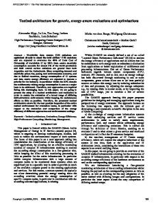
round 0
plain text
key
Fig. 1 Outline of the 128-bir key AES encryption algorithm
240
IEE Proc.-Comput. Digit. 'Tech., Vol. 150, No. 4, July Z W 3
Fig. 2 Outline of encqyddecrypt Rijndael 128-bir key design
clock cycles respectively. Similarly to the input data, the encrypte4decrypted data is output in 32-hit blocks over four clock cycles. Many applications will only require the use of one of the three possible key sizes. Therefore, the key length is a generic input of the design [4]. Having all three key length design options available will only increase the area overhead unnecessarily. However, if a different key size is required, the core does not need to he re-designed, the generic key-length input value is simply changed and the design re-synthesised. Both encryption and decryption are supported. The main distinction between encryption and decryption-only designs is that the values of the look-up tables (LUTs) used to implement the SuhBytes transformation differ. One method to provide both encryption and decryption capabilities involves the addition of two LUTs or ROMs, which are used to initialise the SuhBytes transformation ROMs, one containing initialisation values for the LUTs required during encryption and the other containing the values required during decryption [SI. However, this method incurs a latency each time there is a change of mode from encryption to decryption and vice versa. In the currently described architecture the change from encryption to decryption of data can occur on-the-fly. Since the architecture is iterative, the round and inverse round transformations can both he included, incurring only a small area overhead. Fig. 2 pictorially describes the encrypt/ decrypt Rijndael design for a key length of I28 hits. The load counter loads the data and key over four cycles in 32-bit blocks. Similarly, the output counter outputs the encryptedldecrypted data over four cycles. The 128-key counter controls the timing of the overall design. The 192-hit and 256-hit key designs will he similar to that shown in Fig. 2. In these designs the load counter loads the key over six and eight cycles respectively and the data over four cycles. 192-key and 256-key counters are also required to control the timing in these circuits. In the design of the AES round [3], the SubBytes transformation is implemented using 16 8-bit to 8-bit LUTs or eight BRAMs when the design is targeted towards a Xilinx Virtex device. Similarly the InvSuhBytes transfomation in the inverse round is implemented utilising 16 LUTs. An iterative process is used to access the round or inverse
round for 9, 11 or 13 cycles depending on the key length, analogous to the algorithm’s 9, I 1 or 13 typical rounds. On the loth, 12th or 14th cycle, again depending on the key length, the MixColumns and InvMixColumns transformations are bypassed corresponding to the final round and inverse final round respectively. The 128-bit key schedule design for encryption [14] also uses an iterative process. When using a 128-bit key, 40 4-byte vectors or words are created during key expansion. Only every fourth word is passed through the s-box, which is implemented as four LUTs using two BRAMs. Since each round only requires four words at a time, it is possible to use an iterative design to access the same BRAMs every clock cycle. Similarly, in the 192-bit and 256-bit key schedules only two BRAMs are required in their design. It is assumed that the same key is used during a data transfer session. The key schedule design for decryption achieves on-the-fly generation of the decryption round keys, as described in Section 4.1. Similarly to the key schedule design for encryption it also utilises two BRAMs in its 128-bit, 192-hit and 256-bit key schedule implementations. Each design requires a total of 40 LUTs or 20 BRAMs, eight in the round, eight in the inverse round, two in the encryption key schedule and two in the decryption key schedule.
4.1 On-the-fly generation of decryption rounds keys During decryption, the AES key schedule remains unchanged. The round keys created during key expansion are simply utilised in reverse order as depicted in Fig. 3. Typically, during the decryption process it is therefore necessary to wait at least 10, 12 or 14 clock cycles, depending on the key length, for the round keys to he created before decryption can commence. Registers can be used to store the keys until they are required. Altematively, the round keys could he pre-computed and stored in the memory. However, on-the-fly calculation of the round keys for decryption can be achieved. If the final Nk words created during key expansion in the encryption process are utilised as the cipher key during decryption, the round keys required for decryption can be created as they are needed by the
... ... md key10
md
md
key9
key8
md key7
md
md
key 1
key 0
Fig. 3 Round key utilisation in decvpyprion procesr f o r a 128-bit cipher key IEE Proc.-Comput. Dwir Tech., Vol. 150. No. 4, July 2003
24 1
when N, = 4 or 6: for(;= w(N,+ 1) -1; i>w(N,+l)-Nk i--) ~
InvCipherKey[4'(hb.(N,+ 1)-1-0],InvCipherKey[N;N, + 1)-14+1], InvCipherKey[4*(N,'(N, + l)-ld)+21, InvCipherKev[4'(N,'(N, + l).l-i)+3];
W[q = (
f o r ( ; = Nb'(N,+ l).l; i 2 NI: i-) (
temp = W[i - I]; if ( iX
1
4== 0)
temp = SubWord(RoWard(temp)) XOR Rcon(il4):
WkNJ = Wr]XOR temp;
when Nk = 8: lor(i= Nb'(N,+l)-l;i2N