1
Graphene transistors for bioelectronics Lucas H. Hess, Max Seifert, and Jose A. Garrido Abstract—This paper provides an overview on graphene solution-gated field effect transistors (SGFETs) and their applications in bioelectronics. The fabrication and characterization of arrays of graphene SGFETs is presented and discussed with respect to competing technologies. To obtain a better understanding of the working principle of solution-gated transistors, the graphene-electrolyte interface is discussed in detail. The in-vitro biocompatibility of graphene is assessed by primary neuron cultures. Finally, bioelectronic experiments with electrogenic cells are presented, confirming the suitability of graphene to record the electrical activity of cells. Index Terms—Bioelectronics, Graphene
I. INTRODUCTION
A
MAJOR challenge in the field of bioelectronics is the advancement of neural prostheses that allow restoring damaged abilities such as hearing[1] and vision, [2] or can help to find solutions for treating motor disabilities[3] or brain pathologies.[4] For this, it is essential to develop suitable interfaces between the biological system, such as the cochlea in the ear or the retina in the eye, and electronic devices. While the intermediate signal processing can be done easily with standard microprocessors, an efficient signal transfer from the electronics to the nervous systems, and vice versa, remains challenging. Commercially available technologies are mostly based on micro electrode arrays (MEAs) made from silicon or metals. [1, 2, 5] MEA-based devices already have shown partial success in reconstituting hearing and vision, or in treating neural disorders. However, the performance of such implants, including long-term stability, is far from being satisfactory and has to be largely improved. In addition, MEA devices have an intrinsic poor spatial resolution, which is related to the rather large electrode impedance.[6] Arrays of field effect transistors (FETs), on the other hand, have also been demonstrated for recording the electrical activity of nerve cells and tissue, [7, 8] and offer certain advantages with respect to MEAs such as the intrinsic amplification capabilities of FETs. Further, signal-to-noise ratios can be considerably enhanced if submicron FETs are used for recording. Finally, since FETs can be fabricated by standard semiconductor technology the production of high density structures is relatively easy, which has been used to demonstrate the
Manuscript received July 6, 2012. This work was supported by the European Union through the project NeuroCare, the German Research Foundation (DFG) in the framework of the Priority Program 1459 “Graphene”, and the Nanosystems Initiative Munich (NIM).
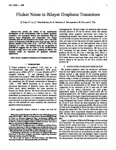
Fig. 1: Concept for a retinal implant. An image is acquired by a camera which is mounted to eyeglasses. After processing, the information is transferred to a retinal implant which stimulates nerve cells to transmit the signal to the brain.
recording of cell activity with unprecedented spatial resolution.[9] However, the presently used FETs platforms suffer from some major drawbacks, which are not only related to an imperfect technology but are also inherent to the materials that are employed. One of the problems is the poor stability of many materials in the harsh biological environment. For example, devices fabricated from the ubiquitous semiconductor silicon are subject to stability problems in aqueous environments.[10, 11] This does not only result in a decreased performance of the sensor but may also damage the surrounding tissue. Furthermore, to obtain high performance electronic devices exhibiting high charge carrier mobilities and low electronic noise, which are required for a high signal-to-noise ratio, it is necessary for classic semiconductors to build devices on the basis of highly crystalline substrates or even single-crystals. However, such good crystalline properties come hand in hand with mechanical characteristics like high rigidity and sharp edges. In biological systems, it is known that rigid and sharp prostheses can induce scarring around the device making it inoperative and damaging the surrounding tissue. Thus, it is a major challenge to develop sensors from a chemically stable material which should exhibit good electronic properties allowing at the same time the fabrication of small, flexible devices. Graphene complies with all of these requirements.[12] Built up only from sp2-hybridized carbon The authors are with the Walter Schottky Institut, Technische Universität München, Am Coulombwall 4, 85748 Garching, Germany (e-mail:
[email protected];
[email protected];
[email protected]).
2
Material Silicon[18] Diamond[18] AlGaN/GaN[18] Graphene[18]
Charge carrier mobility µ (cm2/Vs) 450 120 1200 4000
TABLE I OVERVIEW OF MATERIALS FOR SGFETS Transconductance gm/UDS Interfacial capacitance Cint mS/V (µF/cm2) 0.35 2 0.32 2
0.20 0.29 0.51 5
Biocompatibility
Flexibility
0[8] +[22] +[23] +[24]
0[21] +[20]
Table I: Properties of field effect transistors prepared using different material systems which have been proposed for bioelectronic applications. Graphene has both high charge carrier mobilities and a high interfacial capacitance which results in a high transconductive sensitivity. Additionally, graphene is chemically very stable, biocompatible, and is fully compatible with flexible technology
atoms, whose interatomic bond is one of the strongest in nature, graphene shows a very high chemical stability even in harsh biological environments. As will be discussed later, this stability results in an excellent biocompatibility. In addition, the band structure of graphene results in outstanding electronic properties.[13] Charge carriers close to the charge neutrality point, also referred to as Dirac point, behave like quasi-relativistic particles, which largely reduces scattering and gives rise to extremely high charge carrier mobilities. Even at near-room temperature, values of more than 105 cm2V-1s-1 [14] can be reached with exfoliated graphene, outnumbering other semiconductors which have been so-far used for similar applications. Furthermore, the chemical properties of graphene allow the fabrication of transistors without any solid dielectric.[15, 16] As a result, interfacial capacitances of several µFcm-2 can be obtained, which is almost one order of magnitude higher than for traditional semiconductors with a fairly stable dielectric.[17] Consequently, graphene shows significantly higher transconductive sensitivities than other materials.[18] Moreover, the fact that graphene is only one atomic layer thick and can be transferred to almost any arbitrary substrate – including thin polymer films – allows the fabrication of high performance fully flexible transistors.[19, 20] Table I shows a comparison of the relevant properties of FETs based on graphene and other commonly used semiconductor materials. Although graphene technology is still in its infancy, graphene-based FETs already offer advantages when compared to the other competing technologies. In terms of biocompatibility, graphene exhibit a similar performance than diamond[22] and AlGaN/GaN,[23] whereas silicon devices require additional encapsulation layers to improve their stability.[25] Some materials, such as carbon nanotubes, also allow the fabrication of sensitive solution-gated transistors,[26] but their biocompatibility is still controversial.[27] Manufacturing flexible devices is not possible with singlecrystalline diamond or AlGaN/GaN heterostructures and strongly deteriorates the electronic properties for silicon.[21] In contrast, graphene proved to be chemically stable and the feasibility of high-quality flexible transistors has already been demonstrated. [19,20] Figure 2 shows a schematic of a neuroelectronic hybrid circuit based on graphene devices. Cells are grown on top of an array of graphene transistors, which can be used for the
bidirectional communication with cells. In fact, the rather large interfacial capacitance of graphene SGFETs offers a more effective capacitive stimulation than Si-based SGFETs can provide. Thus, the graphene transistors can be used to either stimulate or record signals from cells. Recordings of the electrical activity of electrogenic cells using graphene transistors have been reported recently,[28,29] based on a configuration similar to the one shown in Figure 2, confirming the enormous potential of graphene SGFETs for bioelectronic applications. In this paper, we summarize our work on graphene solutiongated transistors. Firstly, the basic working principle of graphene SGFETs is explained, including the fabrication and basic characterization. Then, the graphene/electrolyte interface is described in more detail to better understand the electrolytegating of graphene. Thereafter, the electronic requirements for semiconductor biosensors are discussed and the suitability of graphene SGFETs for these applications is assessed. In the final chapter, graphene SGFETs are tested in biological systems assessing their biocompatibility and demonstrating recordings of cell action potentials.
Fig. 2: Neuroelectronic circuits and interfaces. For advanced neuroprostheses as well as for in-vitro neuronal networks studies, bidirectional communication with neurons is necessary, i.e. signals need to be transferred to and from the neurons to the electronics (upper part). Here, cells are grown on graphene transistors, which allow recording action potentials from the cells (lower part).
3 II. FABRICATION AND TECHNOLOGY A. CVD growth and transistor fabrication High-quality graphene can be fabricated by several methods such as mechanical exfoliation, thermal decomposition of silicon carbide and chemical vapor deposition (CVD). Graphene sheets produced by mechanical exfoliation are very restricted in size (40000 cm2V-1s-1.[35] Furthermore, it can be transferred to any substrate including flexible materials. To grow graphene by CVD, a copper foil is introduced into a furnace(see Figure 3a) and is heated to 1000°C under hydrogen flow to remove the native copper oxide. After this etching step, the gas flow is changed to a methane/hydrogen mixture, which provides the carbon source for the growth of graphene on copper. Subsequently, the graphene has to be removed from the copper and transferred to an insulating substrate. As depicted in Figure 3b, a layer of poly(methyl 2-methylpropenoate) (PMMA) is spin-coated on the graphene/copper stack to provide mechanical stability to the graphene layer. This stack is placed on the surface of an iron(III)chloride solution, which etches the copper under the graphene. After diluting, the graphene/PMMA layer is fished on the final substrate and the PMMA is removed by dissolving it in solvents. A final annealing step can be used to further remove residues from the PMMA. Then, the graphene is patterned by optical lithography and an oxygen plasma etch is used in order to define the active area of the devices (Figure 3c). The ohmic drain and source contacts are prepared by gold evaporation and etching in a KI/I2 solution. Finally, a structured layer of chemically stable SU8 photoresist is applied to the sample to protect the gold contacts from the electrolyte and to prevent leakage currents. After a final annealing step, the devices are wire-bonded to a chip-carrier. The bonding wires are covered with silicone glue to insulate them from the electrolyte. In order to have spatial resolution for the cell experiments, several transistors are fabricated in one array. The optical micrograph in Figure 3d shows one half of a 4×4 transistor
Fig. 3: Fabrication of graphene SGFETs. a) Graphene films are grown on copper foil by CVD in a furnace at 1000°C under a flow of methane and hydrogen. b) With the help of a protective PMMA layer, the copper is etched away and the graphene is transferred to an insulating substrate. c) To fabricate the transistors, the graphene is etched with oxygen plasma and contacted via gold leads. For operation in an electrolyte, the metal is insulated with a chemically resistive resin. d) Optical micrograph of a transistor array and close-up of a single transistor. The graphene cannot be seen directly and is indicated with a box. The scale bars are 50 µm.
array. For cell experiments, it is important that the size of the transistors, i.e. its gate area, is similar to the cell size. Large transistors, which are only partially covered by the cell, result in a poor gating of the device. In our experiments, typical
4 transistors have a length of 10 µm and a width of 20 µm. B. Basic characterization For the characterization in electrolyte, the transistor array is immersed in a solution containing 5 mM phosphate buffered saline (PBS) and adjusted to an ionic strength of 100 mM with KCl. The gate voltage UGS is applied between the source contact of the transistors and a Ag/AgCl reference electrode in the
Fig. 4: Current vs. voltage characteristics of a graphene SGFET. a) The drain-source current shows a linear dependence on the drain-source voltage. No saturation can be observed within the applied UDS voltages. b) When plotted against the gate-source voltage, the current shows a minimum and increases continuously afar from this point. The shown transistor is 20 µm wide and 10 µm long.
solution. When a voltage is applied between the drain and the source contacts of a transistor, a current can be observed. This current is proportional to the applied drain-source voltage UDS (see Figure 4a) and can be modulated with the gate voltage. At a certain UGS, the current shows a minimum value and increases almost linearly afar from this point (see Figure 4b).
valence band and the charge density increases. For EF above UD, the conductivity is due to electrons in the conduction band, whose density can be modulated similarly. The voltage at which the Dirac point is reached in our experiments depends on several factors, such as the absolute electrochemical potential of the reference electrode and the work function of graphene. As both have similar values (4.6 eV [37, 38] and 4.5 eV [39], respectively), the expected Dirac voltage would be much closer to zero than the observed values between 0.3 V and 0.4 V. The reason for this difference is most likely due to the p-type doping of the graphene induced by its environment (such as the underlying substrate) or surface contamination (adsorbed water or remaining contamination from the device processing).[40] We have found a similar doping level for a variety of substrates including sapphire, silicon dioxide, and polyimide films, whereas n-type doping was observed for SGFETs prepared using graphene grown on SiC. [18] Hall effect experiments employing solution-gated van-derPauw structures and Hall bars can be used to investigate the electrolytic gating of the carrier density in graphene.[36] Figure 6a shows the sheet conductivity as a function of the gate voltage obtained from these experiments revealing the expected Vshape curve typical of ambipolar transport, similar to the transistor curves shown in Fig. 4. Regarding the charge carrier density, a positive charge is observed for gate voltages below the Dirac point. As shown in Figure 6, the density of positive charge carriers decreases when UGS approaches the Dirac point. For gate voltages higher than UD, the sign of the charge carriers is inverted and their density increases again. From the sheet conductivity and the charge carrier density, it is possible to extract the mobility of the carriers in the graphene sheet (see Figure 6b). Mobilities higher than 8000 cm2V-1s-1 can be observed close to the Dirac point. Increasing the carrier density results in a decrease of the mobility, which reaches values of 1100 cm2V-1s-1 and 800 cm2V-1s-1 for holes and electrons, respectively, for a carrier density of 5×1012 cm-2. The observed dependence of the mobility with the carrier density is consistent
III. GRAPHENE-ELECTROLYTE INTERFACE A. Electrolyte Gating The conductivity gating observed in Figure 4 can be explained by a simple model describing the grapheneelectrolyte interface, as shown in Figure 5.[36] As the potential level of the Ag/AgCl electrode is fixed with respect to the vacuum level, applying a voltage between this electrode and the graphene shifts the position of the Fermi level in the graphene, which controls the number of free carriers induced electrostatically. When the Fermi level reaches the Dirac point, i.e. the energy where conduction and valence band meet, the conductivity in the graphene film shows its minimum value. The voltage at which this is observed is referred to as Dirac voltage UD. For EF below UD, the majority charge carriers are holes in the graphene valence band. When the gate voltage is further decreased, the Fermi level is shifted deeper into the
Fig. 5: Electrolyte gating of graphene. By applying a voltage between the graphene and the reference electrode, the Fermi level in the graphene can be shifted. Hereby, the conductivity can be modulated and the type of charge carriers can be changed between electrons (a) and holes (b).
5 However, close to the interface, the above approximation does not hold. Very close to hydrophobic surfaces such as graphene, the structure of the water itself changes drastically.[44] As shown by molecular dynamics simulations,[45] the density of water decreases strongly at the surface resulting in a so-called hydrophobic gap between the solid and the electrolyte (see Fig. 7). In this gap, the effective dielectric constant is much smaller than in bulk water resulting in a large potential drop at the interface. The graphene/electrolyte interface was simulated with the commercially available Poisson-Schrödinger solver nextnano3.[46] This software self-consistently simulates the electronic structure of semiconductor materials as well as the potential and ion distribution in the electrolyte. On the electrolyte side, the above mentioned hydrophobic gap was considered with the help of a non-uniform dielectric constant of the water close to the surface which was obtained from Fig. 6: Electrolyte-gated Hall effect characterization. a) Sheet molecular dynamics simulations. [45] The ion distributions conductivity (black squares) and charge carrier density (red circles) were calculated with a Poisson-Boltzmann model which was are modulated with the gate voltage. At 0.4 V, the minimum extended by spatially varying potentials of mean force (PMF) conductivity, i.e. Dirac point, is reached and the sign of the majority for each ion; such PMFs are introduced to prevent the carriers changes. b) Carrier mobility versus carrier density, unphysical situation of ions approaching the surface infinitely revealing that holes exhibit higher mobilities than electrons. The close.[45] mobility-density dependence suggests that carrier scattering is Figure 8 shows the charge carrier density obtained dominated by surface polar phonons.[41] Inset: Combined device experimentally as well as the results from the simulations. A with 8 transistors surrounding a van-der-Pauw structure. good agreement is seen for the hole regime (UGS-UD