Hindawi Publishing Corporation e Scientific World Journal Volume 2014, Article ID 131568, 9 pages http://dx.doi.org/10.1155/2014/131568
Research Article Hardware Implementation of 32-Bit High-Speed Direct Digital Frequency Synthesizer Salah Hasan Ibrahim,1,2 Sawal Hamid Md. Ali,2 and Md. Shabiul Islam3 1
Department of Electronics, College of Engineering, Diyala University, Baqubah, Diyala 32001, Iraq Department of Electrical, Electronics & System Engineering, Faculty of Engineering, Universiti Kebangsaan Malaysia (UKM), 43600 Bangi, Malaysia 3 Institute of Microengineering and Nanoelectronics (IMEN), Universiti Kebangsaan Malaysia (UKM), 43600 Bangi, Malaysia 2
Correspondence should be addressed to Salah Hasan Ibrahim;
[email protected] Received 4 February 2014; Revised 13 March 2014; Accepted 29 April 2014; Published 2 June 2014 Academic Editor: Robert Adams Copyright © 2014 Salah Hasan Ibrahim et al. This is an open access article distributed under the Creative Commons Attribution License, which permits unrestricted use, distribution, and reproduction in any medium, provided the original work is properly cited. The design and implementation of a high-speed direct digital frequency synthesizer are presented. A modified Brent-Kung parallel adder is combined with pipelining technique to improve the speed of the system. A gated clock technique is proposed to reduce the number of registers in the phase accumulator design. The quarter wave symmetry technique is used to store only one quarter of the sine wave. The ROM lookup table (LUT) is partitioned into three 4-bit sub-ROMs based on angular decomposition technique and trigonometric identity. Exploiting the advantages of sine-cosine symmetrical attributes together with XOR logic gates, one subROM block can be removed from the design. These techniques, compressed the ROM into 368 bits. The ROM compressed ratio is 534.2 : 1, with only two adders, two multipliers, and XOR-gates with high frequency resolution of 0.029 Hz. These techniques make the direct digital frequency synthesizer an attractive candidate for wireless communication applications.
1. Introduction Direct digital frequency synthesis (DDFS) systems with highspeed frequency hopping function, low power consumption, high frequency resolution, and small chip area are in a great demand for DDFS applications especially in wireless communications and radar systems. DDFS systems have low noise and high frequency resolution compared with phase lock loop [1]. The DDFS output frequency (𝐹out ) is given by 𝐹out = (
FCW ) ∗ 𝐹clk , 2𝑁
(1)
where 𝐹clk is clock frequency, FCW is a frequency control word, and 𝑁 is the phase accumulator width. Pipelining technique is defined as a technique that partitioned the given task into a number of subtasks that need to be performed in a sequence. The pipelining technique is used in [2–4] to increase the throughput of the output frequency. However, this technique also increases the power consumption and chip area. The gated clock technique was applied to the
pipeline phase accumulator (PA) in [5] to reduce the number of registers without performance degradation. A parallel adder based on progression-of-states technique was combined with the pipelining technique in [6, 7], for high-speed, low power pipelined parallel PA. The pipelined accumulator with parallel adder technique was proposed in [8]. In this paper, two blocks of parallel 16-bit ripple carry adder (RCA) are designed based on the progression-of-states technique with two pipelining stages. DDFS spectral purity depends on the number of the phase output bits used for addressing the ROM. Therefore, the higher spectral purity required, the bigger ROM size needed. The quarter wave symmetry in [9, 10] was applied as a simple technique to reduce the ROM size, storing only quarter (0 : 𝜋/2) of the sine wave bits and using the two most significant bits (MSB) to generate the full sine wave (2𝜋). Quarter wave symmetry together with an angular decomposition method based on trigonometric identity was used in [11–13] to compress the ROM size by partitioning the ROM into three sub-ROMs. This technique was also
2
The Scientific World Journal
8
8
8
8
8-bit reg.
8-bit reg.
8-bit reg.
8-bit reg.
8-bit reg.
8-bit reg.
8-bit reg.
+
8-bit reg.
8-bit reg.
+
8-bit reg.
+
+
8-bit reg.
8-bit reg.
8-bit reg.
8-bit reg.
8-bit reg.
Figure 1: The conventional 32-bit pipelining phase accumulator.
used in [14], where the ROM is partitioned into two ROMs, namely, coarse and fine ROMs, to obtain the quadrature outputs, sine and cosine values. The author suggested several DDFS systems implemented with different types of FPGA kit boards and compared them with an ASIC based approach. The polynomial approximation method was used in DDFS design to optimize the spurious-free dynamic range (SFDR). This method was used by Ashrafi and Adhami in [15] to determine the upper bound of the SFDR using piecewise polynomial interpolation. Fourier series was used to establish a linear relationship between the coefficients of the interpolating polynomials and the frequency spectrum. This method can be used in any kind of DDFS to maximize the SFDR. De Caro et al. proposed a dual-slope technique in [16] to optimize the piecewise linear approximation for the phase to sine mapping. This technique improves the spectral purity and ROM size. The stored values of the two quarters (𝜋/4) sine and cosine sub-ROMs, with 3 MSB bits and mapper, are required to accomplish the quarter phase to sine mapping and produce quadrature output from the DDFS. In [17], De Caro et al. proposed another DDFS architecture which is based on piecewise linear approximation technique with nonuniform segment length to the input of three groups of multiplexer. This technique can maximize the SFDR and reduce the size of the coefficients ROM. This paper presents a high-speed DDFS system with pipelined PA based on modified parallel BK adder and gated clock technique. The ROM was resized by applying the quarter-wave symmetry technique in one quarter of the sine wave, and an angular decomposition technique based on trigonometric identity has been applied to compress the quarter ROM LUT. Based on these techniques, the quarter ROM LUT was partitioned into three sub-ROMs (𝐴, 𝐵, and
𝐶). The proposed architecture improves the speed of the DDFS and reduces the size of the ROMs.
2. The Gated Clock and Parallel Pipelining Technique for Phase Accumulator The modified parallel BK adder based on the progression-ofstates technique combined with gated clock technique was used in the proposed design of the PA. The frequency resolution (𝐹Res ) of DDFS is determined by the clock frequency (𝐹clk ) and the number of 𝑁 input bit of the PA as depicted by 𝐹Res =
𝐹clk . 2𝑁
(2)
For high frequency resolution, it is preferable to design a PA with large FCW bits input. However, a large ROM size is required to implement all the 2𝑁 bits of phase accumulator output. Due to this reason, a part of the MSB phase output is used to address the phase to amplitude converter or ROM lookup table while maintaining high frequency resolution. The pipeline technique was used to increase the throughput of the accumulator, and this throughput will double with the number of pipeline stages, as shown in Figure 1. The number of registers increases with the number of pipeline stages, which leads to high power consumption. Therefore, in this design, a gated clock technique was used to reduce the number of preskewing registers while preserving high-speed operation. In this technique, D flip-flops (DFFs) were used to connect each row of the pipeline stages with FCW input. These registers are clocked by the pipelined pulses with one clock cycle based on the shifted clock pulses as shown in Figure 2(a). Considering that the phase accumulator input bits are 𝑁, the PA was partitioned into 𝐿
The Scientific World Journal Vcc
3
DFF
3 Td
2 Td B
1 Td A
K Set DFF Fclk
DFF
IN [7 : 2] LOW [1 : 0]
C
DFF
+
OUT X(T + 4) [7 : 0]
C 1
2
3
4
5
6
7
8
9
B A
1
2
3
4
5
6
7
8
1
2
3
4
5
6
7
8
1
2
3
4
5
6
7
8
+
9 IN [7 : 0] LOW [1 : 0]
Clk
IN [7 : 1] LOW [0] +
9
(a)
8-DFF
+
OUT X(T + 3) [7 : 0] OUT X(T + 2) [7 : 0]
OUT X(T + 1) [7 : 0]
(b)
Pipelined PA output Parallel adder
X2
X3
Multiplexer
X4
X1
1
2
3
Clk/4
4
Clk
(c)
Figure 2: (a) The gated clock technique, (b) parallel adder based on progression-of-states technique, and (c) pipelined PA output.
stages with B DFFs in each stage. The number of the DFFs, 𝐾 for preskewing registers, is given by 𝐾=
(𝑁 ∗ (𝐿 + 1)) . 2
(3)
By applying the gated clock technique on the proposed design, the number of DFFs is given by 𝐾 = 𝑁 + 𝐿.
(4)
As a result, with the gated clock technique, the numbers of preskewing registers have been reduced from 80 to 36 corresponding to 53.7% reduction. Figure 2(b) shows the operation of the parallel adder. Four adders calculate the holding constant of 8-bit input word within four clock cycles. Holding the FCW for four clock cycles limits the update rate of the frequency input word but does not cause any glitch, because the four adders will steadily increase the accumulator output four times. Assume that FCW is 𝑁 and the parallel adder output is 𝑋 at the 𝑇th clock time. The parallel adder’s outputs are given as follows: 𝑋 (𝑇 + 1) = 𝑁 + 𝑋 (𝑇) , 𝑋 (𝑇 + 2) = 𝑋 (𝑇 + 1) + 𝑋 (𝑇) = 𝑁 + 𝑋 (𝑇) + 𝑋 (𝑇) = 𝑁 + 2𝑋 (𝑇) , 𝑋 (𝑇 + 3) = 𝑋 (𝑇 + 2) + 𝑋 (𝑇) = 𝑁 + 3 𝑋 (𝑇) , 𝑋 (𝑇 + 4) = 𝑋 (𝑇 + 3) + 𝑋 (𝑇) = 𝑁 + 4𝑋 (𝑇) . (5)
The result of the fourth adder is set as a feedback to the second input for all the four adders. To generate the second output [𝑋(𝑇+2)] and fourth output [𝑋(𝑇+4)], the 𝑁 bit is shifted up by removing one and two bits of the FCW input and replacing them with the one and two bits from the lower pipelining stage, respectively, before they are added. The 𝑋(𝑇+2) output and 𝑋(𝑇) output are used to generate 𝑋(𝑇 + 3). This operation made the frequency tuning word held constant for four clock cycles without causing any imperfections in the PA output. The partitioned clock cycles (𝐶𝑙𝑘/4) make the multiplexers choose one of the results at the output of the PA to overcome the holding time on the parallel adders as illustrated in Figure 2(c).
3. Phase Accumulator Architecture The proposed phase accumulator architecture based on the modified parallel BK adder and the gated clock technique with pipelining stages is shown in Figure 3. The output of the PA is a truncated 14-bit value that is achieved from the 8 and 6 bits of the top and second pipelining stages, respectively. The 32-bit FCW input is sufficient to obtain 0.029 Hz frequency resolution from the 125 MHz clock frequency of Cyclone III FPGA kit board (𝐹Res = 125 × 106 /232 = 0.029 Hz). 3.1. Modifying Brent-Kung Adder. The BK adder is fast, and all carries are computed simultaneously through a binary tree of “BK” cells as shown in Figure 4(a).
4
The Scientific World Journal
+
IN [7 : 0] IN [7 : 1] LOW [1 : 0]LOW [0]
+
IN [31 : 24]
8-bit reg. ] [9 : 8 IN [15 : 8]
4-DFF
24-bit reg. 8-bit reg. 6-bit reg.
4-DFF
8 8
+
32-bit reg.
8
6 OUT X4
6-DFF
6 OUT X3
6-DFF
6 OUT X2
6-DFF
24-bit reg.
18-bit reg.
24
6 OUT X1
6-DFF
MUX 8 4×1 14 OUT [31 : 18]
MUX 6 4×1
Clk
8-bit reg.
Clk/4
Clk/4
]
DFF
[1 : 0
DFF
8-bit reg. 8-bit reg.
+
8-bit reg.
8
8-DFF
+
IN [7 : 0] IN [7 : 1] LOW [1 : 0] LOW [0]
+
IN [23 : 16]
DFF
+
+
+
8-bit reg.
DFF
Set
IN [7 : 2] LOW [1 : 0]
8 OUT X4 8-DFF 8 OUT X3 8 + 8-DFF 8 OUT X2 32 8 8-DFF 8 OUT X1 8 8-DFF 8
MUX
+ 8-DFF
[17 : 16]
IN [7 : 2] LOW [1 : 0]
K Clk
IN [7 : 0]
8-bit reg.
DFF 8-bit reg.
+
Clk
Clk
Figure 3: Pipelined phase accumulator with parallel adder based on modifying Bren-Kung adder and gated clocking technique.
BK cells compute the carry for two or more of full adder (FA) cells, and they are calculated as a sum of 𝐺 and 𝑃 cells [23, 24]. The arithmetic operation is given by
modification of the 8-bit BK adder is shown in Figure 4(b). The sum and carry out of the modified 8-bit BK adder are shown in
BK = 𝐺 + 𝑃,
𝑆0 = 𝑝0 ⊕ 𝑐in ,
𝐺 = 𝑔 + 𝑝 ⋅ 𝑔 ,
(6)
𝑆𝑁⋅⋅⋅1 = 𝑝((𝑁−1)⋅⋅⋅1) ⊕ 𝐶((𝑁−1)⋅⋅⋅1) ,
(8)
𝑃 = 𝑝 ⋅ 𝑝 ,
𝐶out = 𝑔𝑁 + 𝑝𝑁 ⋅ 𝐶𝑁.
where 𝑔 𝑔 , 𝑝 𝑝 are higher and lower generate and propagate functions, respectively. The 𝑝 is a propagate function (𝑝𝑖 = 𝑥𝑖 ⊕ 𝑦𝑖 ) and 𝑔 is a generate function (𝑔𝑖 = 𝑥𝑖 ⋅ 𝑦𝑖 ). The general prefix addition algorithm is explained by Zimmermann in [25]. By adding the carry input 𝐶in in the prefix structure with some modifications, the prefix structure can be used in pipelining-based adder design. This approach is used in BK adder fast carry computation. However, in this paper, a modification is proposed to the BK adder so that it can be used in pipelining architecture. The proposed modification is by removing the operation of the 𝑔0 , and the carry out of the first bit 𝐶1 can be achieved by a 2-1 multiplexer. The input to this multiplexer is 𝑥0 and 𝐶in while 𝑝0 is the select input and the output is 𝐶1 . The operation of the multiplexer is given by
3.1.1. Comparison of Different Adder Architecture. An adder is a key element of the pipelining PA design, and a fast adder improves PA performance. Parallel-prefix adder tree structures such as Sklansky [26], Kogge-Stone adder [27], BK [23], and Beaumont-Smith [28] have been used in pipelining accumulator design for high-speed operation. A comparison has been made between conventional adder and several parallel-prefix adders for 12-bit, 18-bit, 24bit, and 32-bit operations. The PA designs were coded in Verilog HDL and verified in Cyclone III FPGA kit board. Prior to that, all the designs were simulated by using ALTERA Quartus II. The comparison result is shown in Figure 5. From the figure, it can be seen that BK adder performs relatively faster, especially for high number of bits.
𝐶1 = (𝑝0 . 𝑐in ) + (𝑥0 . 𝑝0 ) ,
(7)
where 𝐶1 is the carry out, 𝑝0 is the propagate function, 𝐶in is the carry input, and 𝑥0 is the first bit input. The proposed
4. ROM Lookup Table Design ROM LUT or phase-to-amplitude converter (PAC) is a memory storage address for DDFS, which is used to convert
The Scientific World Journal
5 x1 y1
···
P·g P·g P·g P·g P·g P·g P7· g7 p6· g6 p5· g5 p4· g4 p3· g3 p2· g2 p1· g1 P·g
BK
BK
BK
x7 y7
pg
P·g P·g P·g P·g P·g P·g P·g P7 · g7 p6· g6 p5· g5 p4· g4 p3· g3 p2· g2 p1· g1
p0 g0
BK
BK P6
P5
·p
C1
BK
BK
Critical path
p Cin
BK Critical path BK
BK
P7
BK
BK
BK
BK
BK
···
BK
BK
x0 y0
x1 y1
x0 y0
MUX
x7 y7
BK P4
P3
S
S
S
S
S
S7
S6
S5
S4
S3
BK P2 S
S2
P1
P0
P7
BK P6
P5
BK P4
BK
P3
P2
Cin
C1
S
S
S
S
S
S
S
S
S
S
S1
S0
S7
S6
S5
S4
S3
S2
S1
S0
(a)
(b)
Figure 4: Block circuit diagram of conventional Brent-Kung adder (a) and (b) modifying Brent-Kung adder.
400 P-2
350 300 250
4
sine B sin B 28 × 4 Bit ROM
C 4
sin C sine C 24 × 4 Bit ROM
B
11
+
11 cos A
C sine A/cos A sine A 24 × 11 4 Bit ROM
cos A
Maximum operation frequency (MHz)
450
11 +
cos A × sin B 11
11 sin out
cos A × sin C
200
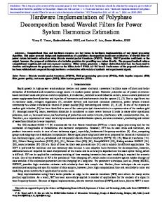
Figure 6: Architecture of compressed ROM LUT design. 150 100 10
15 CLA RCA Brent-Kung
20 25 Number of bits
30
35
Kogge-Stone Sklansky Beaumont Smith
Figure 5: Comparison result of maximum operating frequency (𝐹Max ) for phase accumulator design with CLA, Brent-Kung, KoggeStone, Sklansky, Beaumont-Smith, and RCA adders.
the phase signal into an amplitude sine wave signal. Highaccuracy output signal for DDFS requires a large number of LUT. The ROM size exponentially increases with increasing number of bit inputs. The designer’s challenge is a tradeoff between reducing the ROM size while maintaining high performance (high resolution, high speed). Quarter-wave symmetry technique is used to resize the ROM in the proposed DDFS design to store only one quarter (0 : 𝜋/2) of
the sine waveform and two most significant bits (MSB) from the phase accumulator are used to reconstruct the full sine wave. From these two MSBs, one of them is used to determine if the sine amplitude is increasing or decreasing and the other one is used to determine its sign. The phase output is directly used in the first and third quarter while the inverse values of the phase output are used in the second and fourth quarters. This requires 2’s complement when the phase is between (𝜋 : 2𝜋) and is achieved by adding full adder at the output gate to accomplish the full sine wave value. To save power and achieve a smaller area design, the 1/2 LSB offset is added to the stored memory address of sub-ROMs. This offset removes the full adder component from the 2’s complement of the proposed design. The angular decomposition technique based on trigonometric identity is one of the best techniques to reduce the quarter ROM LUT size. The quarter ROM LUT was partitioned into three (𝐴, 𝐵, and 𝐶), such that 𝐴 < (𝜋/2),
6
The Scientific World Journal
MSB1 DDF
MSB2
sine A/cos A 24 × 11 = 176 bit ROM
cos A +
P P-2 Register
1st comp.
sine B 24 × 8 = 128 bit ROM sine C 24 × 5 = 80 bit ROM
Fclk
sin B
cos A
Frequency control N Adder word
sin A
+
Reg.
P-2
1st comp.
DAC Fout /LPF
sin C
Figure 7: The block diagram of the final design of high-speed DDFS.
Figure 8: Signal tap logic analyzer of FCW input (in hexadecimal), the sawtooth PA output, and half and full amplitude waveform.
𝐵 < (𝜋/2) ∗ (1/2𝐴 ), and 𝐶 < (𝜋/2) ∗ (1/2𝐴+𝐵 ), with the same approximations based on trigonometric identity. According to the trigonometric relation, the sine wave function is given in sin (𝐴 + 𝐵 + 𝐶) = sin (𝐴 + 𝐵) cos 𝐶 + cos 𝐴 cos 𝐵 sin 𝐶
(9)
− sin 𝐴 sin 𝐵 sin 𝐶,
(10)
Equation (10) indicates the presence of four split sub-ROMs, two (2𝐴 and 2𝐵 ) for sin and cos 𝐴 and 𝐵. The calculated results of (sin-cos𝐴) show that they are inversely symmetrical. Based on this, cos(𝐴) can be obtained by complementing the sin(𝐴) values and this is achieved by connecting the sin(𝐴) output and the high 𝑉𝑐𝑐 to the XOR logic gate inputs. In this way, only one addressing sub-ROM is needed for sin 𝐴 and cos 𝐴 values. The equation for cos 𝐵 calculation is given by 𝐵 1 𝜋 [0 : (2 − 1)] ) × ( 𝐵 )) . cos 𝐵 = cos (( × 2 2𝐵 2
sin (𝐴 + 𝐵) = sin 𝐴 + cos 𝐴 sin 𝐵.
(11)
(12)
With three values of 𝐴, 𝐵, and 𝐶, (9) may be rewritten as sin (𝐴 + 𝐵 + 𝐶) = sin 𝐴 + cos 𝐴 sin 𝐵 + cos 𝐴 sin 𝐶.
where sin (𝐴 + 𝐵) = sin 𝐴 cos 𝐵 + cos 𝐴 sin 𝐵.
The formula shows that the cos 𝐵 values with 4-bit input are fed into the sub-ROM 𝐵 (𝐵 = 4); therefore cos 𝐵 = cos(0.046019) = 0.999999677 ≅ 1. Thus, the (cos 𝐵) block ROM was also removed from the proposed design. Therefore, (10) can be reduced as given by
(13)
The change in the proposed ROM LUT design after hardware reduction is shown in Figure 6. The error that results from the approximation in (9) is (2𝜋/214 ), which is approximately 3.83 × 10⁻⁴ . The required ROM size for 12-bit input is 214 × 12 = 196608 bits. Applying the sine wave approximation based on trigonometric identity with three 4-bit ROM requires only 368 bits [(24 × 11 = 176) + (24 × 8 = 128) + (24 × 4 = 64)] for ROM 𝐴, ROM 𝐵, and ROM 𝐶, respectively. The compressed ratio (196608/368) is 534.2 : 1, with only two adders, two multiplayer adders, and XOR gate as additional hardware equipment. The final design of the high-speed DDFS, which consists of parallel pipelining PA and compressed ROM LUT by using the wave symmetry technique, is shown in Figure 7.
The Scientific World Journal
7 Table 1: Comparison between Rom size with previous DDFS works. Phase accumulator (bit)
Truncated phase (bit)
Amplitude phase (bit)
ROM size (bit)
Truncation ratio
SFDR (dB)
20 31 28 24 32 15 32 24 32
14 15 14 14 14 15 16 14 14
12 14 12 12 12 15 14 12 12
3328 3072 832 480 2176 1216 1664 672 368
59.1 : 1 149.3 : 1 236 : 1 409.6 : 1 90.35 : 1 404 : 1 551.3 : 1 292.5 : 1 534.2 : 1
72 90 84 83.6 NA 90.3 85.3 80 68
Sunderland et al., 1984 [11] Nicholas et al., 1988 [12] Curticˇapean and Niittylahti, 2001 [18] De Caro and Strollo, 2005 [19] Yang et al., 2004 [8] Chimakurthy et al., 2006 [20] Babak and Keshavarzi, 2009 [21] De Caro et al., 2008 [22] This work
Note: in this work the measured DDFS output waveform is in signal-to-noise ratio (SNR).
decomposition technique based on trigonometric identity were applied. The ROM was compressed to only 368 bits, with 534.2 : 1 ratio. The measured DDFS output waveforms and spectra for different clock frequencies illustrate the purity of the sine wave output as shown in Figure 9, for frequency tuning word = (1FFFFFFF) in hexadecimal format, and 𝐹clk = 125 MHz (Cyclone III kit board clock frequency). The output frequency that was calculated is 𝐹out = (FCW/2𝑁) × 𝐹clk = (229 − 1/232 ) × 125 ∗ 106 = 15.624999 MHz. The measured output frequency from oscilloscope is 15.63 MHz and this is closely matched with the calculation result. The signal-to-noise ratio (SNR) was approximated based on SNR = − 6.02𝑀 − 1.76 dB Figure 9: The sine wave signal of the high-speed DDFS.
5. Hardware Implementation of High-Speed DDFS The proposed design of the high-speed DDFS with 0.029 Hz frequency resolution was coded in Verilog HDL, successfully simulated in ALTERA Quartus II software, and implemented with a Cyclone III FPGA kit board. The proposed DDFS has been verified using a spectrum analyzer. The measured results are consistent with the simulated results. The DDFS design accumulates the FCW input into the sawtooth PA output, and the PA output feeds into the phase-to-amplitude converter (ROM LUT). The full amplitude waveform at the output of the ROM lookup table is shown using the Signal Tap logic analyzer in Figure 8.
6. Result and Discussion The 32-bit DDFS has been implemented on the Cyclone III FPGA kit board. The 32-bit phase accumulator output was truncated into 14 bits. Approximately 196608 (214 × 12) bits were required to draw the full sine wave signal with 12-bit output. Quarter-wave symmetry and an angular
(14)
(see [29]), where 𝑀 represents the number of bits used to feed the digital-to-analog converter. For the proposed DDFS, 𝑀 = 12 and the calculated SNR is 74 dB. The measured DDFS output from the spectrum analyzer shows SNR of approximately 68 dB as shown in Figures 10(a) and 10(b). The result is about 6 dB less than the calculated result and this is due to the noise from wire connections. Table 1 shows the comparison of the ROM size used in the proposed design with some other parameters. The table shows that the proposed design has the smallest ROM size.
7. Conclusion A 32-bit high-speed DDFS system was designed with 0.029 Hz frequency resolution. The system was successfully simulated in ALTERA Quartus II software. The phase accumulator together with the ROM lookup table has been implemented on the Cyclone III FPGA kit and verified with a Signal Tap logic analyzer, and the complete DDFS system with digital to analog convertor has been implemented on the Cyclone III FPGA kit board and the performance has been measured using oscilloscope and spectrum analyzer. Parallel pipelining with clock gating has been applied on a modified BK adder for the proposed phase accumulator design. Wave symmetry and an angular decomposition technique based on
8
The Scientific World Journal ATT 10 dB
REF 0.0 dBm 10 dB/
Center 31.25 MHz ∗RBW 10 kHz ∗VBW 10 kHz
Thu 16 Jan 2014 B blnk A wrt Norm Norm Marker 15.63 MHz −13.08 dBm
Span 62.5 MHz SWP 1.3 s
REF 0.0 dBm 10 dB/
ATT 10 dB
Center 31.25 MHz ∗RBW 10 kHz ∗VBW 10 kHz
(a)
Thu 16 Jan 2014 B blnk A wrt Norm Norm Marker 31.13 MHz −13.39 dBm
Span 62.5 MHz SWP 1.3 s
(b)
Figure 10: The measured signal-to-noise ratio for the DDFS waveform output (a and b).
trigonometric identity were used to reduce the ROM size. The ROM was compressed to only 368 bits, with a 534.2 : 1 ratio. The proposed design has demonstrated attractive results that improve the operation speed and reduce the ROM size significantly.
Conflict of Interests The authors declare that there is no conflict of interests regarding the publication of this paper.
[7]
[8]
[9]
References [1] J. Tierney, C. M. Rader, and B. Gold, “A digital frequency synthesizer,” IEEE Transactions on Audio and Electroacoustics, vol. 19, pp. 48–57, 1971. [2] X. Geng, F. F. Dai, J. D. Irwin, and R. C. Jaeger, “An 11-bit 8.6 GHz direct digital synthesizer MMIC with 10-bit segmented sineweighted DAC,” IEEE Journal of Solid-State Circuits, vol. 45, no. 2, pp. 300–313, 2010. [3] B. S. Jensen, M. M. Khafaji, T. K. Johansen, V. Krozer, and J. C. Scheytt, “Twelve-bit 20-GHz reduced size pipeline accumulator in 0.25 𝜇m SiGe:C technology for direct digital synthesiser applications,” IET Circuits, Devices and Systems, vol. 6, no. 1, pp. 19–27, 2012.
[10]
[11]
[12]
[4] S. H. Ibrahim, S. H. M. Ali, and M. S. Islam, “Design a 24bits pipeline phase accumulator for direct digital frequency synthesizer,” in Proceedings of the International Symposium on Instrumentation and Measurement, Sensor Network and Automation (IMSNA ’12), pp. 393–397, August 2012.
[13]
[5] J. Chen, D. Wu, L. Zhou, J. Wu, Z. Jin, and X. Liu, “A 5.3GHz 32-bit accumulator designed for direct digital frequency synthesizer,” Chinese Science Bulletin, vol. 57, no. 19, pp. 2480– 2487, 2012.
[14]
[6] B.-D. Yang, L.-S. Kim, and H.-K. Yu, “A high speed direct digital frequency synthesizer using a low power pipelined parallel accumulator,” in Proceedings of the IEEE International
[15]
Symposium on Circuits and Systems, vol. 5, pp. 373–376, May 2002. M. Chappell and A. McEwan, “A low power high speed accumulator for DDFS applications,” in Proceedings of the IEEE International Symposium on Cirquits and Systems, vol. 2, pp. 797–800, May 2004. B.-D. Yang, J.-H. Choi, S.-H. Han, L.-S. Kim, and H.-K. Yu, “An 800-MHz low-power direct digital frequency synthesizer with an on-chip D/A converter,” IEEE Journal of Solid-State Circuits, vol. 39, no. 5, pp. 761–774, 2004. K. R. Rekha, B. S. Nagabushan, and K. R. Nataraj, “FPGA implementation of low power digital frequency synthesizer,” International Journal of Engineering Science and Technology, vol. 2, no. 10, pp. 5385–5394, 2010. J. M. P. Langlois and D. Al-Khalili, “Low power direct digital frequency synthesizers in 0.18 𝜇m CMOS,” in Proceedings of the IEEE Custom Integrated Circuits Conference, pp. 283–286, September 2003. D. A. Sunderland, R. A. Strauch, S. S. Wharfield, H. T. Peterson, and C. R. Cole, “CMOS/SOS frequency synthesizer LSI circuit for spread spectrum communications,” IEEE Journal of SolidState Circuits, vol. 19, no. 4, pp. 497–506, 1984. H. T. Nicholas, H. Samueli, and B. Kim, “Optimization of direct digital frequency synthesizer performance in the presence of finite word length effects,” in Proceedings of the 42nd Annual Frequency Control Symposium, pp. 357–363, June 1988. M. N. Khan, M. S. Imran, M. Rehan, and U. Hai, “High speed direct digital frequency synthesizer(DDFS) architecture with reduced ROM structure,” in Proceedings of the Student Conference on Engineering Sciences and Technology (SCONEST ’05), pp. 1–5, August 2005. E. N. Mariangela Genovese, D. De Caro, N. Petra, and A. G. M. Strollo, “Analysis and comparison of direct digital frequency synthesizers implementedon FPGA,” Integration, the VLSI Journal, vol. 47, pp. 261–271, 2014. A. Ashrafi and R. Adhami, “Theoretical upperbound of the spurious-free dynamic range in direct digital frequency synthesizers realized by polynomial interpolation methods,” IEEE
The Scientific World Journal
[16]
[17]
[18]
[19]
[20]
[21]
[22]
[23]
[24] [25]
[26] [27]
[28]
[29]
Transactions on Circuits and Systems I, vol. 54, no. 10, pp. 2252– 2261, 2007. D. De Caro and A. G. M. Strollo, “High-performance direct digital frequency synthesizers in 0.25 𝜇m CMOS using dualslope approximation,” IEEE Journal of Solid-State Circuits, vol. 40, no. 11, pp. 2220–2227, 2005. D. De Caro, N. Petra, and A. G. M. Strollo, “Direct digital frequency synthesizer using nonuniform piecewise-linear approximation,” IEEE Transactions on Circuits and Systems I, vol. 58, no. 10, pp. 2409–2419, 2011. F. Curticˇapean and J. Niittylahti, “A hardware efficient direct digital frequency synthesizer,” in Proceedings of the 8th IEEE International Conference on Electronics, Circuits and Systems (ICECS ’01), pp. 51–54, September 2001. D. De Caro and A. G. M. Strollo, “High-performance direct digital frequency synthesizers using piecewise-polynomial approximation,” IEEE Transactions on Circuits and Systems I, vol. 52, no. 2, pp. 324–337, 2005. L. S. J. Chimakurthy, M. Ghosh, F. F. Dai, and R. C. Jaeger, “A novel DDS using nonlinear ROM addressing with improved compression ratio and quantization noise,” IEEE Transactions on Ultrasonics, Ferroelectrics and Frequency Control, vol. 53, pp. 274–283, 2006. F. Babak and P. Keshavarzi, “A novel DDFS based on trigonometric approximation with a scaling block,” in Proceedings of the 6th International Conference on Information Technology: New Generations (ITNG ’09), pp. 102–106, 2009. D. De Caro, N. Petra, and A. G. M. Strollo, “Reducing lookuptable size in direct digital frequency synthesizers using optimized multipartite table method,” IEEE Transactions on Circuits and Systems I, vol. 55, no. 7, pp. 2116–2127, 2008. R. P. Brent and H. T. Kung, “Regular layout for parallel adders,” IEEE Transactions on Computers, vol. 31, no. 3, pp. 260–264, 1982. K. Bazargan, EE 5324—VLSI Design II: Adders, University of Minnesota, 2006. R. Zimmermann, Binary adder architectures for cell-based VLSI and their synthesis [Doctor of technical sciences], Swiss Federal Institute of Technology in Zurich, 1997. J. Sklansky, “Conditional-sum addition logic,” IRE Transactions on Electronic Computers, vol. EC-9, pp. 226–231, 1960. P. M. Kogge and H. S. Stone, “A parallel algorithm for the efficient solution of a general class of recurrence equations,” IEEE Transactions on Computers, vol. 22, no. 8, pp. 786–793, 1973. A. Beaumont-Smith and C.-C. Lim, “Parallel prefix adder design,” in Proceedings of the 15th IEEE Symposium on Computer Arithmetic, pp. 218–225, June 2001. P. O'Leary and F. Maloberti, “A direct-digital synthesizer with improved spectral performance,” IEEE Transactions on Communications, vol. 39, no. 7, pp. 1046–1048, 1991.
9