C O V E R F E AT U R E
Hardware Technologies for High-Performance Data-Intensive Computing Maya Gokhale, Jonathan Cohen, Andy Yoo, and W. Marcus Miller Lawrence Livermore National Laboratory
Arpith Jacob, Washington University in St. Louis Craig Ulmer, Sandia National Laboratories Roger Pearce, Texas A&M University
Data-intensive problems challenge conventional computing architectures with demanding CPU, memory, and I/O requirements. Experiments with three benchmarks suggest that emerging hardware technologies can significantly boost performance of a wide range of applications by increasing compute cycles and bandwidth and reducing latency.
A
s the amount of scientific and social data continues to grow, researchers in a multitude of domains face challenges associated with storing, indexing, retrieving, assimilating, and synthesizing raw data into actionable information. Combining techniques from computer science, statistics, and applied math, data-intensive computing involves developing and optimizing algorithms and systems that interact closely with large volumes of data. Scientific applications that read and write large data sets often perform poorly and don’t scale well on presentday computing systems. Many data-intensive applications are data-path-oriented, making little use of branch prediction and speculation hardware in the CPU. These applications are well suited to streaming data access and can’t effectively use the sophisticated on-chip cache hierarchy. Their ability to process large data sets is hampered by orders-of-magnitude mismatches between disk, memory, and CPU bandwidths. Emerging technologies can improve data-intensive algorithms’ performance, at reasonable cost in development time, by an order of magnitude over the state of the art. Coprocessors such as graphics processor units (GPUs) and field-programmable gate arrays (FPGAs) can significantly speed up some application classes in which 32
Computer
data-path-oriented computing is dominant. Additionally, these coprocessors interact with application-controlled on-chip memory rather than a traditional cache. To alleviate the 10-to-100 factor mismatch in bandwidth between disk and memory, we investigated an I/O system built from a large, parallel array of solid-state storage devices. While containing the same NAND flash chips as USB drives, such I/O arrays achieve significantly higher bandwidth and lower latency than USB drives through parallel access to an array of devices. To quantify these technologies’ merits, we’ve created a small collection of data-intensive benchmarks selected from applications in data analysis and science. These benchmarks draw from three data types: scientific imagery, unstructured text, and semantic graphs representing networks of relationships. Our results demonstrate that augmenting commodity processors to exploit these technologies can improve performance 2 to 17 times.
COPROCESSORS
Coprocessors designed for data-oriented computing can deliver orders-of-magnitude better performance than general-purpose microprocessors on data-pathcentric compute kernels. We evaluated the benefits of two coprocessor architectures: graphics processors and reconfigurable hardware.
Published by the IEEE Computer Society
0018-9162/08/$25.00 © 2008 IEEE
Graphics processors
The GPU, a commodity product that accelerates the rendering of images to the display, has been highly optimized for the computer-game industry to offer realistic 3D rendering of fast-moving scenes. It offers a high degree of data-parallel operation on floating-point data, up to hundreds of Gflops with a single PCI-E board. Responding to the need for general-purpose use of graphics hardware, programming interfaces such as Nvidia’s Compute Unified Device Architecture (www. nvidia.com/object/cuda_home.html) expose the processing cores to parallel GPU algorithms. In this work, we used the Nvidia GeForce 8800 GTX GPU. In contrast to previous-generation fixed-function graphics pipelines, the 8800 has an array of 128 IEEE 754-compliant scalar floating-point units clocked at 1.35 GHz and grouped into clusters of 16. It has 768 Mbytes of RAM with a 384-bit memory interface and 86.4-GBps memory bandwidth. Our GPU benchmark is written in Cg, which compiles into an OpenGL-supported assembly code and is vendor-neutral. The Nvidia card is attached to a 3.0-GHz dual-core Xeon processor via a PCI-E 16x slot.
Reconfigurable hardware
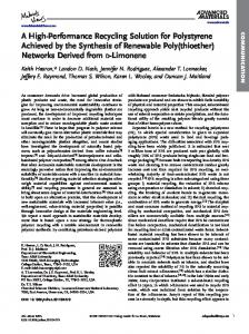
FPGA-based reconfigurable hardware provides direct execution of an algorithm. Unlike fixed-function hardware, reconfigurable logic can be reprogrammed an unlimited number of times, allowing different algorithms to execute on the same device. The FPGA is a complex system-on-a-chip that combines processors, on-chip RAM, specialized arithmetic units, and reconfigurable logic. When an algorithm kernel is mapped onto its hardware resources, an FPGA can achieve a 10-to-100 times speedup over equivalent software. Another advantage of FPGAs is that, because the device is often used to communicate to the data source, application-specific logic can be inserted into a pipelined data stream. FPGAs are already available in the marketplace for data-intensive computing tasks such as bioinformatics, text processing, and relational databases. In these experiments, we used the XtremeData XD1000 system, shown in Figure 1, which features a dual-core 2.2-GHz Opteron CPU and an Altera Stratix EP2S180F1508-C3 FPGA. Each processor has 4 Gbytes of dynamic RAM (DRAM); the FPGA additionally has 4 Mbytes of static RAM (SRAM). The Opteron and FPGA are on a dual-socket motherboard and communicate via a noncoherent HyperTransport (HT) link, with a bidirectional peak bandwidth of 1.6 GBps. The actual bandwidth achieved depends on the FPGA clock speed. Bandwidth measurements of HT communication between a test FPGA design and the Opteron showed a rate of roughly 500 MBps. Our FPGA application is written in VHDL and compiled with the Altera tool chain.
SRAM
FPGA
HyperTransport
DRAM
Opteron
DRAM
Figure 1. XtremeData XD1000 architecture. The system features a dual-core 2.2-GHz Opteron CPU and an Altera Stratix EP2S180F1508-C3 FPGA that communicate via a noncoherent HT link. Each processor has 4 Gbytes of DRAM; the FPGA additionally has 4 Mbytes of SRAM.
Scientific Imagery Analysis
The Large Synoptic Survey Telescope (www.lsst.org) will be a ground-based 8.4-meter, 102-degree-field device sited on a mountain in Chile, and is expected to start producing astronomical data in 2012. Processing LSST data will be extremely challenging. The raw data from the 3-Gpixel charge-coupled device camera is collated at a rate of 500 MBps and must be preprocessed in real time. Lawrence Livermore National Laboratory (LLNL) is a member of the LSST Corporation and contributes to the project’s camera design and data management.1
Lanczos resampling filter
Our image-processing benchmark, the Lanczos resampling filter, is derived from SWarp, 2 an application used in parts of the LSST data-processing pipeline. SWarp transforms images from the telescope to the sky template, making it possible to compare a newly acquired image with the associated sky template section and discover anomalies such as supernova explosions and gamma ray bursts. The benchmark factors out a computationally expensive and fundamental piece of the SWarp functionality for implementation: gray-scale image resampling. The input data is a gray-scale raster image (row-major order) with 8 or 16 bits per pixel. The output is a gray-scale image with 8, 16, or 32 bits per pixel. The typical SWarp execution for LSST includes resampling a 16-bit input into a 32-bit, floating-point output. It took us approximately one month to develop the Lanczos filter, including profiling SWarp to select the benchmark, designing, writing, debugging, and performance tuning.
Computational kernels
For each output pixel, SWarp applies a filter kernel that takes a weighted combination of the input pixels, specifically a Lanczos filter, to combine either 16 (4 × 4), 36 (6 × 6), or 64 (8 × 8) input pixels to generate each April 2008
33
Output bandwidth (MBps)
10,000
GPU compute GPU + PCI-E GPU + PCI-E + disk SWarp
1,000
100
10
1 1
16
36
64
1
16
36
64
1
16
36
64
1
1
1
1
4
4
4
4
16
16
16
16
Kernel sizes (upper) and Upsampling factors (lower)
Figure 2. Image resampling bandwidths. The graph shows the rate of generated output pixels in logarithmic scale as a function of upsampling scale factor and kernel size.
output pixel. The Lanczos filter kernel is convolved with the input pixels to generate the output pixels. Each input pixel has a location (x, y) relative to the projection of an output pixel into the input image. The weight used for that input pixel’s contribution to the output pixel is
π π k sin(π x) sin( x) k sin(π y) sin( y) k k , Lk (x, y) = × π 2 x2 π 2 y2 x < k, y < k where k can be 2, 3, or 4 (the so-called Lanczos2, Lanczos3, and Lanczos4 kernels), using 16, 36, or 64 input pixels per output pixel, respectively. We’ve written four resampling codes, one for each of these Lanczos convolution kernels, plus a simple nearest-neighbor filter, using NVIDIA’s Cg programming language. The Cg compiler compiles the code down to ARB Fragment Program code, an OpenGL-supported assembly code for the fragment programs on current GPUs that is vendor neutral. Because we’re benchmarking the recent NVIDIA 8800 GTX, which is a scalar GPU, it’s not necessary to optimize the computation for the more traditional four-way vectorized GPU. The philosophy behind the NVIDIA 8XXX series is to provide more scalar cores (128) rather than fewer vector cores, facilitating full utilization.
I/O methods
The SWarp implementation, which employs memorymapped I/O for large files, processes output pixels in raster order, matching the order of the data in the disk file; consequently, output is purely streaming, whereas input requires more random access. However, to better leverage the GPU’s significant processing power, mem 34
Computer
ory bandwidth, and data-caching capability, we programmed the Lanczos filter to produce the output data in 2D tiles. The benchmark generates each output pixel in the tile in a separate execution thread on the GPU. Data flows from disk to main memory, main memory to GPU memory, GPU memory back to main memory, and main memory back to disk. In each case, the program specifies the data to be moved from source to target location as a 2D rectangle. If this rectangle’s width is the same as that of the source and target, the data copy can occur as a single, contiguous stream. However, if the widths differ, the data copy must occur in a strided fashion, contiguous only at the level of
individual rows. Strided copies incur additional overhead, the largest of which are disk seeks if the striding occurs on the disk-file end of a copy between main memory and disk. Striding can also incur minor overhead when it occurs between main memory and GPU memory. Note also that, whereas support for strided copies is generally already built into GPU drivers, it’s not built into the operating system’s file I/O interface and therefore must be explicitly coded into the benchmark using some combination of reads, seeks, and buffering. The computation proceeds one output tile at a time, in row-major order. For each output tile, the program determines the input data required and loads that rectangle of data from main memory to the GPU over the PCI-E bus. The filter is then applied and the program reads the data back from the GPU to main memory over the PCI-E bus.
Performance evaluation
We used the Lanczos filter to assess the potential for accelerating LSST image-processing tasks using GPUs. Our investigation comprised numerous executions of the benchmark and the original SWarp application. Figure 2 plots performance, as measured by the rate of data output in MBps. For each execution, we chose a scale factor, which is the ratio of output pixels to input pixels, and a kernel size, which is the number of input pixels combined to generate each output pixel. GPU compute. The first column indicates the pure computational rate of our GPU-based kernel implementation. In this execution, we kept the image resident in memory and disabled data transfers to and from the GPU. In lieu of data download from the GPU, we flushed
the pipeline to allow accurate measurement of the total compute time. Predictably, this rate decreases with increasing kernel size. What might be more surprising is the dramatic increase in compute performance as the scaling factor increases. This is attributable to the highly effective 2D data (texture) cache on the GPU. As the scale factor increases, the filter repeatedly uses the same neighborhood of input pixels to generate a neighborhood of output pixels. The GPU compute column most closely relates to peak performance of the graphics hardware, analogous to peak floating-point performance from a general-purpose CPU. It exceeds 1 GBps for some kernel-size and scaling-factor combinations. GPU + PCI-E. The second column reports performance when taking into account data transfers to and from the GPU over the PCI-E bus. The time to read data back from the GPU to the host generally dominates because
tiprocessor and multicore machines, and it exhibited a nearly two-times speedup over the listed results when run on the test machine’s two processors. Conclusions. The Lanczos filter within the original SWarp implementation is purely CPU-bound; using the GPU completely eliminated the CPU bottleneck. For images that can fit into main memory such as small tiles of LSST imagery, the DRAM ↔ PCI-E communications bandwidth dominates performance. For out-of-core imagery such as large tiles or the complete sky image, the Lanczos filter is I/O-bound. The benchmark thus demonstrates that using a commodity-parallel architecture such as the GPU can provide substantial speedup over a single-CPU implementation, up to the point where disk I/O becomes the primary bottleneck. For the current test system, the I/O limited the speedup to 30 times.
Unstructured Text Processing
Language classification is an increasingly important task on the World Wide Web, where • there’s more data to read back a growing number of documents Using a commodity-parallel from the GPU than to send, due are in a language other than Engto the upsampling factor and lish. It finds uses in search-engine architecture such as the the doubling in bits (from 16 to indexing, spam-filtering heuristics, GPU can provide substantial 32) per pixel, and information retrieval, text mining, speedup over a single-CPU • raw download rates are typiand other applications that apply cally slower than upload rates. language-specific algorithms. Lanimplementation. guage classification is a key step in Performance exceeds 100 MBps for processing large document streams all combinations of kernel size and scale factor, with the and is data-intensive. best performance at 259 MBps for a kernel of one and While many solutions run on general-purpose processcale factor of 16. sors, the growth of document sets has far surpassed microGPU + PCI-E + disk. The third column reports the processor improvements afforded by Moore’s law. FPGAbenchmark’s overall performance on out-of-core data, based systems offer an alternative platform that enables using a 2D strip representation to load and store the the design of highly parallel architectures to exploit data data. The maximum output achieved is 73 MBps. For parallelism available in specific algorithms. the lowest scale factor of 1, this significantly decreases to around 40 MBps, presumably because the filter requires Language classification using n-grams significant input data as well as output data bandwidth, A well-known technique to classify a text stream’s lanand the input and output files are sharing the same two- guage is to create an n-gram profile for the language. 3 disk redundant array of independent disks (RAID). An n-gram is a sequence of characters of length exactly Experimentally disabling reading of input data from n. N-grams are extracted from a string or a document disk increased performance to around 70 MBps. by a sliding window that shifts one character at a time. SWarp. To measure real SWarp performance, shown An n-gram profile of a set of documents is the t most in the fourth column, we eliminated as many computa- frequently occurring n-grams in the set. The probability tions as possible that are extraneous to the benchmark that an input document is in a particular language is computation. In particular, we configured the resam- determined by the closeness of the document’s n-gram pling to perform in the application’s PIXEL coordinate profile to the language profile. system, thus avoiding use of any of the dozens of more In this work, we used Bloom filters4 to improve an complex astrometric coordinate transformations pos- existing FPGA-based n-gram text categorizer, the HAIL sible. The range of speedups of the GPU implementation (hardware-accelerated identification of languages) compared to SWarp ranged from 9 to 30 times. architecture, 5 to build a highly scalable design. We The need for oversampling and high-quality kernels implemented our design in VHDL on the XtremeData to produce excellent results argues that the tests with XD1000 development system. The time to select, implelarger scale factors and speedups are most applicable in ment, debug, and performance-tune the benchmark was practice. SWarp can also be executed in parallel on mul- approximately six weeks.
April 2008
35
1 Two n-grams
Host CPU
P (a)
Language classifiers
1.6 GBps HyperTransport
HT core (DMA)
8 n-grams/clock
FPGA
DDR memory Match counters
(b)
Parallel multilanguage classifier
Figure 3. Parallel Bloom-filter-based n-gram classifier hardware. (a) Multilanguage classifier. (b) Parallel multilanguage classifier on the XtremeData system.
An n-gram-based classifier builds a document’s n-gram stream by taking a sliding n-character window across the text. It generates a language’s n-gram profile by taking the top t n-grams—we selected 5,000 for our benchmark—from a representative sample of documents in that language. The classifier selects the language of an unknown document by comparing its n-gram profile to all the language profiles and selecting the language with the highest match count. Our design accomplishes n-gram tabulation using parallel Bloom filters as a probabilistic test for set membership. It streams the n-gram to k parallel hash functions, whose outputs address k separate 1 × m bit memories. To add a new n-gram, the design sets each addressed bit to 1. To test membership, the design reads all addressed bits, and finds an n-gram present in the language profile if all locations have 1 at that address. This technique can give false positives due to the hash function but won’t generate false negatives. Our parallel Bloom filter implementation uses 64 Kbits (k = 4 hash functions, m = 16-Kbit memories). The average accuracy rate for this configuration is 99.45 percent. Our design exploits parallelism at multiple levels. First, there is a separate memory for each hash function, so that all the hash functions can be applied in parallel. Second, the memories are dual-ported, so that two different n-grams can be tested in a single clock cycle, as Figure 3a shows. Finally, our design duplicates p classifiers four times, enabling eight n-grams to be processed every clock cycle, as Figure 3b shows.
Performance evaluation
We measured our implementation’s performance using the JRC-Acquis Multilingual Parallel Corpus, v3.0 (http://wt.jrc.it/lt/Acquis).6 This corpus is the body of European Union law applicable to the EU member states available in 22 European languages. We used 10 languages: Czech, Slovak, Danish, Swedish, Spanish, Portuguese, Finnish, Estonian, French, and English. For 36
Computer
our tests we parsed a subset of the corpus containing only the documents’ text bodies. There was an average of 5,700 documents for each language, with an average of 1,300 words per document. The average size of a single language corpus was 48 Mbytes, and an individual document averaged 10 Kbytes. We used 10 percent of the corpus as the training set for each language and tested the classifier on the remaining documents. To measure the system’s throughput, we used the configuration with k = 4, m = 16 Kbits accepting eight n-grams per clock, and running at a clock speed of 194 MHz. We measured the wall clock time for the transfer of documents and receipt of results in memory. The measured time didn’t include the Bloom filter programming time, which is a setup cost that can be amortized over large runs. Also, we didn’t include the preprocessing step to generate the n-gram profiles in the timing because it’s a one-time cost prior to classification. Figure 4 compares various throughput rates for our FPGA-based design as well as software only. FPGA only. The theoretical rate at which our design can accept document n-grams is 194 MHz × 8 = 1,552 million n-grams per second. Because each n-gram corresponds to a byte in the input stream, our design can perform language classification at a peak rate of 1.4 GBps. This is well within the 1.6-GBps bandwidth provided by the HT bus. However, the HT core of the XtremeData machine we used achieves only a maximum of 500 MBps and so limits the practical performance that our design realizes. FPGA + HT and FPGA + HT + I/O. By using asynchronous direct memory access (DMA) in a multithreaded communications interface to transfer data and control between the Opteron CPU and FPGA, we achieved a throughput rate of 470 MBps. When we included the time to read documents from storage in the measurements, the throughput was 93 MBps on a NAND flash drive and 55 MBps on a local Serial ATA (SATA) disk.
FLASH MEMORY I/O DRIVE
To effectively use coprocessors, the memory and I/O systems must deliver and store data at the coprocessor’s rate. Many data-intensive algorithms interact with large data sets that can’t be stored cost-effectively in main memory. While coprocessors with applicationspecific caches can accelerate in-memory computation, the bandwidth gap between volatile and persistent memory can greatly diminish the coprocessor advantage, causing I/O operations to dominate many such algorithms’ runtime. Disk storage has dramatically increased in capacity during the past decade, achieving a 60 to 100 percent compound annual growth rate between 1996 and 2004. However, latency and bandwidth have lagged, and access times for rotating media are likely to stay flat for the foreseeable future. In addition, large collections of disk drives incur costs in reliability and power usage.
Flash architectures
Strong consumer demand for music products with embedded mass storage has driven memory manufacturers to significantly lower the price and increase the capacity of flash memory chips. Flash memory is a form of nonvolatile storage in which charge trapped on a floating-gate transistor represents a data value.
10,000
FPGA only FPGA + HT FPGA + HT + I/O Software
1,000 Bandwidth (MBps)
Compared to HAIL, our equivalent FPGA + HT hardware runs 1.45 times faster on 10 languages. While HAIL can classify up to 255 languages at this rate, our hardware is limited to between 10 and 30 languages by the number of on-chip embedded RAMs. The advantage of our design is that it’s both flexible and scalable, allowing the designer to trade off the number of hash functions with memory size. Also, in contrast to HAIL, it uses only on-chip memory, eliminating the need for specific external memory configurations. Software. To compare the performance of our Bloomfilter-based classifier to that of software, we measured the system throughput of mguesser (www.mnogosearch. org/guesser), an optimized version of the n-gram-based text categorization algorithm. We ran mguesser on a 2.4-GHz AMD Opteron processor with 16 Gbytes of memory, using 10 languages for identification and 81Mbyte-size documents. Mguesser’s average throughput was 5.5 MBps, which doesn’t include the time to read the documents from disk; these were cached in memory before a timing run. In comparison, our FPGA + HT implementation is 85 times faster, and our FPGA + HT + I/O implementation is 17 times faster, than mguesser’s compute-only time. Conclusion. As with the image-resampling benchmark, this experiment showed that coprocessor technology can eliminate the CPU bottleneck of computeintensive data analysis applications at a reasonable cost in development time.
100
10
1
Implementations
Figure 4. Language classification bandwidths. The graph compares various rates of n-gram processing in logarithmic scale of our FPGA-based design as well as software.
Charge is initially deposited on each transistor in a section of the chip when an erase operation is performed, then removed when a write operation of a logical “0” occurs. Once a gate’s charge is removed, it can’t be replenished until an erase operation takes place. Given that erase operations can only be performed on large regions (128 Kbytes) of a chip at a time, a flash device can be viewed as an erasable form of write-once, readmany (WORM) storage. Memory vendors arrange floating-gate transistors in large arrays of either NOR or NAND gate structures. While NOR flash chips provide random byte access to the user, NAND flash chips feature higher capacities and better programming times. The drawback of NAND flash chips is that they operate on data in page-sized quantities (2 Kbytes). Each time a hardware controller issues a read request to a flash memory chip, the flash memory chip must locate the corresponding page in its storage array and transfer the entire page to a special buffer before the data can be moved off chip. This internal data transfer can take as long as 25 µs. Once the transfer completes, the data can be streamed out of the flash chip sequentially at a rate of 40 MBps—that is, 50 µs for a full page. To increase yields, memory vendors typically pack multiple flash dies on a single chip. For example, a 16Gbit flash chip from Micron Technologies consists of a stack of four 4-Gbit die. To increase capacity for a given printed circuit board (PCB) footprint, multiple flash chips can be stacked on top of each other using simple spacer devices. Consequently, a single socket on a PCB can house a stack of 16 or more flash memory dies. This vertical parallelism provides an opportunity to hide access time, as each die can be issued its own memory transaction, provided that no two dies simultaneously assert data on the flash pins. April 2008
37
350
Aggregate bandwidth (MBps)
300 250
ioMemory – 1 thread ioMemory – 2 threads ioMemory – 3 threads ioMemory – 4 threads RAID – 1 thread RAID – 2 threads
200 150 100 50 0 102
103
104 105 Burst size (bytes)
106
107
Figure 5. Random burst read performance of the ioMemory benchmark using multiple threads. Moving from one thread to two boosted performance by 19 to 99 percent; due to limitations of the beta version’s DMA controller, performance decreased when more than two threads were employed.
Manufacturers can likewise use horizontal parallelism to scale bandwidth by using multiple flash memory chip stacks on a PCB and striping data across the stacks. The fact that flash memory chips employ a low pin count—15 pins for the user interface—makes it possible to utilize a large number of stacks when flash-controller logic is implemented with an FPGA or application-specific integrated circuit.
ioMemory benchmark
Given the bandwidth and latency potentials of flash memory, multiple vendors are building hard-drive replacement products out of NAND flash parts. In 2007, Fusion-io, which is developing ioMemory, a PCI-E-based product, provided us with access to a beta prototype featuring 32 Gbytes of NAND flash storage built on 16 single-chip stacks of 2-Gbyte flash chips. A midsized Xilinx FPGA holds the low-level flash controller hardware and the PCI-E interface to the host. Fusion-io also provides host device drivers to make the ioMemory appear to the Linux kernel as a standard block device. We performed multiple benchmarks to observe the ioMemory’s low-level performance details. When sequentially streaming through large files, it yielded 446 MBps in read tests and 378 MBps in write tests. These speeds were roughly four times faster than a pair of SATA hard drives arranged in a software RAID 0. However, a random read test demonstrated the true potential of flash storage. In this test, multiple threads issued block read requests to random locations within a 16-Gbyte file. While the random access patterns limited the SATA hard 38
Computer
drive RAID to 30 MBps, the ioMemory achieved 328 MBps. Figure 5 presents the performance results for different burst sizes and numbers of threads. As these numbers indicate, moving from one to two threads with the ioMemory gives a sizable performance gain. This gain can be attributed to the fact that the ioMemory can process a small number of transactions concurrently, thereby overlapping access times. Performance decreased when more than two threads were employed. Fusion-io attributed this drop to limitations in the beta hardware’s DMA controller that will be fixed in the final product. Performance also dropped when bursts exceeded 128 Kbytes. This drop can be attributed to fragmentation, as the card internally stores up to 128 Kbytes of data contiguously. More recent versions of ioMemory promise even better performance, as the hardware has been scaled from 16 flash stacks to 20. This geometry scales theoretical read performance from 640 to 800 MBps.
I/O-intensive sparse graph analysis
To investigate ioMemory performance on I/O-dominated applications, we developed a graph analysis benchmark motivated by real-world applications of semantic graph analysis, which is used to discover relationships in large data sets. Graphs that represent interaction in semantic networks can become extremely large, requiring hundreds of millions of nodes. In practice, the current size limit for graph analysis is 108 nodes, while the projected need is 1012. LLNL first demonstrated breadth-first search of a 3 × 10⁹ node graph on the IBM BlueGene/L, the world’s fastest supercomputer.7 A random graph of this size is the largest that can fit in the machine’s 32,768-node memory. Subsequently, LLNL processed a 1010 -node scale-free graph using a very different approach and architecture. The breadth-first search was written as SQL queries into a relational database that stored edges in a table, and it used a 648-node Netezza server. Our benchmark graph algorithm performs out-of-core level-set expansion, a variant of breadth-first search. It runs on a standard Linux machine and uses the ext3 file system. While graph traversal can result in random reads to the file system, the out-of-core algorithm uses an optimized file-based graph layout that attempts to place adjacent vertices in the same disk block. The algorithm’s ingest phase builds the graph. It reads edges from external storage and places them in an inmemory edge buffer, from which it forms adjacency lists. It then places these lists in an in-memory adjacency buffer, and when the buffers become full, merges them into two files, a partition index file (PIF) and a partition file
160
Runtime (s)
120
D
100 80 60 40 20
(a)
0 160 140
Runtime (s)
120 100 80 60 40 20 (b)
0 160 140 120 100 80 60 40 20
(c)
ata-intensive problems challenge conventional computing architectures with demanding CPU, memory, and I/O requirements. Our experiments to date suggest that emerging hardware technologies to augment traditional microprocessor-based computing systems can deliver 2 to 17 times the performance of general-purpose computers on a wide range of dataintensive applications by increasing compute cycles and bandwidth and reducing latency. GPU and FPGA coprocessors can deliver one to two orders of magnitude increase in compute cycles through massive parallelism and application-specific caches, while high-performance I/O systems based on solid-state nonvolatile memory offer one to two orders of magnitude improvement in latency over enterprise-class harddisk drives. Our experiments demonstrate the advantages of using a coprocessor and NAND flash separately. In addition, the language classification benchmark further shows that combining the two technologies offers a substantial benefit—a 1.75 speed increase by using
Local disk ioMemory
140
Runtime (s)
(PF). The PIF holds vertices and pointers to their adjacency lists in the PF. In the search phase, the level-set expansion benchmark reads the PF and PIF to derive level set n + 1 from level set n. Our experiment used two real graphs, the Internet Movie Database (IMDB) graph (www.iruimte. nl/graph/imdb.txt) with 3.5 million vertices and the Computer Science Bibliograph (DBLP; http://dblp.unitrier.de/xml) with 1.2 million vertices and a synthetic scale-free graph with 1 million vertices and an average degree of 5. We measured runtime using six different block sizes for the graph data file (256, 512, 1,024, 2,048, 4,096, and 8,192 bytes) and two different locations for the input data sets and temporary files—a local SATA disk and ioMemory. The local disk was a Seagate Barracuda 7,200 rpm (ST380815AS), with 3 Gbps SATA volume, capable of streaming 60 MBps to Linux applications. The ingest phase, which reads in the raw graph and writes out the optimized graph layout, doesn’t benefit from the NAND flash drive. However, the read-dominated search phase showed up to a factor of two improvement in runtime when the data set and graph files were accessed from the ioMemory. Figure 6 compares the runtime of the graph benchmark’s search portion for the three graphs. Runtime is lower for all three graphs, with the DBLP graph showing the greatest benefit—an average speedup of a factor of two. Although the ioMemory bandwidth tests showed an order of magnitude improvement between disk and ioMemory random reads, the measured speedup reflects the fact that the graph algorithm can exploit vertex locality in memory and therefore doesn’t need to access the drive continuously.
0
1
2
3 4 Block size
5
6
Figure 6. Graph benchmark performance: local disk and ioMemory. (a) DBLP graph, (b) IMDB graph, (c) synthetic graph.
the ioMemory rather than local disk to stream data to the coprocessor. Speedup was limited by having to stage the data in the CPU’s memory before forwarding it to the coprocessor. Our future work will focus on methods to bypass the CPU memory and pass data directly from the flash device to the coprocessor, thereby letting the coprocessor access the data at closer to the raw NAND array rate. ■
Acknowledgments We thank John Grosh, John Johnson, John May, David Hysom, Don Dossa, Scott Kohn, Eric Greenwade, and Lisa Corsetti for their contributions to the Storage Intensive Supercomputing project at Lawrence Livermore April 2008
39
National Laboratory. This work was performed under the auspices of the US Department of Energy by LLNL under contract DE-AC52-07NA27344.
Dedication We dedicate this article to the memory of W. Marcus Miller (19 Sept. 1957-19 Feb. 2008), our coauthor and respected colleague at LLNL, without whose efforts this work wouldn’t have been possible.
References 1. R. Kolb, “The Large Synoptic Survey Telescope (LSST),” white paper, LSST Corp., 2005; www.lsst.org/Science/docs/ LSST_DETF_Whitepaper.pdf. 2. E. Bertin, “SWarp v2.17.0, User’s Guide,” Institut d’Astrophysique & Observatoire de Paris, 7 Jan. 2008; http:// terapix.iap.fr/IMG/pdf/swarp.pdf. 3. W.B. Cavnar and J.M. Trenkle, “N-Gram-Based Text Categorization,” Proc. 3rd Ann. Symp. Document Analysis and Information Retrieval, Univ. of Nevada, 1994, pp. 161-175. 4. B.H. Bloom, “Space/Time Trade-Offs in Hash Coding with Allowable Errors,” Comm. ACM, vol. 13, no. 7, 1970, pp. 422-426. 5. C.M. Kastner et al., “HAIL: A Hardware-Accelerated Algorithm for Language Identification,” Proc. 2005 Int’l Conf. Field Programmable Logic and Applications, IEEE Press, 2005, pp. 499-504. 6. R. Steinberger et al., “The JRC-Acquis: A Multilingual Aligned Parallel Corpus with 20+ Languages,” Proc. 5th Int’l Conf. Language Resources and Evaluation, ELRA, 2006; http://langtech.jrc.it/Documents/0605_LREC_JRC-Acquis_ Steinberger-et-al.pdf. 7. A. Yoo et al., “A Scalable Distributed Parallel Breadth-First Search Algorithm on BlueGene/L,” Proc. 2005 ACM/IEEE Conf. Supercomputing, IEEE CS Press, 2005, pp. 25-35.
Maya Gokhale is a computer scientist at Lawrence Livermore National Laboratory (LLNL). Her research interests include storage-intensive computing systems, reconfigurable computing, and parallel architectures. Gokhale received a PhD in computer science from the University
40
Computer
of Pennsylvania. She is a Fellow of the IEEE. Contact her at
[email protected]. Jonathan Cohen is a computer scientist at LLNL. His research interests include computer graphics and visualization, geometric algorithms, and parallel graphics architectures. Cohen received a PhD in computer science from the University of North Carolina at Chapel Hill. He is a member of the ACM. Contact him at
[email protected]. Andy Yoo is a computer scientist at LLNL. His research interests include graph mining, scalable graph algorithms, and data management systems for large-scale graphs. Yoo received a PhD in computer science and engineering from the Pennsylvania State University. He is a member of the IEEE Computer Society and the ACM. Contact him at
[email protected]. W. Marcus Miller (deceased) was a computer scientist at LLNL. He received a PhD in computer science from Colorado State University. Arpith Jacob is a PhD student in the Computer Science and Engineering Department at Washington University in St. Louis. His research interests include the design of systolic arrays and heuristic architectures for sequence analysis algorithms in computational biology. Jacob received an MS in computer science from Washington University. He is a student member of the IEEE. Contact him at
[email protected]. Craig Ulmer is a senior member of the technical staff at Sandia National Laboratories. His research interests include reconfigurable computing, novel storage technologies, and network interface processors. Ulmer received a PhD in electrical and computer engineering from the Georgia Institute of Technology. Contact him at
[email protected]. Roger Pearce is a graduate student in the Computer Science Department at Texas A&M University. His research interests include graph algorithms and robotics applications. Pearce is a student member of the IEEE Computer Society. Contact him at
[email protected].