can put wallpaper when a 2DST sheet is attached on a wall. ... We call the modified block a âmarked block .... When a single capacitance sensor is put on the.
CHI 2010: Sensing
April 10–15, 2010, Atlanta, GA, USA
High Accuracy Position and Orientation Detection in Two-Dimensional Communication Network Kei Nakatsuma Hiroyuki Shinoda Department of Information Physics and Computing, The University of Tokyo 7-3-1 Hongo Bunkyo-ku Tokyo 113-8656, Japan {tsuma, shino}@alab.t.u-tokyo.ac.jp ABSTRACT
In this paper we describe a method of high accuracy device position and orientation detection for HCI environments. Our position and orientation detection is an additional function to the Two-Dimensional Communication technology, which enables devices placed on a thin sheet to achieve two key functions for ubiquitous computing, to communicate one another and to receive electricity through the sheet wirelessly. This paper discusses the method developed to specify the positions and orientation of devices placed on the sheet. It evaluates the accuracy of obtained position and orientation through an experiment using a prototype of our positioning sensor. Author Keywords
Device localization, Two-Dimensional Communication (2DC), surface-like device, ubiquitous computing, capacitance sensing.
Figure 1. A demonstration of Two-Dimensional Communication (2DC) technology. A black sheet is the 2DST sheet. A box above the sheet is a microwave oscillator. It applies 10 watts of power into the sheet. LEDs, speakers, and fans works using the power transmitted through the sheet. Two PCs communicate with each other. The PC on the right is reading movie data from the hard drive of the PC on the left and displaying it. All devices are just touching the sheet. They can work anywhere on the sheet without any direct connection.
ACM Classification Keywords
H5.m. Information interfaces and presentation (e.g., HCI): Miscellaneous. General Terms
Experimentation. INTRODUCTION
In a building, we are almost always in contact with some surfaces like walls, floors, and desktops, etc. Therefore, many researchers have been interested in creating HCI environments on these surfaces. Especially in ubiquitous computing, several significant works have tried to develop surfaces for networking and powering infrastructures [6, 9, 15, 17]. All of them have used physical surfaces as media for data and/or power transmission. These infrastructures in the works liberate us from a constraint of batteries in conventional mobile networks. Visible and invisible human-computer interactions are enabled through these surfaces. We have proposed the Two-Dimensional Communication (2DC) technology as one solution for surface networking. It Permission to make digital or hard copies of all or part of this work for personal or classroom use is granted without fee provided that copies are not made or distributed for profit or commercial advantage and that copies bear this notice and the full citation on the first page. To copy otherwise, or republish, to post on servers or to redistribute to lists, requires prior specific permission and/or a fee. CHI 2010, April 10–15, 2010, Atlanta, Georgia, USA. Copyright 2010 ACM 978-1-60558-929-9/10/04....$10.00.
enables data and power transmission through a thin sheet named Two-Dimensional Signal Transmission sheet (2DST sheet). The technology realizes a wireless and battery-less environment as is shown in Figure 1. This paper describes a new method and prototyping for position and orientation detection of devices. We have thought that device localization on the 2DST sheet is significant in enhancing the sheet as a ubiquitous environment, and have developed the positioning function [11]. However, in our previous work, we faced a fabrication problem and could not realize a prototype. In this paper, we present prototyping of a positioning sensor using a new sensing manner. Moreover, we show its experimental results. Our final goal is to develop a surface on which devices can identify their positions and orientation as well as communicating one another and receiving electricity.
2297
CHI 2010: Sensing
April 10–15, 2010, Atlanta, GA, USA
Applications include sensor networks and input/output interfaces on surfaces in a room. Node localization in sensor networks or ubiquitous networks is one hot topic in ubiquitous computing. Our system provides sensor/ubiquitous nodes with not only location-awareness but also powering simultaneously. Input/output interfaces are also one potential application in our research. The 2DST sheet is just a medium of electromagnetic waves and cannot work like touch panels and displays. However, the sheet could have an interactive function with devices placed on the sheet. Although this way would be less interactive than conventional surfacelike devices [4, 8, 10, 14], we have advantages of scalability and cost. The 2DST sheet itself has no embedded devices or electronic components. We can enlarge the sheet easily at a low cost even across a whole room. This paper begins with an introduction of related works. Then it gives an overview of the 2DC technology. An overview and details of the proposed method follow after that. After a brief introduction of our prototype of a positioning sensor, the prototype is evaluated through an experiment. This paper ends with a description of a short summary and suggestions for future works. In the following sections, we use the term “position” as (x, y) coordinate on the 2DST sheet and the term “orientation” as rotation angle θ. Additionally we use the terms “positioning” and “localization” with the same meaning of “position and orientation detection.” RELATED WORK
Figure 2.Three layers structure of the Two-Dimensional Signal Transmission sheet (2DST sheet).
The Active badge system [18] is one of the earliest works which employs an infrared-based approach to detect the location of people in an office. The Active Bat system [19] and the Cricket system [13] use ultrasound for positioning. The RADAR system [2] is a RF-based system which uses the strength of signal from nodes with known locations. The PowerLine Positioning system [12] is a unique location system that uses signals from powerlines to detect the position in rooms. Surface-like devices are also used as interface between human and computers [4, 8, 10, 14]. In these works, locations of devices on the surfaces are also important to recognize users’ contexts and to understand their intended operations. For example, Microsoft Surface [10] detects the position of devices placed on a flat display using infrared camera behind the screen. This kind of systems also motivates our work.
Our system can be applied to a lot of fields related to HCI, especially ubiquitous computing. We introduce several projects to overview the area and to define our work’s position in the field.
TWO-DIMENSIONAL COMMUNICATION
A concept using physical surfaces as a medium for data and/or power transmission has been proposed in several works [6, 9, 15, 17]. Many of these projects try to detect the position of devices placed on the surfaces [3, 5, 6].
The 2DC is a technology to realize both data transmission and power supply on walls, floors, ceilings, desktops, and any flat surfaces in a building. Devices can connect to networks when they touch the surfaces. While sending/receiving data, they can also be supplied electricity through the surfaces simultaneously.
Networked Surfaces [15] is a device to provide high speed data transmission and electricity to devices placed on the surface. The system has also a function to detect the location and orientation of objects placed on it [5]. Pushpin Computing [9] and Pin&Play [17] provide communication and power supply environments through conductive sheets. Magic Surface [6] is also a system that shares a common goal to provide networking, power supply, and locationaware environment on a surface-like device. Not only localization systems on some surfaces, general indoor localization projects [2, 12, 13, 18, 19] are also suggestive when we consider applications of our system. Applications of these systems include ubiquitous computing, context-aware computing, sensor networks, input/output interfaces, etc.
In this section, we describe an overview of TwoDimensional Communication (2DC) technology. More details are discussed in [16].
A key device to achieve these two features of the 2DC is a thin sheet named “Two-Dimensional Signal Transmission sheet (2DST sheet).” This sheet is designed so that electromagnetic waves can propagate across it two dimensionally. Figure 2 shows a structure of the 2DST sheet. The sheet has three layers. Two conductive layers sandwich a dielectric layer. The bottom conductive layer is a continuous aluminum layer. In contrast, the upwardfacing side of the conductive layer has an aluminum meshed structure. Both conductive layers are coated by thin PET (polyethylene terephthalate) films. It is because the sheet does not connect devices placed on it directly. An internal dielectric layer is a polyethylene sheet.
2298
CHI 2010: Sensing
April 10–15, 2010, Atlanta, GA, USA
When high frequency electromagnetic waves are supplied into the sheet, they propagate across the sheet two dimensionally. While almost all energy is inside the sheet, the meshed pattern of the top conductive layer creates evanescent waves immediately above the surface of the sheet. The evanescent waves do not radiate into the air and makes it possible for devices placed on the sheet to communicate one another and to receive electricity. Since the coupling to the evanescent field requires no electrical contact, the devices can connect to networks anywhere on the sheet. This makes the technology both safer and rustproof. The 2DST sheet corresponds to the physical layer (Layer 1) of the OSI (Open System Interconnection) reference model. The sheet is just a medium of electromagnetic waves and a transformation from a conventional wireless communication environment to a 2D surface. Therefore, any wireless communication protocols including WiFi, Bluetooth, and ZigBee, etc. are available. The 2DC networks can be simply applied by replacing the existing antennas of wireless devices with a special surface connector for the sheet. Currently the 2DC technology has achieved 54 Mbps data transmission and 10 watts of power transmission through the 2DST sheet as is shown in Figure 1. PROPOSED LOCALIZATION METHOD Overview
Our location system is an “electric imaging” based technology. As is shown in Figure 2, the 2DST sheet has a meshed conductive layer. We use this layer for our location function. In the conventional 2DST sheet, the pattern of the meshed conductive layer consists of square grids. We can change the grid pattern so that it represents the position information on the sheet. It is just like that 2D barcode patterns with their position information are printed on the sheet using conductive lines. While a meshed conductive pattern is important factor to determine characteristics of data and power transmission through the 2DST sheet, we can change the pattern not to affect the propagation of electromagnetic waves inside the sheet if it is designed under the constraint that the macroscopic sheet inductance is preserved constantly [16]. A positioning sensor reads the conductive pattern when it is placed on the sheet. We employ a capacitance pattern measurement to detect the pattern. A high density capacitance sensor array can capture the conductor pattern printed on the sheet. Once the sensor detects the pattern, it acquires its own position and orientation on the sheet from the information encoded in the pattern and the relationship between a captured pattern and the sensor location. Merits of our proposed method are the followings. Firstly, our location function needs little change from the conventional 2DC technology system. The only change is a
conductive meshed pattern on the upward-facing side of the 2DST sheet. We can design the pattern not to affect the data and power transmission properties. Therefore, we can use the conventional 2DC data transmission and power supply scheme (e.g., the surface connector). Secondly, our method can work in any situation into which 2DC is able to be applied. It is because the measurement is capacitance sensing. If we use a vision-based measurement to capture the position information pattern, it cannot avoid an occlusion problem. Capacitance sensing is robust against the visible light occlusion. A piece of paper between the positioning sensor and the 2DST sheet is acceptable. We can put wallpaper when a 2DST sheet is attached on a wall. It is an advantage for aesthetic purposes and wide use of the 2DC technology in daily life. A piece of metal inhibits the location function. However we do not care about it because a piece of metal also inhibits data and power transmission. In this condition, the location function is meaningless anymore because the 2DC system does not work. The function of the proposed method is similar to the way an optical mouse detects its position. One defining difference between our 2DC positioning system and the optical mouse positioning system is that the mouse detects the relative movement of its position while the 2DC positioning determines the absolute position on the 2DST sheet. Another system which employs a similar scheme with the proposed method is Anoto’s digital pen system [1]. The Anoto’s pen detects its own position on a paper and recognizes what a user writes from an input trajectory. The pen has a small embedded camera to capture a fine dot pattern printed on a paper. The pattern is designed so that an arrangement of dots represents the position information on the sheet. The pen can acquire its absolute position on the paper. In our system, the Anoto’s embedded camera corresponds to a capacitance sensor array and the dot pattern corresponds to the conductive pattern on the 2DST sheet. Therefore, our method is just an electromagnetic way of the Anoto’s pen system. Position Information Encoding and Decoding
In order to encode the position information on the 2DST sheet, we designed the pattern of the mesh as follows. The 2DST sheet has a meshed structure as shown in Figure 2. In our position encoding scheme, one block of the grid represents one bit of information by changing its shape as is shown in Figure 3. We call the modified block a “marked block,” and the non-modified block a “plain block.” These two types of block are designed so that the difference between a plain block and a marked block does not affect the property of the electromagnetic waves’ propagation inside the 2DST sheet. Therefore, the sheet consisting of these two types of blocks can be used in a similar way to the conventional 2DST sheet. More details about the design of the shapes of the blocks appear in [11].
2299
CHI 2010: Sensing
(a) Plain block
April 10–15, 2010, Atlanta, GA, USA
(b) Marked block
Figure 3. The conductive patterns of the two types of blocks to encode one bit information in one block of the meshed grid on the 2DST sheet are shown. (a) is a plain block corresponding to low bit (0). (b) is a marked block corresponding to high bit (1). The design of a plain block is completely same as the conventional 2DST grid pattern.
Arranging marked blocks and plain blocks on the sheet forms a 2D bit pattern. We make a “Unit” which is a square region including multiple blocks. In an encoding example in Figure 4, one Unit is constructed with 5×5 blocks. A 2D bit pattern in a Unit represents its XY coordinate value and direction on the 2DST sheet. To represent direction of a Unit, there are 8 “reserved blocks” consisting of 6 marked blocks and 2 plain blocks in each Unit in Figure 4. The reserved blocks also specify one Unit’s domain. The other 17 blocks correspond to the bit pattern of the binary XY coordinate value. Practically, the bit pattern just represents an index number assigned to each Unit, and the number corresponds to the XY coordinate of the Unit. For separating neighbor Units, double width lines containing only plain blocks are used. We call this area a “Boundary zone.” It is easy to detect and identify the Boundary zone because the reserved blocks prevent any Unit from including double-width-plain-block lines inside it. When the detector is placed on the sheet, it captures the encoded bit pattern. If a whole Unit is captured completely, decoding the code is a simple problem. However, we designed the encoding scheme so that the detector can specify its own position even when it does not find a whole Unit in its captured pattern. As an example, we consider a case that the detector captures an area indicated as a red rectangle in Figure 4. In this case, the detector cannot find a whole Unit. The detector needs to determine a whole binary number assigned to a Unit under it to achieve its positioning. Following assumptions enable this. • Binary numbers encoded in Units are assigned in sequence. • We know how many Units are arranged in the horizontal and vertical direction. Here, we assume that Units are numbered from the bottom left corner of the sheet in sequence, and a number of Units in the horizontal and vertical direction on the sheet is 2N
Figure 4. The scheme to encode the position and orientation information on the 2DST sheet is shown. A basic unit is a block of the meshed grid pattern on the top layer of the sheet.
Unit size [block] Information in one Unit [bit] Sheet size (each side length) with a unique position information pattern [m] Positioning (each side length) sensor size [cm]
4 8
5 17
6 26
0.67
17.7
458.8
5.9
6.9
9.9
Table 1. The relationship between Unit size, the area of unique localization and the positioning sensor size is shown.
and 2M respectively. In this case, lower M bits of a bit sequence encoded in a Unit are invariant along a vertical direction line of Units. Similarly, upper N bits are invariant across a horizontal line of Units. If the detector can capture a bit pattern in a square area of “one Unit plus Boundary zone” (the red square area in Figure 4), captured parts of 4 neighboring Units can form one “whole” Unit. We show a practical example using a situation appeared in Figure 4. We designed as N = 9 and M = 8 in this case. A 17 bits index number assigned to the left lower Unit is n. A captured pattern by the detector includes following information. • Unit n (left lower):
0x010xxxx xxxxxxxx
• Unit n+1 (right lower):
x0xxx0xxx xxxxxxxx
N
• Unit n+2 (left upper):
xxxxxx101 0x010010
• Unit n+2N+1 (right upper):
xxxxxxxxx x0xxxxxx
2300
CHI 2010: Sensing
April 10–15, 2010, Atlanta, GA, USA
where “x” shows bits out of the captured area. We use B(n, i) for ith digit bit information (1 or 0) of the nth Unit. In this case, B(n, i) (i = 1~17) are determined as follows. • B(n, i) = B(n+2N, i) for i = 1 to 6. • B(n, 7) = B(n+2N+1, 7) and B(n, 8) = B(n+2N, 8) since B(n+2N, 1) = 0. • B(n, 9) = 0 since B(n+2N, 9) = 1 and B(n, 9) = B(n+2N, 9)+1. • B(n, 10) = B(n+2N, 10), B(n, 11) = B(n+2N, 11), B(n, 12) = B(n+1, 12), and B(n, 16) = B(n+1, 16). Finally, n is determined as n = 00010010000010010. Once the detector recognizes whole information in a Unit, it can detect its own precise position and orientation from the alignment of blocks as well as identifying the code. The accuracy of detected position depends on the spatial resolution of the detector. Sub-mesh precision is possible by a high-resolution detector. Capacitance Measurement
As is described in the previous part, the conductive pattern of position information is measured with capacitance sensing. Figure 5 shows a structure of the sensor. A square shape conductive patch is surrounded with a rectangle conductor loop. Capacitance between the patch and the loop is measured. When a single capacitance sensor is put on the 2DST sheet, some capacitors are formed between the single sensor and the conductive meshed line of the sheet if the sensor area overlaps the line. Capacitance value is in proportion to the overlapping area of the sensor with the line. Therefore, we can acquire whether the conductive line exists or not under the sensor through measuring capacitance between the patch and the loop. In addition, the pattern of the meshed conductive layer of the sheet can be detected by arranging the single sensor as an array. It makes possible to distinguish marked blocks and plain blocks presented in Figure 3. Limitation of the Proposed System
There is a tradeoff between the size of the positioning sensor and the size of the sheet on which it can localize itself uniquely. These sizes depend on the number of blocks included in one Unit. When a Unit includes 5×5 blocks as shown in Figure 4, 17 blocks are available to code an XY coordinate value. If the size of a Unit is 4×4, the number of blocks to code the position information reduces to 8. This reduces the area of the sheet with unique position information pattern. However, smaller Unit size has an advantage to reducing the size of the positioning sensor. As we described in the previous section, in order to acquire position information, at least a square area of “one Unit plus Boundary zone” is required to be captured. When the Unit size is 5×5 blocks, 7×7 blocks are required. This size is 49 mm × 49 mm when the meshed grid is 7 mm interval. The interval length 7 mm
Figure 5. The structure how the capacitance sensor works on the 2DST sheet is shown. The left upper diagram is the structure of our capacitance sensor. It measures the capacitance value between an inside conductive patch and an outside conductive loop. When the sensor is placed on the meshed line of the top layer of the sheet like the right upper image, capacitors are formed as shown in the bottom.
is equal to that of the conventional 2DC system. Considering rotation of the positioning sensor, each side is 49× √2 = 69.3 mm. Table 1 presents the relationship between the size of a Unit, a positioning sensor, and a 2DST sheet. According to Table 1, when one Unit includes 5×5 blocks, most of “handtop” size devices like cell phones, PDAs, and portable music players, etc. can determine their position and orientation uniquely on a surface which size is larger than area of typical rooms. PROTOTYPE Physical Characterization
In this section, we describe the details of our prototype system. We used the prototype to evaluate the characteristics of our localization function. A prototype of our positioning sensor is shown in Figure 6. The sensor consists of 1024 channels of discrete capacitance sensors. A size of each sensor is 2.2 mm × 2.2 mm. These discrete sensors are arranged in 2.2 mm pitch and form a 32 × 32 capacitance sensor array (the lower image of Figure 6). Here, it is required to arrange discrete sensors in an interval smaller than 2.47 mm. This is a constraint obtained from the consideration based on the sampling theorem. The whole size of its sensing area is 70.4 mm × 70.4 mm. According to Table 1, this size is large
2301
CHI 2010: Sensing
April 10–15, 2010, Atlanta, GA, USA Data Processing
A capacitance pattern image captured by the prototype sensor is shown in Figure 7 (a). We applied several simple image processing techniques to extract position and orientation information contained in Figure 7 (a). Firstly, we start from a raw data which is a matrix consisting of 32 × 32 capacitance values (Figure 7(a)). In the raw data, we see easily a lattice pattern arising from the meshed conductive line on the top layer of the sheet. We use the lattice pattern to detect the orientation angle of the sensor. Gradient of the lattice pattern corresponds to the orientation angle. The lattice pattern has enough energy so that we can find the corresponding peaked point in the 2D Fourier transform image of the raw data. The phase of the peaked point is the orientation angle normalized in 0 to 90 [deg]. After we acquire the bit pattern under the sensor, we specify an orientation of a detected Unit from a pattern of reserved blocks. We finally remove 90×N [deg] (N = 0, 1, 2, 3) uncertainty from the rotation angle. The next problem is to identify the bit pattern under the sensor. The bit pattern on the sheet is realized by arrangement of marked blocks and plain blocks. The difference between the shapes of these two types of blocks appears as the difference of the capacitance value distribution in the sensing data. We can see that discrete capacitance sensors above marked blocks tend to output higher values compared to those above plain blocks. This tendency is well consistent with the expectation from the sensor characteristics and the shapes of marked blocks and plain blocks as described previously. Therefore one easy way to distinguish a marked block from a plain block is to threshold and to binarize the raw data.
Figure 6. The positioning sensor prototype is shown. This is a 32 × 32 channel capacitance sensor array. The upper picture is the whole image of the array. The lower picture shows the bottom side of the array. Discrete capacitance sensors are arranged like this picture.
enough for unique position and orientation identification on a sheet of 17.7 m × 17.7 m. The total size of the prototype is 105 mm × 105 mm, including electrical circuits. We use Analog Devices’ capacitance sensor IC “AD7142” to acquire capacitance values from discrete sensors. In order to reduce the whole area of the sensor, we arranged measurement circuit boards vertically above the array. An “Arduino” microcontroller board controls AD7142 and acquires capacitance data. The Arduino sends detected capacitance data to PC wirelessly using Bluetooth. Once the sensor is placed on the 2DST sheet, it starts to obtain a capacitance value by request from a host PC. Once the PC receives all data from the microcontroller, it processes the data and determines the position and orientation of the device. This routine is repeated at intervals.
For the binarization, we locate each block on the data image. In other words, we specify where the meshed grid lines run in the sensing data. We have following important knowledge about the grid line in advance. • The interval between two neighbor lines is 7 mm. • The width of each line is 1 mm. We rotate the row data image by the estimated rotation angle. The rotated data is Figure 7(b). Then the rotated image is upsampled and low-pass-filtered to determine the precise mesh position as is shown in Figure 7(c). We calculate the correlation value between the upsampled pattern and the grid line template generated based on the knowledge. The correlation value becomes maximum when the template coincides with the position of the meshed grid line captured in the sensing data. Along the determined meshed grid line, we divide the upsampled image into small square domains corresponding to blocks in the meshed grid of the 2DST sheet. We generate an image whose each pixel corresponds to one block of the meshed pattern and has a value equal to the sum of all pixels’ values inside each block domain. Finally, we binarize this block resolution
2302
CHI 2010: Sensing
April 10–15, 2010, Atlanta, GA, USA
(a) Raw Data Image
(b) Rotated Data Image
(c) Upsampled the Rotating Image
(d) Obtained Bit Pattern Image
Figure 7. How data change through the data processing algorithm is shown. Starting from the raw sensing data (a), we rotate the raw data with the estimated orientation angle. The rotating data is (b). After upsampling and low-pass-filtering the rotating image (c), we obtain the bit pattern through binarization. The obtained bit pattern is (d).
image and acquire the bit pattern under the positioning sensor (Figure 7(d)).
images obtained by an infrared camera. The resolution of the ground truth system is less than 1 mm.
When the acquired bit pattern includes one whole Unit, it is easy to detect the position information encoded in the Unit. In addition, the direction of the Unit is easily obtained from the arrangement of the reserved blocks inside the Unit.
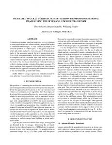
On the sheet, we acquired the position and orientation values using the prototype. Measurements were done 100 times at 100 arbitrary positions and orientations. An operator selected these points so as to disperse them on all around the sheet randomly. The selected measurement position and orientation and the positioning results are shown in Figure 8.
Accurate absolute XY coordinate values are obtained from the position information in the Unit and the relation between the whole sensing data and the location of the Unit on the data. EXPERIMENT
For an actual experimental environment, we fabricated a 2DST sheet with the position information pattern. The size of the sheet is 476 mm × 476 mm. This size is determined by implementation reasons. In Figure 10, the sheet is shown on the upper picture. In the sheet, a size of one Unit is 4×4 blocks. For an error evaluation, we obtained ground truth values using a vision-based method. We attached two infrared LEDs to the prototype. We detected their positions using
The authors found that the positioning sensor failed its measurement three times in 100 trials. In these cases, positional errors appeared over 50 mm. The failures happened when the sensing ICs misread capacitance values. As a result, an estimated position appears in a completely different point. Redundancy in a position information pattern should avoid these failures, although the required sensor size increases. Figure 9 shows the positional errors and the angular errors from the correct values. The 97 successful data eliminating three failures are plotted. All x and y errors are smaller than 4 mm and θ errors are smaller the 3 degree. In Table 2, the
2303
CHI 2010: Sensing
April 10–15, 2010, Atlanta, GA, USA
Figure 8. Ground truth and measured result points in the experiment on the sheet shown as a green rectangle. Red asterisks (*) are ground truth position of measurement points. Blue crosses (+) are measured result position. Red and blue lines show rotation angle corresponding to each point.
Positional error in experiments
mean, the maximum, and the minimum positional errors (x, y, and magnitude) and rotation angular errors (θ) are presented. Finally, Figure 10 shows the image of the experiments. The upper picture shows the positioning sensor placed on the 2DST sheet. The lower diagram is the positioning result. In the graph, we show the area of the sheet and the position and orientation of the positioning sensor. DISCUSSION
Rotation angular error in experiments
Location Accuracy
Figure 9. The positional error and the orientation angular error in the experiments are shown. The upper graph shows the positional (x and y) error from ground truth position. The lower one shows the orientation angular error to correct angular values. The 97 data eliminating three measurement failures are plotted.
In the experiment, the prototype succeeded to identify its position and orientation with positional errors less than 4 mm and rotational errors less than 3 deg. We can say that our positioning method and prototyping work well as we expected. To improve the positioning accuracy (e.g. submillimeter accuracy), higher resolution capacitance pattern sensing is required. The prototype failed its positioning three times in 100 trials. The reason is that the sensing ICs misread capacitance values. Our data processing method lacks robustness so that one channel misread could cause one bit error. Improvement of electrical circuits would stabilize the IC’s performance. Furthermore, more robust data processing algorithm and redundant bits to the position information encoding could prevent the system from determining a bit pattern incorrectly, although redundant bits contract the size of the sheet for unique position identification.
x [mm]
y [mm]
magnitude [mm]
theta [deg]
Mean
1.19
1.01
1.73
1.15
Maximum
3.70
2.76
3.70
2.71
Minimum
0.05
0.02
0.33
0.02
Table 2. The mean, the maximum, and the minimum values of positioning results’ error.
Time Requirement
One considerable problem of our system is its long measurement time. In our experiment, it took about 21 seconds to acquire one set of (x, y, θ). When our system is
applied for input/output interface devices, the real-time measurement would be desired in most cases.
2304
CHI 2010: Sensing
April 10–15, 2010, Atlanta, GA, USA
measurement. It takes 5 to several tens of milliseconds to detect a capacitance value from one channel of each discrete capacitance sensor. One possible solution to reduce the time is parallel reading from multiple sensor channels. We currently use 96 sensing ICs to acquire values from 1024 capacitance sensors. The prototype system obtains one capacitance value from one discrete sensor at a time. However, since multiple ICs can run simultaneously, we can read multiple channels in parallel. If we acquire 32 capacitance values in parallel, the measurement will consume about 1/32 less time compared to current time consumption. One demerit of the parallel reading is that it increases energy consumption. One sensing IC is driven with approximately 3 milliwatts. When Nth ICs run at the same time, energy consumption for the capacitance measurement increases to 3×N milliwatts. CONCLUSION
This paper described the method to detect the positions and orientation of devices placed on the Two-Dimensional Signal Transmission sheet. Our method is based on capacitance pattern sensing. The capacitance sensor array captures the position and orientation information encoded in the meshed conductive pattern of the top layer of the sheet. We evaluated our method and prototyping through an experiment. The result shows that the positional errors are smaller than 4 mm and the rotation angular errors are smaller than 3 deg. As a result, we succeeded the localization with millimeters precision. A wireless, batteryless, and location-aware environment was achieved. The environment can be applied for wide-range applications which enhance the interaction between us and computers. The result described in the paper is still a fundamental one. The final goal of our project is to realize actual HCI applications using our system. To achieve this, we need to improve several problems in our system. First of all, the measurement time is currently too long for real-time localization. We are planning to develop faster devices. Smaller and thinner devices are also necessary. We also plan to improve the accuracy and to verify the robustness of the measurement against various situations. Figure 10. The setup of the positioning experiment and the result are shown. The upper picture shows the positioning sensor placed on the 2DST sheet encoded with the positioning information. The middle image is the encoded 2D bit pattern. The lower diagram is the positioning result. The green square indicates the area of the 2DST sheet. The blue square shows the position and the orientation of the positioning sensor. The red point corresponds to the original point of the sensor.
ACKNOWLEDGMENTS
We would like to thank Kazuki Ochiai for supporting development of the prototype system. The research was partly supported by Grant-in-Aid for JSPS Fellows (21-5508) and National Institute of Information and Communications Technology (NICT) 13701.
Currently, the host PC takes about 1 seconds to receive all data from the sensor and to conduct the data processing. Most of remaining time is reduced by the capacitance
Finally, we would like to thank the CHI reviewers who read this paper carefully and provided useful comments.
2305
CHI 2010: Sensing
April 10–15, 2010, Atlanta, GA, USA
REFERENCES
11. Nakatsuma, K., Makino, Y. and Shinoda, H. Position sensing based on electric field measurement on TwoDimensional Signal Transmission Sheet. In Proc. of INSS 2008, 189-194.
1. Anoto. http://www.anoto.com/ 2. Bahl, P., Padmanabhan, V. N., RADAR: An in-building RF-based user location and tracking system. In Proc. of INFOCOM 2000, 775-784.
12. Patel, S.N., Truong, K.N. and Abowd, G.D. PowerLine positioning: a practical sub-room-level indoor location system for domestic use. In Proc. of UbiComp 2006, Springer (2006), 441-458.
3. Broxton, M., Lifton, J., and Paradiso, J. A. Localization on the pushpin computing sensor network using spectral graph drawing and mesh relaxation. SIGMOBILE Mobile Computing Communications Review, 10, 1 ACM Press (2006), 1-12.
13. Priyantha, N. B., Chakraborty, A., and Balakrishnan, H. The Cricket location-support system. In Proc. of MobiCom 2000. ACM Press (2000), 32-43.
4. Dietz, P. and Leigh, D. DiamondTouch: a multi-user touch technology. In Proc. of UIST 2001, ACM Press (2001), 219-226.
14. Rekimoto, J., Ullmer, B. and Oba, H. DataTiles: a modular platform for mixed physical and graphical interactions. In Proc. of CHI 2001, ACM Press (2001), 269-276.
5. Hoffmann, F. and Scott, J. Location of mobile devices using networked surfaces. In Proc. of UbiComp 2002, Springer (2002), 281-298.
15. Scott, J., Hoffmann, F., Addlesee, M., Mapp, G. and Hopper, A. Networked surfaces: a new concept in mobile networking. Mobile Networks and Applications, 7, 5, ACM Press (2002), 353-364.
6. Kishino, Y., Terada, T., Villar, N., Gellersen, H., and Nishio, S. A position detection mechanism enabling location-aware Pin&Play. In International Journal of Smart Home, 1, 1, (2007), 31-39.
16. Shinoda, H., Makino, Y., Yamahira, N. and Itai, H. Surface sensor network using inductive signal transmission layer. In Proc. of INSS 2007, 201-206.
7. Kurakake, R., Nishizawa, Y., Sakakura, K., Ouchi, H., Minami, M. and Morikawa, H. Magic surfaces: A smart building material for indoor sensing infrastructures. In Proc. of INSS 2007, 213-220. 8. Leitner, J., Brandl, P., Seifried, T., Haller, I., Yun, K., Woo, W., Sugimoto, M. and Inami, M. IncreTable, bridging the gap between real and virtual worlds. In SIGGRAPH 2008 new tech demos, ACM Press (2008). 9. Lifton, J., Seetharam, D., Broxton, M., and Paradiso, J. A. Pushpin computing system overview: a platform for distributed, embedded, ubiquitous sensor networks. In Proceedings of Pervasive 2002, (2002), 139-151.
17. Van Laerhoven, K., Villar, N., Schmidt, A., Gellersen, H.-W., Hakansson, M. and Holmquist, L.E. Pin&Play: the surface as network medium. In IEEE Communications Magazine, 41, 4, (2002), 90-95. 18. Want, R., Hopper, A., Falcão, V., and Gibbons, J. The active badge location system. ACM Trans. Inf. Syst. 10, 1, ACM Press (1992), 91-102. 19. Ward, A., Jones, A., Hopper, A. A new location technique for the active office, IEEE Personal Communications, 4, 5, (1997), 42-47.
10. Microsoft Surface. http://www.microsoft.com/surface/
2306