High-Level Design for Image Processing on FPGA Using Xilinx AccelDSP Yahia Said, Taoufik Saidani and Mohamed Atri Laboratory of Electronics and Microelectronics (EμE) Faculty of Sciences Monastir, 5000 TUNISIA E-mail:
[email protected] Abstract—This paper presents the design and implementation of image processing application on field programmable gate array (FPGA). To improve the implementation time, Xilinx AccelDSP, a software for generating hardware description language (HDL) from a high-level MATLAB description has been used. An FPGAbased architecture for Color Space Conversion has been proposed. The design was implemented on Spartan 3A DSP and Virtex 5 devices. Obtained results are discussed and compared with others architectures. Keywords-Xilinx AccelDSP; Matlab; FPGA; HLS tools; design flow; Image Processing
I.
INTRODUCTION
Image and video processing are an ever expanding and dynamic areas with applications reaching out into our everyday life such as in medicine, astronomy, ultrasonic imaging, remote sensing, space exploration, surveillance, authentication, automated industry inspection and in many more areas [1]. Reconfigurable hardware in the form of Field Programmable Gate Arrays (FPGAs) offers many performance and implementation benefits for executing video processing applications. FPGAs generally consist of logical blocks and some amount of Random Access Memory (RAM), all of which are wired by a vast array of interconnects. All logic in FPGA can be rewired, or reconfigured with different purposes as many times as a designer likes. One of the benefits of FPGA is its ability to execute operations in parallel, resulting in remarkable improvement in efficiency. The main advantage of FPGA-based design is the flexibility to exploit the inherently parallel nature of many image processing problems [2]. The difficulty of generating a design from a set of requirements and specifications increases as the system becomes complex. These difficulties led to the development of electronic system level (ESL) design and verification [3] which is an algorithm modeling methodology that focuses on a higher abstraction level using high-level languages such as C, C++, or MATLAB to model the entire behavior of the system with no initial link to its implementation. The ESL design and verification enables embedded system design, verification, and debugging for designing hardware and software implementation of custom system-on-FPGA [4].
978-1-4799-3351-8/14/$31.00 ©2014 IEEE
The Xilinx AccelDSP tool [5] is an advanced ESL design tool which transforms a MATLAB floating-point design into a hardware module that can be implemented in a Xilinx FPGA. The AccelDSP Synthesis Tool features an easy-to-use Graphical User Interface that controls an integrated environment with other design tools such as MATLAB, Xilinx ISE tools, and other industry-standard HDL simulators and logic synthesizers. This paper presents the design and implementation of FPGAbased architecture for image processing by employing Xilinx AccelDSP tool. This tool has been selected, since it can converts automatically from high-level languages (HLLs) to register transfer level (RTL) HDL and even directly to FPGA configuration bitstream [6]. The remainder of this paper is divided into five sections. After introducing, a description of the Xilinx AccelDSP design flow for implementation on FPGA is presented. Section 3 presents an example of image processing applications developed with AccelDSP which is a Color Space Conversion. Section 4 shows some discussion and remarks. Finally, concluding remarks are given in Section 5. II.
XILINX ACCELDSP DESIGN FLOW FOR IMPLEMENTATION ON FPGA
The integration of Simulink and MATLAB from The MathWorks [7] and the Xilinx FPGA design suite of tools [8], now allow embedded system development from a model-based view point which targets an FPGA. The AccelDSP software [5] is the Matlab signal processing model synthesis tool from Xilinx, which allows an algorithm developer to transform a Matlab floating-point design into a hardware module that can be implemented in silicon. Its most interesting feature is that a synthesizable RTL HDL model and a Testbench can be achieved to ensure bit-true, cycle-accurate design verification. The tool also provides scripts that invoke and control downstream tools such as HDL simulators, RTL logic synthesizers and implementation tools. Three AccelDSP implementation options (flows) are available as illustrated in “Fig.1”. The default synthesis flow is called the ISE Synthesis Flow where the main objective is to create an implementation using ISE software and verify the design using HDL gate-level simulation. The second flow is called the System Generator flow. In this flow, an IP core is
created for exporting and integrating with a larger System Generator design. The third flow, HW Co-Sim, is similar to the ISE flow but the objective is to simulate the design in hardware platform like a Virtex-4, a Virtex-5, or a Spartan-3A DSP Platform. Not only does the simulation run much faster, but this flow proves that the design will run in the target hardware. The AccelDSP IP Core Generators provide a direct path to hardware implementation for complex MATLAB built-in and toolbox functions, which when used with the AccelDSP synthesis tool, produces synthesizable and pre-verified intellectual property (IP) cores that enables and facilitate algorithmic synthesis for Xilinx FPGAs [4]. As shown in the design flow diagram in “Fig.1”, AccelDSP verifies the generated module on each step to be as true as the previous one, or to be subjectively acceptable with a small difference during the conversion from floating point design to fixed point [9]. The M-Code design normally consists of two parts: a script and function file. The script files works to create stimuli, feeds the stimuli to the function in a streaming loop and verifies the output from the function. Moreover, the script file also serves as a source file for future test bench auto generation. AccelDSP firstly analyzes the floating-point design to perform the compatibility verification of the given MATLAB code to the AccelDSP coding style guidelines. It generates architectures that work with streaming data. The streaming model to simulate the infinite stream of data entering and leaving the design is defined in MATLAB using the script-file. The second step is the verification of the Floating-Point Design. AccelDSP lets the user execute the script file inside the program and shows all plots, variables and output. The floating-point model is the golden source which must be verified by the designer using this output. Errors in this model will propagate through all later steps and exist in the final bitstream. It is also important to check that all important variables are observed since the output is used to verify the fixed-point model. Next a fixed-point design is achieved. Then the same script file is used to verify the fixed-point design, by comparing it with the saved output results of the golden model, to ensure the correctness of the design. If the results are unsatisfying, the user has to go back and annotate the design with more directives or to control or change the floating-point design. This iteration is performed until the user is satisfied with the results. The next step is to generate an RTL design and a testbench at the same time. ModelSim or other simulation tools are used to simulate the generated RTL design, which compares the testbench output with the saved fixed-point simulation output. The verification pass if all values are the same [5]. This design flow genuinely speeds up the conversion process from a Matlab model to a RTL hardware representation. What’s more, the flow can work automatically once design rules have been set [9].
Figure.1 From system specification and algorithm/model development to Xilinx AccelDSP synthesis design flow options implementations
III.
COLOR SPACE CONVERSION IP CORE DEVELOPED WITH ACCELDSP
An image processing application has been designed and developed using Xilinx AccelDSP: Color space conversion RGB to YCbCr. The proposed design was implemented on FPGA.
A color space is a mathematical representation oof a set of colors. The three most popular color models are RGB (uused in computer graphics); YIQ, YUV, or YCbCr (used in viddeo systems) and CMYK (used in color printing).However, nonne of these color spaces are directly related to the intuitive notions of hue, saturation, and brightness. All of the color spacees can be derived from the RGB information supplied by devices such as cameras and scanners [10]. Color space conversion has become an integgral part of image processing and transmission. Real time imagees and video are stored in RGB color space [11].Processing an im mage in the RGB color space, with a set of RGB values for eachh pixel is not the most efficient method. To speed up some processing steps many minance and color broadcast, video and imaging standards use lum difference video signals, such as YCrCb, makiing a mechanism for converting between formats necessary. YCbCr Color Space was developed aas part of the Recommendation ITU-R BT.601 [12] (International Telecommunication Union) for worldwide diigital component video standard and is used in television transm missions. In this color model, the luminance component is sepparated from the color components. Component (Y) represents luminance, and chrominance information is stored as two color-difference components. Color component Cb representt the difference between the blue component and a reference vaalue and the color component Cr represents the difference beetween the red component and a reference value [13].
1
Floating Point P Plot
Fixed Point Plot
3
Floating Point Model ‘Golden’
Verify Floating Point
2 project
Design directive
In-memor ry design
4
7
Verify RTL
Simulation reports
6 Verify fixed Point Generate fixed Point
analyse
Fixed Point model
5
Generate G RTL Generate system generator
RTL Mode el VHDL/Verillog
8
9 CSC:RGB to YCbCr IP Core
Figure.2 The basic steps in the AccelDSP Synthesis Flow (System Generator utput results for the CSC implementation option) with ou
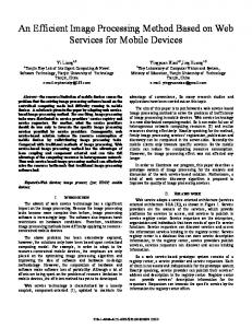
R
uint8
Input image
Serial Stream
uint8
pixel_in_R yout
In
Convert to a Serial Stream lena .jpeg
G
uint8
Input image
Serial Stream
b
Convert to a Serial Stream 1
Image From File
uint8
Input image
Serial Stream
Video Viewer
uint8
Out
Serial Stream
Output Image
Image
Video Viewer
Image
Video Viewer
Cr 0
fs_in
fs_out
val_in
val_out
Recreate Image 1
Constant 1
B
Image
Out Cb
pixel_in_B Crrout
In
Output Image
Recreate Image
y
pixel_in_G Cbout
g
Serial Stream
Out
red
In
RGB and YCbCr The basic equations to convert between R are: Y = 0.299R + 0.587G + 0.114B + 16 Cb = –0.169R – 0.331G + 0.5B + 128 Cr = 0.5R – 0.419G – 0.081B + 1228
Examine le codage style
Constant 1
CSC: RGB to YCbCr
uint8
Serial Stream
Output Image
Recreate Image 2
Convert to a Serial Stream 2 Out fs
Dis play1
Out
(1)
The above equations have been used in the inpuut M-code for the AccelDSP project to generate the hardware ccolor conversion module implemented in FPGA. Among all the color models found, YCbCr seems to be better for skin detection since the Colors in YCbCr are specified in terms of luminance (Y channel) and chrominaance (Cb and Cr channels). The main advantage of converting the image from RGB color model to the YCbCr color model iss the influence of luminance can be removed during our video processing [13].
Syste m Generator
val
Display
Figure.3 The Design Model for RGB to YC CbCr in MATLAB-Simulink/Xilinx System Geneerator
“Fig.2” shows the basic steps in the AcceelDSP Synthesis Flow (System Generator implementation optiion) with output results for the floating point and fixed point moodel respectively and the System Generator CSC IP Core generateed. The IP Core block generated is exported andd integrated with a larger System Generator design for hardwarre Co-simulation and implementation. “Fig.3” shows the desiggn that uses the generated IP Core module and Xilinx blokssets for RGB to YCbCr conversion. The hardware Co-simulatioon results for the CSC design for the input image are shown in “Fig.4”.
Figure.4 The hardware Co-simulation outputs for the CSC design
The RTL HDL Model generated is synthesized using Xilinx ISE [14] and targeted for Xilinx Spartan3A DSP and Virtex5 family. The optimization setting is for maximum clock speed. Table 1 details the resource requirements of the design. Note that in practice, additional blocks are needed for input/output interfaces, and synchronization. To provide a proper performance evaluation, the implemented CSC architecture using low cost available SpartanII development system with Xilinx chip 2S200PQ208. The properties of other designs along with ours are listed in Table 2. As seen from this table, the design of the CSC proposed by [15] requires 380 CLB on the basis clock rate of 55.159 MHz. On the other hand, our resulting architecture spent about 323CLB with a working frequency up to 83.271 MHz. Obviously, our proposed architecture has lower complexity and improved efficiency in area, thus providing a good choice in terms of lowcost hardware. IV.
DISCUSSION
From the development of FPGA technology, the methodology challenges the update of various EDA tools. Based on the standard development flow, initial efforts have been transferred to high-level design and synthesis. There are many conversion tools such as C-to-FPGA, Stateflow diagram to VHDL and Simulink/Matlab-to-FPGA. The features of Xilinx AccelDSP-to-FPGA [5] flow can be discussed as follows. •
Fast time-to-market for computer vision algorithms development. It could be described as a timely, advantageous option for developing in a much more comfortable way than that permitted by VHDL or Verilog hardware description languages (HDLs).
•
Friendly graphical user interface (GUI) that features a Design Flow Manager to guide the designer quickly through the design transformation steps. The GUI also features a Project Explorer window that lets the designer graphically browse the design hierarchy and view the M-files and the generated HDL source files.
•
AccelDSP is capable of generating a System Generator Block that can be used in a larger design. With the assistance of specified DSP blocks for FPGA, a design in Xilinx System generator can greatly shorten the development cycle from algorithm to hardware.
An important attribute of our design using AccelDSP was that the blocksets generated in AccelDSP for Xilinx System Generator, are reusable and can be neatly divided into appropriate libraries each containing blocks specific to a certain field such as (for example) Image Processing Library. The FPGA design made using high-level synthesis (HLS) tool needed much less effort than the equivalent application implementation with traditional HDLs coding. One of the beneficial features of AccelDSP is its automated and flexible floating-to-fixed-point conversion. V.
CONCLUSION
Implementation of a video processing algorithm on the FPGA is complex, tedious and error prone when using traditional design methodologies [16]. Since time-to-market is very important, it is required to look at the product development cycle to reduce the design time and gain a competitive edge in the time-to-market. Therefore, the adoption of high-level synthesis (HLS) tools is now getting into FPGA-based designing [17].
TABLE I. FPGA RESOURCES USED IN THE IMPLEMENTATION FOR THE CSC
Number of Slice Registers Number of Slice LUTs Number of LUT-FF pairs Number of bonded IOBs Maximum Frequency
Spartan 3A DSP 3400 Used Available % 255 23872 1% 464 47744 0% 128 47744 0% 75 469 16 % 53.4 MHz
Virtex 5 xc5vlx50-1ff676 Used Available % 114 28800 0% 393 28800 1% 111 396 28% 75 440 17 % 100.4 MHz
TABLE II. PERFORMANCE COMPARISON
Number of Slices Number of Slice Flip Flop Number of bonded IOBs Number of GCLKS Maximum Frequency
Used 323 453 75 1
Our Design Available 2352 4704 140 4 83.271 MHz
% 13 % 9% 53 % 25 %
Used 380 339 51 1
Design [15] Available 2352 4704 144 4 55.159 MHz
% 16 % 7% 35 % 25 %
To ease the process of transforming a MATLAB floating point design into a hardware module, Xilinx introduced the AccelDSP software for rapid prototyping of an algorithm in MATLAB into hardware. In this paper, a Xilinx AccelDSP based approach is presented for image processing applications to minimize the time to market factor. A Color space conversion (CSC) RGB to YCbCr has been designed and implemented on FPGA. The design was implemented on Spartan 3A DSP and Virtex 5 devices and their utilization summaries are compared. REFERENCES [1] [2] [3] [4] [5] [6]
J. C. Russ, “The Image Processing Hand book”, Sixth Edition, CRC Press, 2011. M. Samarawickrama, R. Rodrigo, and A. Pasqual, “HLS Approach in Designing FPGA-Based Custom Coprocessor for Image Preprocessing”, 5th international conference on ICIAF 2010,IEEE,pp. 167 -171. G. Moertti, “System-level design merits a closer look: the complexity of today's designs requires system-level”, EDN Asia, February, 01 2002, pp. 22-28. V.A. Akpan, “Model-Based FPGA Embedded-Processor Systems Design Methodologies: Modeling, Syntheses, Implementation and Validation”. Afr J. of Comp & ICTs.Vol 5, No.1 pp 1– 26, 2012. AccelDSP Synthesis Tool User Guide, Vol. UG634 (v11.4), www.Xilinx.com A. Ahmad, A. Amira, H. Rabah, Y. Berviller, “FPGA-based Architectures of Finite Radon Transform for Medical Image De-noising”, In IEEE APCCAS 2010, pp.20-23.
[7] [8] [9]
[10]
[11] [12] [13]
[14] [15]
[16]
[17]
The MathWorks Inc., MATLAB & Simulink R2009a. www.mathworks.com Xilinx Inc., www.Xilinx.com, G. Yu, T. Vladimirova, X. Wu, M. N. Sweeting, “A New High-Level Reconfigurable Lossless Image Compression System for Space Applications”, In NASA/ESA Conference on Adaptive Hardware and Systems IEEE 2008, pp. 183–190. M. Sima, S. Vassiliadis, S. Cotofana and J. T.J. Van Eijndhoven, “Color space conversion for MPEG decoding on FPGA-augmented trimedia processor”, Proceedings IEEE International Conference on ApplicationSpecific Systems, Architectures and Processors, pp. 250-259, June 2003. K. Jack, “Video Demystified: A Handbook for the Digital Engineer”, LLH Technology Publishing, Fifth Edition, 2007. ITU-R BT.601-4, 2000, “Parameter Values for the HDTV Standards for Production and International Program Exchange”, www.itu.int T. Saidani, D. Dia, W. Elhamzi, M. Atri and R. Tourki, “Hardware Cosimulation for Video Processing Using Xilinx System Generator”. Proceedings of the World Congress on Engineering 2009 Vol I, WCE 2009, July 1 - 3, 2009, London, U.K. Xilinx ISE Design Suite,www.Xilinx.com, A. M. Sapkal, M. Munot, M. A. Joshi, “R' G'B' to Y'CbCr Color Space Conversion Using FPGA”, In IET International Conference on Wireless, Mobile and Multimedia Network 2008, Volume, Issue, 11-12 Jan. 2008 pp.255 – 258. K. T. Gribbon, D. G. Bailey, and C. T. Johnston, “Using design patterns to overcome image processing constraints on FPGAs,” Third IEEE International Workshop on Electronic Design, Test and Applications DELTA, pp. 47–56, January 2006. G. Martin and G. Smith, “High-level synthesis: Past, present, and future,” IEEE Design & Test of Computers, vol. 26, no. 4, pp. 18–25, 2009.