ing a network to provide the necessary communication be- tween the tasks. ... OSI model to describe our platform. As Figure 1 ... of view. OS. For out platform the OS that manages the underlying ... NoNodes is the distance in nodes from origin to destina- tion and ... When two IPs exchange many packets it is preferably to.
Highly Scalable Network on Chip for Reconfigurable Systems ∗ T.A. Bartic, J-Y. Mignolet, V. Nollet, T. Marescaux, D. Verkest, †,‡ , S. Vernalde, R. Lauwereins ‡ IMEC, Kapeldreef 75, 3001 Leuven, Belgium †
also Professor at Vrije Universiteit Brussel, ‡ also Professor at Katholieke Universiteit Leuven {bartic,mignolet,nollet,marescaux}@imec.be
Abstract An efficient methodology for building the billiontransistors systems on chip of tomorrow is a necessity. Networks on chip promise to be the solution for the numerous technological, economical and productivity problems. We believe that different types of networks will be required for each application domains. Our approach therefore is to have a very flexible network design, highly scalable, that allows to easily accommodate the various needs. This paper presents the design of our network on chip, which is part of the platform we are developing for reconfigurable systems. The present design allows us to instantiate arbitrary network topologies, has a low latency and a high throughput.
1 Introduction Designing larger, increasingly complex systems is growing more and more difficult because of the many different issues related to the productivity and design reuse, technology and cost that have to be tackled simultaneously[1, 2]. For productivity and cost reasons, IP reuse is necessary, ideally without changing the existing designs. But building a system reusing existing IPs requires finding a way of exchanging information between them. There are different solutions to this communication problem but a disciplined and scalable one is offered by network on chips. A standard way of communication becomes even more important for dynamically reconfigurable systems. Our reconfigurable system consists of an instruction set processor (ISP) combined with reconfigurable hardware. The advantage of such a system is that it can efficiently execute a large variety of tasks with distinct requirements using a limited but reconfigurable amount of resources. Tasks can be run in their software version on the ISP or in the hardware version using the available reconfigurable hardware resources, according to the required performance and availability. Imple∗ Part of this research has been funded by the European Commission through the IST-AMDREL project (IST-2001-34379) and by Xilinx Labs, Xilinx Inc. R&D group.
menting ad-hoc, point-to-point connections between tasks implies solving a very complex and time consuming runtime routing problem. Our approach consist in implementing a network to provide the necessary communication between the tasks. The reconfigurable hardware is divided in blocks, referred as tiles, that can be reconfigured with hardware implemented tasks, referred as IPs. However, the advantage of a standard communication infrastructure is always paired with the concern for the performance loss. Applications and systems have various requirements hence networks with different capacities and services are needed. Applications with similar needs can be grouped in application domains like databases, multimedia, internet, general purpose parallel computing, etc. Considering the system that will run the applications (supercomputer, personal, mobile, . . . ), a network offering the best compromise between power, size and capacity can be designed. To address the issue of variable communication needs we have designed a highly scalable network. Together with IPs’ interfaces, the ISP and the operating system (OS) that manages all these resources, it forms a powerful yet very versatile platform. This network differs from our first design[3] by its increased scalability, and the flexibility to choose the topology and the routing algorithm. A scalable NoC was also proposed by Saastamoinen et al.[4], however their present design does not allow to build certain topologies. Our design is fully written in synthesisable VHDL and was implemented to a Xilinx Virtex2Pro FPGA. This paper continues with an overview of the whole system (Section 2), followed by the router design (Section 3), network design and characteristics (Section 4) and conclusions (Section 5).
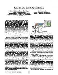
2 System overview Communication between the hardware resources will occupy a very important place in future systems on chip. From the communication point of view it is convenient to use the OSI model to describe our platform. As Figure 1 shows, at the highest level the application designer uses the services offered by the layer beneath, the
Application Presentation - Session Transport
Application Designer OS services Interfaces
The switching technique requires a finite packet size, that is given as a parameter: MaxPacketSize. Virtual cutthrough achieves, at low traffic, the same low latency as wormhole switching, paired with the same high throughput at high loads as store and forward[8]. Because in our system the size of the payload is relatively large (544 bytes, for OS efficiency reasons[9]) a wormhole switching network would saturate much faster than the virtual cut-through one. The drawback is the large buffer size required to store the packets. For this reason wormhole switching with virtual channels will be considered for a next version.
Interfaces
Network
Control & Configuration Network
Data link
Data Network
Physical
Figure 1. The structure of our platform from the communication point of view. OS. For out platform the OS that manages the underlying communication infrastructure is called operating system for reconfigurable systems (OS4RS)[5]. It is based on real time Linux on top of which specific capabilities have been added. Part of the OS is implemented in hardware[6]. The hardware part provides a standard interface to the IPs and the means to manage the data network. It also gathers statistical information over the amount of data traffic, that can be used to provide a ‘coarse’ quality of service. The transport level is implemented by the interfaces between the data network and the IPs. The control bus, carries control messages from the OS4RS to the interfaces and to the data network. The data network provides the communication between the IPs and this paper focuses on its design.
3.2 Routing Algorithm The routing algorithm is another important design choice. The taxonomy of the routing algorithms is very complex[7] but from the adaptivity point of view they can be divided in adaptive and deterministic. Our router uses a deterministic algorithm with a limited amount of adaptivity. The routing algorithm can be implemented as a finite state machine or as a look-up table, like in the current implementation. The table has an entry for each IP in the network, and its content can be changed by the OS, dynamically, at run time. Having one entry for each IP in every router offers the possibility to customize the routing for each IP at network level. The drawback is of course that the required memory space grows proportionally. This is to be compared with a finite state machine implementation that has a fixed size independent of the number of IPs but has no flexibility. This higher level form of adaptivity, could be useful in networks with a known traffic pattern. The IPs can be characterized in terms of the required data rate, and knowing the senders and the receivers for each IP, the routing tables can be modified to balance the network traffic. Each time a task that produces a change in the communication between the IPs is started, a new optimum can be computed and the tables changed accordingly. When two IPs exchange many packets it is preferably to place them next to each other. In reconfigurable systems adjacent positions can be freed by swapping IPs. The flexibility in reprogramming the routing tables can be used to avoid frequent IP relocation. Providing that there are enough free communication resources, packets can be made to travel over low traffic connections incurring minimum extra delay but saving the time required by IP swapping. The update of the routing tables takes a few clock cycles, and this type of adaptivity does not offer all the power of a hardware implemented adaptive algorithm. However, for systems with a relatively small number of IPs and a well known communication pattern, this type of flexibility will be adequate for many situations, presenting the advantage of much lower hardware requirements than would be needed for true adaptive routing algorithms.
3 Router design At the heart of the data network are the routers. Depending on topology and on the number of IPs attached to them the routers have a variable number of input and output ports. For example a router that is part of a network with a mesh topology, with bidirectional connections to 4 neighboring routers and one IP has 5 input and 5 output ports. Our router is independently parameterizable in the number of input and output ports. It allows therefore routers with unequal number of inputs and outputs. All inputs and outputs are identical no matter if they connect to another router or to an IP. All the extra functionality required by the communication with the IPs is implemented in the interfaces.
3.1 Switching technique The current implementation uses virtual cut-through switching to get a low latency: packets are forwarded as soon as they arrive if the output channel is free. The base latency (no traffic), in cycles, is given by the formula[7]: tvct = tf irst
f lit
∗ N oN odes + N oF lits
(1)
where tf irst f lit is the number of cycles required to route and switch the first flit (in our design phits are equal to flits), N oN odes is the distance in nodes from origin to destination and N oF lits is the total number of flits in the packet. 2
3.3 Router structure and implementation
our implementation on the Virtex2Pro architecture we used the available BlockRAMs. For packets of 544 bytes we can buffer up to 3 packets in one BRAM.
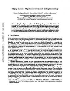
The router is built from input and output blocks connected through a shared crossbar switch (see Figure 2). Any input can be connected to any output, and there is an arbiter in every output to resolve conflicts between the different inputs. Different arbitration schemes could be used, the one that is presently implemented is acceptance dependent round robin. N Input
Routing Table S Input
Routing Table
4 Network design The network is implemented as a VHDL component, parametrized using generics. The number of the network nodes can be easily changed at design time, allowing networks of different sizes. The topology is passed as a bidimensional array, mentioning all the connections between the different routers, and between the routers and the IPs. As previously mentioned the router is independently parameterizable in the number of input and output ports (NoInPorts, NoOutPorts) allowing to build arbitrary topologies. Moreover, several IPs can be connected to one router. As shown in the introduction different networks will be required for different application domains. A flexible, easy to customize network design allows many different solutions to be simulated and synthesized in a short time, making the network optimization easier and shortening the development time.
N Output
Crossbar switch
Arbiter Output Queue S Output
Arbiter Output Queue
Figure 2. Structure of a 2 inputs, 2 outputs router. The crossbar switch can have different designs, the current one is the most straightforward using large multiplexers in a single stage. Other designs using smaller multiplexers in multiple stages would result in smaller area. The only requirement is that the crossbar switch should remain non-blocking, connections should not wait on each other, to make full use of the available resources. The data channel width (DataWidth) is parameterizable, such that the network can accommodate different capacity requirements. There is however a minimum width equal to the size of an IP address. For example a 16 nodes network, needs 4 address bits, hence the smallest DataWidth is 4. The handshaking between routers is realized through request/acknowledge lines. When a request arrives at the input block there is one clock cycle needed for the routing and then one or more cycles to get the arbiter acknowledgment, depending on the status of the output buffer. Once the request is acknowledged one flit is transmitted every clock cycle. The flow control is made at packet level, meaning that an entire packet is sent before another one can begin. As previously discussed, for virtual cut-through switching, packets have to be stored if blocked. There are several different buffering strategies. The buffers can be placed before the crossbar switch, input queueing, or after, output queueing. Our implementation uses output queueing and there is one buffer per output block. Its advantage is that it avoids head of the line blocking which occurs in input queueing. In this case, if the packet is blocked, once it is buffered the input is becomes free to receive and forward a new packet. If the next packet asks the same output then depending on the size of the output buffer the input will block or not. If the output buffer can hold more than one packet then subsequent packets can be received until the maximum number is reached (MaxNoPackets). The throughput increases with MaxNoPackets but so does the buffer size, which is equal to MaxPacketSize times MaxNoPackets. For
4.1 Area and Timing Performance The design is optimized for performance: every input block has a routing table, and every output block an arbiter and a buffer. This solution provides the shortest possible latency at the cost of silicon area. The tf irst f lit from Eq. 1 is 3 cycles. Therefore a packet traveling 5 nodes has a base latency of 15 cycles plus a number of cycles equal to the number of packet flits. For a large packet the delay to receive the first flit is only a small fraction of the time needed to receive the entire packet. Once the first flit arrives the IP can start processing the data right away, the next flits will follow every clock cycle. The overhead delay incured by the routing through the network is kept to a minimum. To save area the routing table and the arbiter could be shared by introducing a mechanism where an input or output can access them only in a certain time slot. However, for routers with a small number of ports multiplying the routing table might be a better option. For Virtex2Pro the table is very efficiently implemented using distributed dual-port selectRAMs and for one router 2 ∗ N oInP orts ∗ N oOutP orts LUTs are required. The arbiter size (see Fig. 3) grows quadratically with the number of input signals. The equivalent number of gates is given as calculated by the Xilinx tools. For a 5 inputs 5 outputs router the arbiter takes 30 slices, representing half the size of the output block and about 25% of the router’ size. For routers with more ports, like it would be needed for high dimensional network topologies, its size would increases considerably. For these topologies a centralized arbiter would result in a strong area reduction. 3
1
60 50
0.8
40
0.6
30
0.4
20
0.2
10 0
be run at 50MHz which, considering a 16 bit data channel, results in a data rate of 100MB/s per channel. 3.5
0 0
2
4 6 8 Number of input signals
10
V2Pro slices (thousands)
0.7
No. Slices Eq. Gates
0.6 0.5
1.5
0.4 1
0.3 0.2
0.5
0.1 0
0.0 4 6 8 No of Router I/Os
2.0
2
1.5
1.5
1.0
1 0.5
0.5
0.0 4 6 8 Network nodes (mesh)
10
Figure 5. Network scaling, mesh topology.
5 Conclusions Networks on chip can have different requirements in terms of latency, throughput, area and power depending on the application domain they are targeted at. A flexible network design gives the opportunity to easily search the design space for an optimum solution as well as to quickly develop the communication infrastructure of a new system. The possibility of dynamically changing the packet routing for each IP, in every router allows to better balance the network traffic, assuming that the IPs have known traffic requirements. A network using virtual cut-through switching has a low latency while maintaining a high throughput. The price to pay is the large amount of silicon area required by the buffers. For our design and bidimensional topologies the buffers took more than 97% of the total network area. However, implemented on Virtex FPGAs, depending on device and network, the available resources could be used almost in the same proportion for logic and for memory.
Equivalent Gates (millions)
0.8
2.5
2
2.5
2
The router size as a function of the number of ports (inputs = outputs) is shown in Figure 4. The equivalent number of gates represents the logic and the BRAMs used by the output buffers. The BRAMs only are responsible for more than 95% of the value. The number of slices required only by the logic shows a quadratic increase with the number of ports due to non-linear scaling of the arbiter and the crossbar switch. A better implementation of these two modules would result in improved scalability. Even so, the size of a router required for low dimensional topologies, excluding the buffers is very small.
0
Slices Eq. Gates
3
0
Figure 3. Arbiter scaling.
2
2.5
Equivalent Gates (millions)
V2Pro Slices
70
1.2
V2Pro slices (thousands)
No. Slices Eq. Gates
80
Equivalent Gates (thousands)
1.4
90
References
10
[1] A. Jantsch, H. Tenhunen, ”Networks on Chip,” Kluwer Academic Publishers, p3-18 , 2003. [2] L. Benini, G. De Micheli, IEEE Comp., p70-78, Jan 2002. [3] T. Marescaux, A. Bartic, D. Verkest, S. Vernalde, R. Lauwereins, Proc. FPL 2002, p795-805. [4] I. Saastamoinen, D. Siguenza-Tortosa, J. Nurmi, ”Networks on Chip,” Kluwer Academic Publishers, p193-213 , 2003. [5] V. Nollet, P. Coene, D. Verkest, S. Vernalde, R. Lauwereins Reconfigurable Architectures Workshop, 2003. [6] T. Marescaux, J-Y. Mignolet, A. Bartic, W. Moffat, D. Verkest, S. Vernalde, R. Lauwereins Proc. FPL 2003, (accepted). [7] J. Duato, S. Yalamanchili, L. Ni, ”Interconnect Networks, An Engineering Approach,” IEEE Comp. Soc. Press, 1998. [8] J. Rexford, K.G. Shin, Proc. Parallel Computer Routing and Communication Workshop, p116-130, 1994. [9] J-Y. Mignolet, V. Nollet, P. Coene, D.Verkest, S. Vernalde, R. Lauwereins Proc. DATE, p986-991, 2003.
Figure 4. Router scaling, for input ports equal to the output ports. Figure 5 shows the network size as a function of the number of nodes for mesh topology. Because of the fixed dimensionality of the topology (and therefore a fixed number of router ports) the size increases linearly with the number of nodes. The equivalent number of gates includes also the BRAMs used for the output buffers, which in all cases represent more than 97%. However BRAMs are very efficiently implemented in Virtex FPGAs, therefore their relative cost compared to cost of logic is strongly decreased. For a 9 nodes mesh network, implemented in a Virtex2Pro 40 the logic takes 14% of the logic resources and the buffers 17% of the available memory. The network can 4