Journal of Electron Devices, Vol. 6, 2008, pp. 182-193
© JED [ISSN: 1682 -3427 ]
Journal of Electron Devices www.jeldev.org
The Effects of Vacancy on Electronic conductance in nanowire devices Ling-Feng Mao School of Electronics & Information Engineering, Soochow University, 178 Gan-jiang East Road, Suzhou 215021, P. R. China. (Tel: 86-512-67158537; Fax: 86 512 67248370; Electronic mail:
[email protected] )
Abstract The effects of a vacancy on the electronic conductance in a finite imperfect nanowire devices represents by a sequence of delta function potential has been discussed. The results show that the position of the maximum electronic conductance in the forbidden band caused by vacancy will keep constant if the proportion between the distances from the vacancy position to the start and the end of a nanowire is the same for different number of delta function potentials. The vacancy position is found to have a large effect on the amplitude of the maximum electronic conductance in the forbidden region and results in a small shift in the position of the maximum electronic conductance, and an increase in the dimensionless strength and the number of delta function potentials will decrease the amplitude of maximum conductance in the forbidden band. Keywords: Mesoscopic systems; Nanowire device, Quantum waveguide
I. INTRODUCTION In recent years, there has been a growing interest in the electron transport in the mesoscopic conductors. Due to recent advances in nanoscale lithography and atomic layer epitaxy, nano-manufacturing has made feasible to grow nanometer-sized systems, such as arrays of quantum dots [1], molecular wires [2] and quantum wires [3]. Thus, very narrow quantum wires (the electrons are confined in a conductor with a lateral dimension on a scale of 100 nm or less) can be obtained [for example:4]. Experiments on heterostructures have led to greater interest in the case of the number of wells is finite and not very large [5-9] (The infinite periodic array is of course the famous Kronig-Penney model of a crystal). One of the most common ways to investigate the inner structure of a system is to perform scattering studies. In recent years, many authors have attempted the problem of studying the scattering of free electrons by an array of deltafunction potentials to investigate the electronic states and transport properties of one-dimensional quantum wire systems, quasiperiodic sequences, incommensurate systems [10-16]. The studies of the electronic conductance in binomially tailored quantum wires can be found in 2006 [10]. The electron transport through a series of Dirac delta-function barrier has been studied broadly [for example:11,12]. The physical characteristics of conductors with mesoscopic dimensions, such as quantum wires and dots are extremely sensitive to the presence of single defects, which may give rise to new effects. The transmission coefficient of a quantum wire in the presence of a single point defect at the wire’s cutoff frequencies has been reported by Er’el Granot [17]. The conductance of a quantum contact containing single point defects and a potential barrier has been investigated theoretically [18]. Swarnali Bandopadhyay and P. Singha Deo have shown a point defect in a single-channel quantum wire how to affect Friedel-sum-rule [19]. The transfer matrix method has been shown to be a nice way to discuss a series of Dirac delta-function barrier [12,13]. And thus, the
183 transfer matrix has been used to study the effects of vacancy on electronic conductance in the quantum wire in this work.
II. METHODS In this work, we assumed a single channel quantum wire and the scattering of electrons mainly from the geometrical structure of the potential barrier (the electron-electron interaction, and the electron-phonon interaction can be neglected). We consider a vacancy (a Dirac delta function potential has been removed from the periodic structure will result in a vacancy) existing in a finite periodic structure of Dirac delta function potential. Using Schrödinger theory, the eigen values equation for energie can be written as
h2 d ⎡ 1 d ⎤ − ψ + U (x )ψ = Eψ 2 dx ⎢⎣ m dx ⎥⎦
(1)
where m is the dependent effective mass of the position and U(x) is the periodic potential energy h is the reduced Planck’s constant, E is the electron energy. Firstly we considered the solution of Schrödinger equation for a single Dirac delta potential with the strength φ ( U ( x ) = φδ ( x − x 0 ) ) located at the position of x 0 . The solution for the region where the potential is zero can be written as
⎧ A0 e ikx + B0 e − ikx ikx − ikx ⎩ A1e + B1e
x < x0 x > x0
ψ (x ) = ⎨
(2)
The boundary conditions has been considered in the following. It is clear that when x → x0 , the integral on the right of Eq.1 goes to zero, so we can obtained:
h 2 ∂ 2ψ = φδ ( x − x0 )ψ 2m ∂x 2
(3)
Integrating both side the equation from x0 − Δ → x0 + Δ ,
∂ψ ∂x
− x0 + Δ
∂ψ ∂x
= x0 − Δ
2mφ ψ (x0 ) h2
(4)
The other boundary condition can be written as
ψ
x0 + Δ
=ψ
(5)
x0 − Δ
Based on the boundary conditions, solving the Schrödinger equation the following equation can be obtained:
mφ ⎛ ⎛ A0 ⎞ ⎜ 1 + i kh 2 ⎜⎜ ⎟⎟ = ⎜ ⎝ B0 ⎠ ⎜⎜ − i mφ e 2ikx0 ⎝ kh 2
mφ − 2ikx0 ⎞ e ⎟⎛ A ⎞ kh 2 ⎟⎜ 1 ⎟ mφ ⎟⎜⎝ B1 ⎟⎠ 1− i 2 ⎟ kh ⎠ 2mE where k is the wave number given by . h2 i
(6)
For a series of periodic Dirac delta potential barrier, the following relation can be obtained: n ⎛ A0 ⎞ ⎛A ⎞ ⎛A ⎞ ⎜⎜ ⎟⎟ = M t ⎜⎜ n ⎟⎟ = ∏ M j ⎜⎜ n ⎟⎟ ⎝ B0 ⎠ ⎝ Bn ⎠ j =1 ⎝ Bn ⎠
(7)
where:
mφ ⎛ ⎜ 1+ i 2 kh Mj =⎜ ⎜ − i mφ e 2ikx j ⎜ ⎝ kh 2
i
mφ − 2ikx j ⎞ e ⎟ kh 2 ⎟ mφ ⎟ 1− i 2 ⎟ kh ⎠
(8)
Let Bn=0, and A0=1, the transmission amplitude An through a series of periodic Dirac delta potential barrier can be obtained as
An =
1 M t (1,1)
(9)
184 The solution to a series of periodic Dirac delta potential barrier using transfer matrix method can be found in Ref.[for example:9,12,13,20] The M t (1,1) is the first element in the first row in a 2×2 matrix. According to the Landauer-Buttiker formula [21], the electronic conductance G (the first derivative of the current-voltage characteristic, G=dI/dV) through this structure is:
G=
2e 2 An h
2
(10)
where h is the Planck’s constant.
III. RESULTS AND DISCUSSION In the calculations of electronic conductance through a nano-wire, a dimensionless strength
Ω=
mdφ π 2h 2
(where d is
the distance between the adjacent barriers) for Dirac delta function potential was used in this work according to references [10,22]. In the following part, the effects of a vacancy on electronic conductance through a quantum wire have been studied in detail. And in all calculation for the imperfect case, only one vacancy exists in the quantum wire. In Fig.1, the electronic conductance spectrums in unit
2e 2 h
of perfect and imperfect finite periodic Dirac delta function
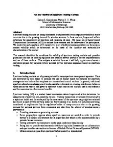
potential have been plotted (the number of Dirac delta function is 55 and the dimensionless strength is Ω = 0.2 ). For the imperfect case in this work, it means a vacancy existing in such a periodic potential system, which is formed by removing one potential barrier from the periodic structure. The electronic conductance spectrums in Fig.1 show the conduction band due to coherent tunneling of electronic waves and the forbidden band due to destructive interference of electronic waves. A vacancy existing in the quantum wire will deteriorate the electronic conductance in the conduction band region due to destructive interference of electronic waves. This behavior can be clearly seen from Fig.1. From this figure, the most affected conduction band by a vacancy is observed to be the lowest conduction band. And thus, in the following discuss, detailed studies will be done around only the lowest conduction band. Firstly, the change in electronic conductance in the forbidden band caused by vacancy will be discussed in detail. Fig. 2a, b shows the detailed electronic conductance spectrums in unit
2e 2 h
of perfect and imperfect quantum wires near the
lowest conduction band respectively. The number of Dirac delta function potentials changed from 10 to 55, and the dimensionless strength is Ω = 0.2 . It is noted that in the calculations for Fig.2b, Fig.3, Fig.5b and Fig.6 the vacancy position has been always chosen at where it is located at the 0.63 time of the length of quantum wire. Comparing Fig.2b to Fig.2a, it is clearly seen that an abrupt change in electronic conductance (it also means a transmission resonance) in the forbidden band cause by the vacancy. All these results show that a vacancy in a quantum wire has both effects: one is that it can deteriorate the electronic conductance in the conductance band; the other is that it can result in a large electronic conductance in the forbidden band. The characteristic of such a large electronic conductance in the forbidden band will be given in detail in the following part. The position of the maximum electronic conductance and its amplitude are two important properties of such a maximum electronic conductance. Fig.3 shows that the position of the maximum electronic conductance will not change when the number of Dirac delta function potentials changes (because only one vacancy exist in the quantum wire, different vacancy concentration is equivalent to different number of Dirac delta function potentials). It is noted that there has been another condition in the calculations, which is that the position of the vacancy is always located at the 0.63 time of the length of quantum wire for all imperfect quantum wires. It implies that if the ratio of the distance from the position of the vacancy to the start of the quantum wire to that of the end keep constant, the position of the maximum electronic conductance will keep constant with the number of Dirac delta function potentials changing. The amplitude of electronic conductance in the forbidden region caused by the vacancy can be clearly observed to obey a parabola relation in Fig.3. It can be easily understood because the destructive interference of electronic waves caused by the vacancy will decrease when the number of Dirac delta function potential increases.
Secondly, the effects of the change in vacancy position on the position of the maximum electronic conductance and its amplitude will be discussed in the following. Fig.4a gives the detail characteristic of the maximum electronic conductance and its amplitude caused by the vacancy in the forbidden band while the 3rd and the 5th Dirac delta function potential has been removed respectively (the number of Dirac delta function is 10 and the dimensionless strength is Ω = 0.2 ). Fig.4b gives the detail characteristic of the maximum electronic conductance and its amplitude caused by the vacancy in the forbidden band while the 3rd and the 51st Dirac delta function potential has been removed respectively (the number of Dirac delta function is 55 and the dimensionless strength is Ω = 0.2 ). It can be clear seen in Fig.4a,b that the vacancy position will have a large effect on the amplitude of the maximum electronic conductance and a small shift in its position. At last, the relation between the effects of a vacancy on electronic conductance through quantum wire and the dimensionless strength will be discussed. Fig. 5a, b shows the electronic conductance spectrums in unit
185
2e 2 of perfect and imperfect quantum wires near the lowest conduction band respectively for different h dimensionless strength (the number of Dirac delta function potentials is 20). Comparing Fig.5b to Fig.5a, it is clearly seen that an abrupt change of the electronic conductance in the forbidden band how to change with the dimensionless strength Ω . The detailed properties of such a large electronic conductance in the forbidden band will be given in Fig.6. The position of the maximum electronic conductance will shift to higher energy when the dimensional strength increasing (the increase in the strength of potential and the distance between the adjacent barriers can result in an increase in dimensional strength) can be seen in Fig.5 and Fig.6. Further, the amplitude of maximum electronic conductance caused by the vacancy in the forbidden band decreases nearly exponential with the dimensionless strength and a parabola relation between its position shift and the dimensionless strength can be observed in Fig.6. All these can be understood that the destructive interference of electronic waves caused by the vacancy will decrease when the dimensionless strength increases.
IV. CONCLUSION For one vacancy existing in a nanowire device, the electronic conductance in the conduction band will be deteriorated due to destructive interference of electronic waves. The position of the maximum electronic conductance in the forbidden band will not change if the ratio of the distance from the position of the vacancy to the start and to the end of nanowire keeps constant. A parabola dependence of the amplitude of the maximum electronic conductance in the forbidden band caused by a vacancy on the number of Dirac delta function potential is found. The vacancy position is found to have a large effect on the amplitude of electronic conductance and a small shift in its position. The amplitude of electronic conductance in the forbidden band caused by the vacancy is found to decrease nearly exponential with the dimensionless strength. The position of the maximum electronic conductance will shift to higher energy when the dimensional strength increases. Acknowledgements: The author acknowledges financial support from the National Natural Science Foundation of China (NSFC) grant No. 60606016.
References [1] A.W. Holleitner, C.R. Decker, H. Qin, K. Eberl, R.H.Blick, “Coherent Coupling of Two Quantum Dots Embedded in an Aharonov-Bohm Interferometer”, Phys. Rev. Lett. 87, 256802, (2001). [2] A.I. Yanson, G. Rubio-Bollinger, H.E. van den Brom, N. Agraít, J.M. van Ruitenbeek, “Formation and manipulation of a metallic wire of single gold atoms”, Nature (London) 395, 783 (1998). [3] A.T. Tilke, F.C. Simmel, H. Lorenz, R.H. Blick, J.P. Kotthaus, “Quantum interference in a one-dimensional silicon nanowire”, Phys. Rev. B 68, 075311 (2003). [4] Shin-ichi Osako, Tsuyoshi Sugihara, Yoshitaka Yamamoto, Toshihiko Maemoto, Shigehiko Sasa, Masataka Inoue, and Chihiro Hamaguchi, “Quantum anti-dot arrays and quantum wire transistors fabricated on InAs/Al0.5Ga0.5Sb heterostructures”, Semicond. Sci. Technol. 11, 571 (1996). [5] S. E. Ulloa, E. Castan˜o, and G. Kirczenow, “Ballistic transport in a novel one-dimensional superlattice”, Phys. Rev. B 41, 12350 (1990). [6] Hua Wu, D. W. L. Sprung, J. Martorell, and S. Klarsfeld, “Quantum wire with periodic serial structure”, Phys. Rev. B 44, 6351 (1991). [7] T. M. Kalotas and A. R. Lee, “One-dimensional quantum interference”, Eur. J. Phys. 12, 275 (1991). [8] T. M. Kalotas and A. R. Lee, “Spectra of periodic potentials in finite boxes”, Eur. J. Phys. 16, 119 (1995). [9] D. J. Griffiths, and N. F. Taussig, “Scattering from a locally periodic potential”, Am. J. Phys. 60, 883 (1992). [10] H.S.Ashour, A.I Ass'ad, M.M. Shabat, and M.S.Hamada, “Electronic conductance in binomially tailored quantum wire”, Microelectronics J. 37, 79 (2006) [11] G.J. Jin, Z.D. Wang, A. Hu, S. S. Jiang, “Quantum waveguide theory of serial stub structures”, J. Appl. Phys. 85, 1597 (1999). [12] D. W. L. Sprung, J. D. Sigetich, Hua Wu, and J. Martorell, “Bound states of a finite periodic potential”, Am. J. Phys. 68, 715 (2000) [13] D.W.L. Sprung, Hua Wu, J. Martorell, “Scattering by a finite periodic potential”, Am. J. Phys. 61, 1118 (1993) [14] P.K. Thakur, C. Basu, “Characterisation of the delocalised states in a continuous correlated disorder model”, Physica A 217, 289 (1995). [15] P.K. Thakur, C. Basu, “Existence of cross-over states in electronic transmission due to delta-function potential with inhomogeneous and slowly varying periods”, Physica A 216, 45 (1995). [16] R. Farchioni, G. Grosso, “Localization properties of Krönig-Penney incommensurate potentials”, Phys. Rev. B 51, 17348 (1995).
186 [17] Er'el Granot, “Transmission coefficient for a point scatterer at specific energies is affected by the presence of the scatterer but independent of the scatterer's characteristics”, Phys. Rev. B 71, 035407 (2005) [18] Ye. S. Avotina, and Yu. A. Kolesnichenko, “Nonlinear conductance of a quantum contact containing single impurities”, Low Temp. Phys. 30, 153 (2004) [19] Swarnali Bandopadhyay, and P. Singha Deo, “Friedel sum rule for a single-channel quantum wire”, Phys. Rev. B 68, 113301 (2003). [20] P. Exner, M. Tater, and D. Vanĕk, “A single-mode quantum transport in serial-structure geometric scatterers”, J. Math. Phys. 42, 4050 (2001). [21] Y. Takagaki, D.K. Ferry, “Electronic conductance of a two-dimensional electron gas in the presence of periodic potentials”, Phys. Rev. B 45, 8506 (1992). [22] S. J. Blundel, “The Dirac comb and the Kronig-Penney model: Comment on ``Scattering from a locally periodic potential,'' by D. J. Griffiths and N. F. Taussig [Am. J. Phys. 60, 883–888 (1992)]”, Am. J. Phys. 61, 1147 (1993).
187 Captions
2e 2 of perfect and imperfect quantum (one vacancy) Fig. 1. Electronic conductance spectrums in unit h wires (the number of Dirac delta function is 55 and the dimensionless strength is Ω = 0.2 ) 2e 2 of perfect (a) and imperfect (one vacancy) (b) Fig. 2. Electronic conductance spectrums in unit h quantum wires (the number of Dirac delta function changes from 10 to 55, and the dimensionless strength is Ω = 0.2 ) Fig. 3. The position of the maximum electronic conductance and its amplitude in the forbidden band caused by a vacancy for different vacancy concentration (the number of Dirac delta function changes from 10 to 55, only one vacancy exists in the quantum wire, and the dimensionless strength is Ω = 0.2 ) Fig. 4. The position of the maximum electronic conductance and its amplitude in the forbidden band caused by a vacancy for different vacancy position (the number of Dirac delta function is 10 (a) and 55(b) with the dimensionless strength is Ω = 0.2 ).
2e 2 of perfect (a) and imperfect (one vacancy) (b) h quantum wires (the number of Dirac delta function is 20 and different dimensionless strength Ω ). Fig. 5. Electronic conductance spectrums in unit
Fig. 6. The position of the maximum electronic conductance and its amplitude in the forbidden band caused by a vacancy for different dimensionless strength Ω and the number of Dirac delta function barrier is 20 (only one vacancy exists in the quantum wires).
188
no vacancy
1.0
one vacancy
0.8
G
0.6 0.4 0.2 0.0 0
1
2
3
4
kd/π
Fig.1
5
6
1 1E-5 1E-10 1E-15 1E-20 1E-25 1E-30 1E-35 1E-40 1E-45 1E-50 1E-55 0.0
The number of dirac potental: 10 15 20 25 30 35 40 45 50 55 0.2
0.4
0.6
0.8
1.0
1.2
kd/π (a)
G
G
189
1 1E-5 1E-10 1E-15 1E-20 1E-25 1E-30 1E-35 1E-40 1E-45 1E-50 1E-55 0.0
vacancy concentration: 10.0% 6.7% 5.0% 4.0% 3.3% 2.8% 2.5% 2.2% 2.0% 1.8% 0.2
0.4
0.6
kd/π (b) Fig.2
0.8
1.0
1.2
1.4
1
1.2
1E-5
1.0
1E-10
0.8
1E-15
kd/π
0.6
1E-20
0.4
1E-25
0.2 0.0
1E-30
-0.2
1E-35
-0.4
1E-40
-0.6 2
3
4
5
6
7
8
Vacancy concentration (%)
Fig.3
9
10
1E-45
The amplitude of G
190
191
0.1
Vacancy occurs at the 3rd barrier the 5th barrier
G
1E-3
1E-5
1E-7 0.398
0.400
0.402
0.404
0.406
kd/π (a)
1E-47 1E-48
Vacancy occurs at the 3rd barrier the 51th barrier
G
1E-49 1E-50 1E-51 1E-52 1E-53 0.398
0.400
0.402
kd/π (b) Fig.4
0.404
0.406
G
192
1 1E-5 1E-10 1E-15 1E-20 1E-25 1E-30 1E-35 1E-40 1E-45 1E-50 1E-55 0.0
Ω:
0.1 0.3 0.5 0.7 0.9 0.2
0.4
0.6
0.8
0.2 0.4 0.6 0.8 1.0 1.0
1.2
kd/π
G
(a)
1 1E-5 1E-10 1E-15 1E-20 1E-25 1E-30 1E-35 1E-40 1E-45 1E-50 1E-55 0.0
Ω:
0.1 0.3 0.5 0.7 0.9 0.2
0.4
0.6
kd/π (b) Fig.5
0.8
0.2 0.4 0.6 0.8 1.0 1.0
1.2
193
0.50
1E-5
kd/π
0.45
1E-10 1E-15
0.40 1E-20 1E-25
0.35 0.0
0.2
0.4
0.6
0.8
1.0
The dimensionless strength Ω
Fig.6
1E-30
The amplitude of G
1