Implementation of a Probabilistic Neural Network for Multi-spectral Image Classification on an FPGA Based Custom Computing Machine Marco A. Figueiredo
[email protected] SGT, Inc. / NASA Goddard Space Flight Center Greenbelt, Maryland , USA Clay Gloster
[email protected] Department of Electrical & Computer Engineering North Carolina State University, Raleigh, NC, USA Abstract As the demand for higher performance computers for the processing of remote sensing science algorithms increases, the need to investigate new computing paradigms is justified. Field Programmable Gate Arrays enable the implementation of algorithms at the hardware gate level, leading to orders of magnitude performance increase over microprocessor based systems. The automatic classification of space borne multispectral images is an example of a computation intensive application that only tends to increase as instruments start to explore hyperspectral capabilities. A probabilistic neural network is used here to classify pixels of a multispectral LANDSAT-2 image. The implementation described utilizes a commercial-off-the-shelf FPGA based custom computing machine.
1. Introdution A new generation of satellites is under implementation by the National Aeronautics and Space Administration (NASA) to compose the Earth Observing System (EOS). The instruments aboard the EOS satellites not only extend the observation life of the current system, but they also expand the capabilities of remote sensing scientists to better understand the Earth’s environment. Along with the scientific advancements of the new missions, it is also necessary to explore new technologies that facilitate and reduce the cost of the data analysis process. In order to process the high volume of data generated by the new EOS satellites, NASA is constructing the Distributed Active Archive Centers (DAACs), an expensive and powerful parallel computing environment. Scientists will be able to request certain data products from these centers
for further analysis in their own computing systems. A new technology that could bring the processing power to the scientist’s desk is highly desirable. The ultimate scenario would be for the scientist to request the data directly from the satellite along with historic data from an archive center. The advent of Field Programmable Gate Array (FPGA) enables a new computing paradigm that may represent the future for remote sensing scientific data processing. Several applications utilizing FPGA based computers have been developed showing orders of magnitude acceleration over microprocessor based systems [3],[4],[5]. Moreover, microprocessors and FPGAs share the same underlying technology – the silicon fabrication process. Therefore, it is reasonable to conclude that FPGA based machines will always outperform microprocessor based systems by orders of magnitude [6],[7]. The Adaptive Scientific Data Processing (ASDP) group at NASA’s Goddard Space Flight Center (GSFC) has been investigating the utilization of FPGA based computing, also kown as adaptive or reconfigurable computing, in the processing of remote sensing scientific algorithms. The first prototype developed by the group utilized a comercial-off-the-shelf (COTS) reconfigurable accelerator in the implementation of an automatic classifier for the LANDSAT-2 multispectral images. The classifier algorithm utilizes a probabilistic neural network (PNN). The results show an order of magnitude performance increase over a high-end workstation. This paper presents details of the FPGA design and is organized as follows. Section 2 describes the PNN algorithm. The implementation of the FPGA custom computing machine is then presented. Finally, a performance analysis is given.
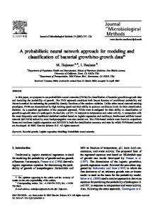
2 The PNN multispectral image classifier Remote sensing satellites utilize multispectral scanners to collect information about the Earth’s environment [8]. The images formed by such instruments may be seen as a set of images each corresponding to one spectral band. A multispectral image’s pixel is represented by a vector of size equal to the number of bands. The combination of the multiple spectrum measurements represented by each element of the pixel vector determine a signature that correspond to a physical element. Through the observation of an image and the comparison of certain pixels to elements from known locations (in-situ measurements), a scientist is able to identify signatures and compose classes. These classes contain representations of multispectral pixels that are closely related. Several neural network schemes have been devised for the automatic classification of multispectral images [1]. One in particular, the Probabilistic Neural Network (PNN) classifier presented good accuracy, very small training time, robustness to weight changes, and negligible retraining time. A description of the derivation of the probabilistic neural network (PNN) classifier is given in Chettri et al., 1993 [2]. The same algorithm and data set used in [2] were used in this work to demonstrate the effectiveness of FPGA based computing. The Blackhills (South Dakota, USA) data set was generated by the Landsat 2 multispectral scanner (MSS). The image’s 4 spectral bands (0.5-0.6 um, 0.6-0.7 um, 0.7-0.8 um, and 0.8-1.1 um) correspond to channels 4 through 7 of the Landsat MSS sensor. There are 262,144 pixels corresponding to a 512x512 image size, and each pixel represents 76m x 76m on the ground; the images were obtained in 1973. The ground truth was provided by the United States Geological Survey. Table 1, extracted from [2], shows the distribution of the image data.
0 1 2 3 6
Training Number of Pixels 453 478 464 482 368
Entire Image Number of Pixels 6676 42432 16727 198868 1441
Class name USGS – Level 1 Urban Agricultural Rangeland Forested Land Barren
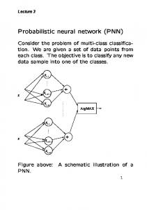
Table 1 - Distribution of data, Blackhills data set Figure 1 illustrates the PNN classifier procedure. Each multispectral pixel, represented by a vector, is compared to a set of pixels belonging to a class. Equation 1 is used to derive a value that indicates the probability that the
pixel fits in that class. A probability value is calculated for each class. The highest value indicates the class in which the pixel fits in.
Figure 1 - PNN Image Classifier
Equation 1- PNN classifier
3 The FPGA implementation Field Programmable Gate Arrays (FPGA) are logic devices that offer in-circuit re-programmability. Adaptive, or reconfigurable, computing is an emerging technology that utilizes FPGAs to implement computation intensive algorithms at the hardware gate level. As a result, acceleration rates of several orders of magnitude faster than current computers are attainable. A set of FPGA devices arranged in some kind of programmable interconnection network is called a reconfigurable or adaptive computer. Current reconfigurable computers function like coprocessor cards which are plugged into desktop or large computer systems, called the host. By attaching a reconfigurable coprocessor to a host computer, the computation intensive tasks can be migrated to the coprocessor forming a more powerful system. The first task in the implementation of an application is to select the adaptive coprocessor that best matches the
algorithm in question. At the current state of the technology, there is no single COTS coprocessor card that will give best performance in most applications. A preliminary analysis of the PNN classifier indicated that the Giga Operations Spectrum System [9] presented the best architecture for its modularity and expandability.
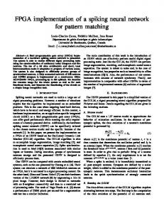
3.2 FPGA application design Figure 4 shows the architecture of the X213 module. The YFPGA has a direct connection to the host through the HBUS. The memories between the two FPGAs were not used. An interconnection bus was used to transfer data from the X to the YFPGA instead. The HBUS was also extended from the Y to the XFPGA to allow the host to read back the results of the YFPGA. Only the SRAM banks on the XMEMBUS and HMEMBUS were utilized.
Figure 2 - G900 Spectrum System The Giga Operations Spectrum System, shown in figure 2, is composed of a PCI bus based motherboard and 16 plug-in modules, 4 stacks of 4 modules each. These plug-in modules contain two Xilinx FPGA devices and provide the gate capacity based on the type of FPGA device being used. Our design was developed based on Xilinx XC4013E FPGA devices with an equivalent 13,000 gates per each device, or 26,000 gates per X-213 module.
3.1 Algorithm partitioning
Figure 3 - Algorithm Partitioning The computation intensive portion of the multispectral image classification algorithm resides on the calculations within the PNN classifier. The user interface, data storage and IO, and adaptive coprocessor initialization and operation is performed on the host computer. The PNN classifier was mapped to a single X213 module. Figure 3 illustrates the algorithm partitioning.
Figure 4 - X213 Block Diagram Due to limited number of gates available on a single FPGA, it was not feasible to use floating point arithmetic in our implementation of the PNN algorithm. Hence we transformed the algorithm into fixed point prior to hardware implementation. The width of the fixed point data path was determined by simulating variable bit operations in C and comparing the results obtained from the original algorithm in floating point. Once the fixed point classification of the Blackhills data set yielded the same results as the floating point version, data path width for the FPGA implementation was no longer varied. Figure 5 shows the data flow diagram for the hardware implementation of the PNN classifier. The number of bands (d) was fixed to 4, the maximum value of the number of weights per class (Pk) was fixed to 512, and the maximum number of classes (k) was set to 16. As shown in equation 1, there are two constants, K1 and K2, that are class dependent. These constants are precalculated on the host and downloaded to memory banks residing on the FPGAs. The weights memory was mapped to the HMEM SRAM. Due to the lack of space on the XFPGA, the K1 multiplier and the class comparison blocks were moved to the host. These calculations amount to k (number of classes) multiplications and comparisons per pixel classification. Overall, they do not account for a significant amount of the computation, leading to a small performance penalty. A 4-bit register holds the number of classes. This register is initialized by the host before loading the FPGAs. The weight memory can be as large as 16*512*4*2bytes = 32768 16-bit words. The weight
Figure 5 - PNN Data Flow Diagram values are 10-bits wide. Since each class can have up to 512 weights, an array that holds the number of weights for each class is used. The arrays’ data inputs are connected to the HBUS allowing visibility from the host application. The Subtraction Unit subtracts W, a 4 x 10-bit element vector for W (w0, w1, w2, w3) and X (x0, x1, x2, x3). The result of the subtraction ranges from -1023 to 1023, requiring 11 bits to be represented in two’s complement format. The Square Unit multiplies the 11-bit elements of the Y vector by themselves (t0 = y0 * y0). The values of the elements of vector T range from 0 to 1,046,529, asking for 20 bits to be represented in two’s complement format. The Band Accumulator Unit adds the 4 elements of the T vector delivering u, which value ranges from 0 to 4,186,116, requiring 22 bits. The K2[K] Memory holds the K2 values for each class. K2 = ½ σΚ−2 , where σΚ varies between 2 and 12, with increments of 1. As a result, K2 varies between 0.125 (σ = 2), and 0.003472 (σ = 12). The largest value of K2 = 0.125 is represented in binary by 0.001. In order to increase the precision of the multiplication, the values of K2 are stored with the decimal point shifted to the right by 2 (a multiply by four effect). After K2 is multiplied by u in the Multiplier 1 Unit, the decimal point of the result of the multiplication is shifted to the left by 2 (divide by 4 effect). Since this is a representation issue, no hardware is
necessary to perform the shifts in the YFPGA, only the host needs to stores the values in the K2[K] memory in the above mentioned format. The K2 Multiplier Unit multiplies the K2 values for each class by the accumulated values of the difference between a pixel and a weight vector. It delivers a 44-bit result to the TO_XFPGA unit. Bits 0 to 23 represent the fraction portion (remember that the decimal point is shifted to the left by 2), and bits 24 to 43 represent the integer part of the result. However, the next operation is to extract the exponential of the negative of this number. Given the precision of the follow-on operations, any number above 24 will yield 0(zero) as a result. Thus, if any of bits 43 to 29 is set or both bits 28 and 27 are set, the result of e-x should be zero. Only 28 bits are passed on to the Exponential LUT Unit, and they are bits 1 to 28. Bit 0 and bits 29 to 43 are discarded. It was also found that a considerable number of results of the multiplication are zero, which indicates that the result of the exponential should be one. In order to save processing steps in this case, the output of the multiplier is tested for zero, and a flag is passed to the Exponential LUT Unit, indicating that its result should be 1. A look-up table is used to determine the value of e -a. If we assume that a = b + c, then: e -a = e -(b + c) = e -b . e -c Since a is a 28-bit binary number, the value comprising bits 27 to 14 of a represent b, and the value comprising
bits 13 to 0 of a represent c. The range of values of b and e -b are: 00000.000000000