Bonita Bhaskaran, Venkat Satagopan, Waleed Al-Assadi, and Scott C. Smith. Department of ... nearing the gigahertz range and the CMOS technology reaching ...
Implementation of Design For Test for Asynchronous NCL Designs Bonita Bhaskaran, Venkat Satagopan, Waleed Al-Assadi, and Scott C. Smith Department of Electrical and Computer Engineering, University of Missouri - Rolla 1870 Miner Circle, Rolla, MO 65409 Email: {bonita, venkat, waleed, smithsco} @umr.edu
Keywords: Asynchronous, Design for test, VLSI circuits, Null Conventional Logic, CAD tools, VLSI Testing, Simulation Abstract In the past two decades, the IC Design industry has set what one might refer to as milestones in the golden era of electronics and computers. Current statistics reveal that the number of gates on a chip in 2005 is 100K compared to 23K just five years back. With the chip density increasing at this rate, there is an inherent need to allow for some efficient testing mechanism onchip to avail benefits in terms of quality as well as economy. Adding test capabilities to a chip being fabricated increases the initial infrastructure, but the savings that it brings about in terms of cost, time, and maintenance far exceeds the testing cost. In spite of all the innovations, testing asynchronous designs has remained dormant; the reason for this being its inherent complexity. Absence of the global clock signal and presence of more state-holding gates creates a more complex test environment for these designs. The motivation behind this paper stems from the requirement of an efficient testing methodology for a particular class of asynchronous circuits known as Null Conventional Logic (NCL) circuits. The methodology proposed in this paper is easy to use for testing fairly complex designs and is tailored to work with conventional DFT tools.
1.0 Introduction The ease of design of synchronous circuits has been the sole reason for widespread development and use of synchronous design techniques. Also, CAD tools for synchronous designs have become more advanced and sophisticated allowing total automation of several stages of the design process. However, with clock speeds nearing the gigahertz range and the CMOS technology reaching deep submicron ranges, serious doubts have been cast over the suitability of synchronous designs for next generation processors and systems. Problems
associated with clock synchronization, power consumption, and noise in synchronous designs has forced designers to look for alternatives [7]. 1.1 Need for Asynchronous Systems Designers are looking at asynchronous circuits as a potential solution to these problems as they are modular and do not require clock synchronization. Some of the possible benefits of asynchronous techniques are listed in Table 1. A variety of approaches exist for the design and implementation of asynchronous circuits. Huffman’s model and Muller’s model form the basis for many of these approaches. Asynchronous circuits fall into two main categories: delay-insensitive and bounded-delay models [13].
Table 1 – Advantages of Asynchronous Design No global clock
Low power
Average-case performance instead of worst-case
Less EMI
No glitch power
Easier technology migration and reuse
Less noise
Increased robustness
Easier testability
Paradigms, like NCL, assume delays in both logic elements and interconnects to be unbounded, although they assume that wire forks are isochronic [12]. This implies the ability to operate in the presence of indefinite arrival times for the reception of inputs. Completion detection of the output signals allows for handshaking to control input wavefronts. On the other hand, boundeddelay models such as Huffman circuits, burst-mode circuits, and micropipelines assume that delays in both gates and wires are bounded. NCL circuits are often able
to outperform other self-timed methods since NCL targets a wider range of logical operators whereas other methods target a more standard, restricted set [14].
2.0 NCL Circuits NULL Convention Logic (NCL) provides an asynchronous design methodology employing dual-rail signals, quad-rail signals, or other Mutually Exclusive Assertion Groups (MEAGs) to incorporate data and control information into one mixed path. NCL is a selftimed logic paradigm in which control is inherent in each datum, so there is no need for worse-case delay analysis and control path delay matching [2]. Various aspects of the paradigm, including the NULL (or spacer) logic state from which NCL derives its name, have origins in Muller’s work on speed-independent circuits in the 1950s and 1960s. 2.1NCL Combinational Circuits NCL gates are a special case of the logical operators or gates available in digital VLSI circuit design and are said to be delay-insensitive. Such an operator consists of a set condition and a reset condition that the environment must ensure are not both satisfied at the same time. If neither condition is satisfied then the operator maintains its current state. NCL uses symbolic completeness of expression to achieve self-timed behavior. A symbolically complete expression is defined as an expression that only depends on the relationships of the symbols present in the expression without a reference to the time of evaluation. Traditional Boolean logic is not symbolically complete; the output of a Boolean gate is only valid when referenced with time. NCL eliminates this problem of time-reference by employing dual-rail or quad-rail signals. A dual-rail signal, D, consists of two wires, D0 and D1, which may assume any value from the set {DATA0, DATA1, NULL}. Similarly, a quad-rail signal, Q, consists of four wires, Q0, Q1, Q2, and Q3, which may assume any value from the set {DATA0, DATA1, DATA2, DATA3, NULL}. The two rails of a dual-rail logic signal and the four rails of a quad-rail logic signal are all mutually exclusive. All NCL systems must satisfy two criteria for them to be delay-insensitive – • Input-Completeness – (i) the outputs of a circuit may not transition from NULL to DATA until all inputs have transitioned from NULL to DATA. (ii) the outputs of a circuit may not transition from DATA to NULL until all inputs have transitioned from DATA to NULL. In circuits with multiple outputs, it is acceptable, according to Seitz’s weak conditions [6], for some of the outputs to transition without having a complete input set present, as long
as all outputs cannot transition before all inputs arrive. • Observability – ensures that every gate transition is observable at the output, which means that every gate that transitions is necessary to transition at least one of the outputs. NCL uses threshold gates with hysteresis for its composable logic elements. One type of threshold gate is the THmn gate, where 1 ≤ m ≤ n as depicted in Figure 1. A THmn gate corresponds to an operator with at least m out of n signals asserted as its set condition and all signals de-asserted as its reset condition. At least m of the n inputs must be asserted before the output will become asserted. Since threshold gates are designed with hysteresis, all asserted inputs must be de-asserted before the output will be de-asserted.
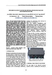
Figure 1: THmn threshold gate. 2.2NCL Systems NCL systems, like synchronous circuits, have both combinational and registration portions. However, NCL circuits also have completion components used for generating the controlling handshake signals. Furthermore, these three components are all built from the same threshold gates. Each stage in an NCL pipeline consists of these three components: combinational logic, registration, and completion logic. In an NCL system the DATA wavefront and NULL wavefront are applied alternatively. The NULL wavefront is characterized by all the inputs being NULL, while a DATA wavefront refers to all inputs of a circuit being DATA, some combination of DATA0 and DATA1. The NCL registers interact with one another using handshaking signals and are responsible for ensuring that successive DATA wavefronts are separated by a NULL wavefront. When all outputs of a combinational circuit are DATA, request for NULL, rfn, is generated on the Ko output of the register. Similarly, request for DATA, rfd, is generated on the Ko register output when all combinational logic outputs are NULL. 2.3NCL Adder The NCL system chosen for test purposes in this paper is a 2-stage adder. Like most NCL systems, this is a pipelined system with combinational logic blocks sandwiched between NCL registration units. A block diagram of the 2-stage adder is illustrated in Figure
NCL Reg
A B Cin
In
NCL Full Adder
Out
In
Out
NCL Half Adder
2-bit
3-bit
Ko
NCL Reg
Completion Detector
Ki
Ko
Ki
NCL Reg In
Out
S Cout
2-bit
Completion Detector
Ko
Completion Detector
Ki
Ko
Ki
Figure 2: Block Diagram of the NCL Adder.
2. As shown in the figure, the adder consists of four subsystems namely – • NCL Registration Unit • Completion Detector • Full Adder • Half Adder A, B, and Cin are input to the first 3-bit NCL register. The input patterns follow the NCL paradigm. The full adder adds the three inputs A, B, Cin and produces carry and sum outputs. This is fed to the second NCL register, a 2-bit one, which then feeds these signals to the half adder. The half adder takes the two signals as its inputs and then adds them to produce carry and sum outputs. These are in turn fed to the third NCL register, which is again a 2-bit register, in order to output the results. The flow of the DATA and NULL input patterns through the system is controlled by the handshaking protocol. Note that this is an extremely simplified system, used only to demonstrate the proposed testing methodology.
3.0 Testing of Asynchronous Designs Testing asynchronous circuits has been a major challenge compared to that of testing synchronous circuits. In order to compete with the synchronous counterparts, asynchronous design methods should be capable of producing VLSI circuits which are at least as readily testable as synchronous circuits. The lack of efficient and widely accepted design and test techniques for asynchronous circuits in addition to little or no CAD support has limited the widespread use of asynchronous designs in commercial VLSI application. Synchronous testing techniques though popular and well tested cannot be directly applied to asynchronous circuits due to their inherently different composition. Several possible
solutions are being developed to tackle the above problem. One such technique, NCL, uses existing conventional CAD tools to overcome the problem. The advantage of this is that existing engineers don’t have to be re-trained to use any of the tools and ease of use could lead to widespread acceptance. NCL design methodology is a relatively new area in asynchronous design and considerable research still needs to be done. The goal of this work is to identify prospects for research on the testing and testability of NCL designs and to propose methods for improving the testability of NCL designs using conventional DFT tools. Early research attempts on delay insensitive circuits were not pursued aggressively because practical delay insensitive circuits were considered limited or impossible. Though limited in number, the research work on testability of NCL designs is a significant step in the right direction. Ivan Blunno and Luciano Lavango [10] have successfully demonstrated automated synthesis of micro-pipelines from behavioral Verilog HDL. The work by M Ligthar, K Fant, R. Smith, A Kondratyev [11] uses commercial HDL synthesis tools for asynchronous design. The ability to perform conventional synthesis and simulations in an asynchronous design marks an important step in overcoming the roadblock. 3.1Test Points Insertion Failures in VLSI circuits can be modeled at different levels of abstraction. Design-for-test CAD tools target the design at the gate-level in order to reduce the number of primitives and the complexity of computations. By doing so, the tools achieve a good correlation between actual failures at the Physical Design (PD) level of abstraction and the stuck-at-fault models at gate-level.
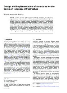
NCL Reg
A B
In
Out
Cin
NCL Full Adder
CD
TC
Ki
In
Out
NCL Half Adder
2-bit
3-bit
Ko
NCL Reg
CD
Ko
NCL Reg In
Out
S Cout
2-bit
Ki
CD
Test
Test
poi
poi
Ko
Ki
Ko
Ki
Figure 3: Improving testability by test point insertion. Controllability can be defined as the ease with which the appropriate test vector can be set at the primary inputs, to excite the fault location. Observability on the other hand, is the ease with which the excitation of the fault can be observed at a primary output node or a latch. Circuits with poor controllability and observability have suffered substantial fault coverage degradation. The technique proposed brings about increased testability by a) Increasing controllability by adding test points b) Breaking feedback loops c) Increasing observability
not have any impact on the functionality. This is more often used in synchronous circuits to improve fault coverage. In this work, to preserve the asynchronous clockless design, observation latches were not employed and test points is the highlight. Given their delay insensitive behavior, the NCL systems do not suffer any decrease in performance due to the insertion of test points.
Enhancement to testability can be achieved by inserting test points on some selective nets where faults are declared as unstable by the tools [15]. Unstable faults can be either redundant faults that exist in redundant logic or faults those are untested due to poor controllability and observability [16]. Redundant faults can be removed by removing redundant logic in the design. Feedback loops can significantly degrade stuckat fault coverage. Feedback increases the complexity of test to that of testing a sequential circuit in which two vectors are needed where t1 is the initialization vector and t2 is the test vector. Breaking feedback loops is essential in achieving high fault coverage and keeping the complexity of the test as simple as that of a combinational circuit. The NCL based asynchronous system shown in Figure 2 has several feedback loops in the control path. Feedback loops can be broken by inserting XORs controlled by an external test signal. This test signal (TC) is a primary input and it is set to ‘0’ in the functional mode and the tester controls its value in the test mode. This scheme enhances the controllability, which in turn improves the fault coverage. Test points could be observation latches added to the design observed only during the test mode to capture fault excitation when applying a test vector. These latches do
The feedback loops in the control path of the NCL adder were broken and test points were inserted for the purpose of test as shown in Figure 3. The new test model including the XORs, an external TC pin and necessary design modification was imported to the DFT tools and a fault model was created. It should be noted that both functional and test models were verified for Boolean equivalence CBool_set as explained in [1]. The registers used in the design are also composed of Thmn gates and can be converted to the equivalent Boolean form. By doing this, it is ensured that the design is in a form which can be recognized by the DFT tools library. The Boolean equivalent design thus obtained can be used with any industry standard DFT tool suite. Although breaking the feedback loops would improve the fault coverage, the inherent problem of some faults remaining untestable would still prevail. Analysis of the Automatic Test Pattern Generator (ATPG) results for this NCL adder showed that some faults were controllable but unobservable. The topology of the design with limited primary output pins prevented some fault excitations from reaching the output. The primary challenge faced in this work was to devise a scheme to enhance observability with minimum design modifications. Two schemes have been analyzed in
4.0 Implementing DFT for a Pipelined NCL Adder
Figure 4, which shows only the first stage of the twostage adder pipeline. The same was expanded on to the second stage also. The first scheme is illustrated in the first module of Figure 4, where XORs are added to the untestable fault locations and the outputs are brought out to the primary output pins. Although observability is greatly enhanced with this method, design complexity also increases tremendously, due to the addition of one primary output pin for each observation point added. This not only leads to undesirable increase in cost of adding additional output pins to the chip but the long wire connections also make the design susceptible to signal coupling and physical defects such as bridging faults. Having a huge number of outputs switching at the same time could cause EMI problems of ground bounce and SSN which can be difficult to model and analyze.
The second solution strives to limit the number of added observation points at the primary output pins to a single point. This was accomplished by consolidating the observation points with the inclusion of a balanced XOR tree structure as seen in the second module of Figure 4. Other than reducing the number of primary output pins and the routing of long wires, the second scheme also shortens the length of a signal path in the design from an input edge, where all the test values are approximately equally likely to an observation primary output pin. In terms of cost, the resulting scheme would add a single test pin, one output pin and a few XOR gates. The delicate tradeoff between yield and cost is reached. Yet another advantage of this method is that Weighted Random Pattern Test (WRPT) can effectively be run as a result of less probability of having random resistance
faults. Furthermore, the presence of random resistance faults degrades random testing, which is beyond the scope of this paper.
5.0 Results and Analysis The testing methodology as discussed in the previous sections was applied to the NCL adder circuit. VHDL was used for design capture using structural level gate modeling. The NCL designs were converted to their equivalent Boolean sets using the ATPG library components. These designs were then fed to Mentor Graphics FastScan, which performs full scan and scan sequential ATPG. In this section, the results obtained by inputting the VHDL structural descriptions of the design at different stages of testing have been discussed in detail. Table 2 highlights the fault coverage obtained for individual entities and pipelines. As shown in Table 2, in the first stage of testing the various modules in the NCL adder were individually tested using FastScan and their fault coverage was observed. The half and full adders directly yielded 100% fault coverage, whereas the register had a low coverage initially, due to the presence of some redundant logic. The design was carefully parsed to remove the redundant gates and the coverage increased to 100%. A single stage pipeline, consisting of the full adder sandwiched between two registers, was tested separately. Cases 4 and 5 represent the fault coverage for the single and double stage pipelines without adding the test methodology discussed in 4.0. As
can be seen, the fault coverage is very low in both cases and this is due to the feedback. When there is just one feedback path (Case 4), the coverage is 53% with 60 faults. When the number of feedback paths was increased to two, the coverage dropped by half and became 27.8% and the number of untestable faults increased by more than two-fold to 143. Clearly, the motivation for this paper is justified because the presence of a couple of feedback paths in the design debilitates the testability drastically as it is very difficult to control these paths. By adding a TC pin that is ‘0’ during normal operation and ‘1’ during test mode, and inserting a test point in the single feedback path of Case 4, the coverage of the single stage pipeline became 98.24%. The insertion of one observation point can also be seen. This was done to observe a long path through the design which proved to be unobservable. Case 7 shows similar results for the two-stage pipeline also, but the number of untestable faults is 9. The suspected cause for these faults was that some of the long paths were becoming unobservable. Controllability is taken care of due to the inclusion of the XOR gate. In order to check this, Case 8 was tried, where 8 observation points were included at the points where the untestable faults were diagnosed as described in the first module of Figure 4. This yielded a very high coverage of 99% and 1 untestable fault, confirming that the problem at hand was observability. As a next step, the 8 observation points were condensed to 1 observation point at the output by using an XOR tree, without actually balancing it. The coverage dropped lower than Case 7 to 97.63% with 6 untestable faults. After carefully balancing the XOR tree
Table 2 – Simulation Results Case
System under test
Before Application of XORs 1 Full Adder
Fault Coverage
Untestable Faults
# of test points
# of observation points
100%
Nil
0
0 0
2
Half Adder
100%
Nil
0
3
n-bit register
100%
Nil
0
0
4
Pipeline with depth = 1
53%
60
0
0
5
Pipeline with depth = 2
27.80%
143
0
0
98.24%
3
1
1
98.09%
9
1
2
99%
1
2
8
97.63%
6
1
1
99.03%
5
1
1
After Application of XORs 1-Stage pipeline (Case 4) 6 with XOR insertion 2-Stage pipeline (Case 5 ) 7 with XOR insertion Case 7 with 8 observation 8 points and 1 more test point After Introducing XOR trees Case 8 with unbalanced 9 XOR trees Case 9 with Balanced 10 XOR trees
in Case 10, by making sure the nets which had equal probability of transitioning were at the inputs to each XOR gate, the coverage increased to 99.03%, which is same as the one in Case 7. The 5 untestable faults that remain are 4 unobserved and 1 ATPG untestable fault. It is difficult to eliminate this fault because the probable reason for the occurrence of this fault is some instability in the algorithm adopted by the ATPG.
6.0 Conclusion and Future Work This paper presents an efficient Design for test approach employed for a pipelined NCL adder with stuck-at-fault coverage exceeding 99%. The challenge was to enhance fault coverage with test points’ insertion maintaining the pure clockless nature of the asynchronous design. A balanced XOR chain was employed to increase observability by adding only one primary output pin. With careful Physical Design (PD), minimizing the impact of adding the XOR tree can be achieved easily without degrading functional behavior. An appropriate future work to this would be to consider the gate internal feedbacks. We propose to use the same testing methodology of the insertion of the XOR gate in the feedback path present in the threshold gates in order to satisfy the hysterisis condition.
References [1] S. Hauck, “Asynchronous Design Methodologies: An Overview”, IEEE Jan 1995. [2] S. H. Unger, Asynchronous Sequential Switching Circuits, Wiley, New York, 1969 [3] A. J. Martin, “Programming in VLSI”, Development in Concurrency and Communication, Addison-Wesley, pp. 1-64, 1990. [4] S. M. Nowick, D. L. Dill, “Synthesis of Asynchronous State Machines Using a Local Clock”, Proc., ICCAD, pp. 192-197, 1991. [5] S. C. Smith, Gate and Throughput Optimizations for NULL Convention Self-Timed Digital Circuits, Ph.D. Dissertation, School of Electrical Engineering and Computer Science, University of Central Florida, 2001. [6] C. J. Myers, Asynchronous Circuit Design, Wiley publications, USA, Jul 2001 [7] I. Blunno, L. Lavagno, “Automated synthesis of micropipelines from behavioral Verilog HDL”, Proc. International Symposium on Advanced Research in Asynchronous Circuits and Systems, IEEE, Apr 2000 [8] M. Ligthart, . Fant, R. Smith, A. Taubin, A. Kondratyev, “Asynchronous design using commercial HDL synthesis tools”, Proc. International Symposium on Advanced Research in Asynchronous Circuits and Systems, IEEE, Apr 2000. [9] W. K. Al-Assadi et. al, “Faulty Behavior of Storage Elements and it Effects on Sequential Circuits”, IEEE Transactions on VLSI Systems, Vol. 1, no. 4, pp 446-
452, Dec 1993 [10] M. L. Bushnell, A. D. Agrawal, “Essentials of Electronic Testing for Digital, Memory and Mixed Signal VLSI Circuits”, Kluwer Academic Publishers, 2001. [11] A Kondratyev, L Sorensen, A Streich, “Testing of Asynchronous Designs by Inappropriate Means. Synchronous approach.” IEEE 2002. [12] “A proposal for Research on Testability of Asynchronous Circuits”, Internal report HPCA-ECS95/03, Aug 1998. [13] Roig, Formal Verification and Testing of Asynchronous Circuits, Ph.D. Dissertation, Universitat Politecnica de Catalunya, May 1997. [14] Y-S Kang, K. H. Huh and S. Kang, “New Scan Design of Asynchronous Sequential Circuits”, Dept. of Electrical Eng., Yonsei University. [15] S. K. Bandapati, S. C. Smith, M. Choi, “Design and Characterization of NULL Convention Self-Timed Multipliers”, IEEE Design and Test of Computers: Special Issue on Clockless VLSI Deign, Nov 2003. [16] M. Kishinevsky, A. Kondratyev, L. Lavagno, A. Taubin, “Partial-Scan Delay Fault Testing of Asynchronous Circuits”, IEEE, Nov 1998.