gated implementation issues speci c to adiabatic system development and ..... Adiabatic computing with the 2N-2N2D logic family. In 1994. International ...
Implementing and Evaluating Adiabatic Arithmetic Units Micah C. Knapp
Peter J. Kindlmann
�
Marios C. Papaefthymiou
Department of Electrical Engineering Yale University New Haven, CT 06520
Abstract
of their energy consumption. When simulated at operating frequencies of 10MHz and 33MHz, our arithmetic In recent years, several adiabatic logic architectures units achieved energy savings factors of 4 and 3, respechave been proposed for low-power VLSI design. However, tively. The remainder of this paper has ve sections. In Secno work has been presented describing the implementation and evaluation of nontrivial adiabatic circuits. We tion 2 we brie y present a few adiabatic logic structures, have evaluated a speci c adiabatic architecture and used and in Section 3 we discuss the logic-level implementait in the design of low-power arithmetic units. We investi- tion issues associated with the architecture we used in our gated implementation issues speci c to adiabatic system designs. In Section 4 we describe our designs and discuss development and performed a systematic comparison of related system-level implementation issues. In Section 5 our designs with corresponding CMOS circuits. In this we present the results of our empirical comparison. We paper we describe our adiabatic designs, discuss imple- conclude with a discussion of possible target systems for mentation issues at the logic and architectural level, and adiabatic implementation. report our empirical ndings.
1. Introduction
2. Adiabatic logic families
Researchers have proposed several adiabatic logic architectures. A family of structures based on reversible logic has been described in [6, 7]. An architecture inspired by bipolar transistor structures has been proposed in [3]. Two fairly simple adiabatic architectures based on diodes have been presented in [1, 2], and an extension of these structures that uses cross-coupled p-type transistors instead of diodes has been described in [4]. Inverters from the last three logic families are shown in Figure 1 and are named by the number and types of devices needed to generate them. Our empirical study covered the structures in Figure 1 and focused on the 2N2P architecture with two NMOS and two PMOS transistors in its inverter. All of these adiabatic structures are dynamic, that is, the input clock provides the energy that drives the output loads of each gate. The adiabatic logic families we studied require either two or four clock phases for their operation, with relative shifts of 180o or 90o , respectively. These clocks can be sinusoidal and can be driven from free-running oscillators. Our simulations of simple adiabatic structures and [1, 2, 4] indicated that the most important operational characteristics for the successful utilization of adiabatic logic architectures are a constant load presented by the gates to the clock, the reduction or elimination of oating output nodes, the ability to generate a signal and its complement on the same clock phase, the reduction of the � This work was supported in part by a Young Investiganumber of clock phases needed for correct operation, the tor Award from the US Army Research O�ce under Grant No. ability to drive a high output to Vdd and a low output to DAAH04-95-1-0281. Vss , predictable operation under normal operating conLow-power circuit design methodologies based on the thermodynamic principle of adiabatic changes have received considerable attention in recent years. Adiabatic circuits achieve low energy consumption by maintaining small potential di�erences across their devices while they are conducting and by allowing the energy stored in their capacitors to be recycled. Energy is supplied periodically to the gates of an adiabatic circuit by means of slowly changing clocking waveforms. These waveforms are driven by oscillators which recycle the energy stored in the circuit's capacitors. Despite the development of several adiabatic logic architectures, there exist no reports on the di�culties associated with the development of nontrivial adiabatic circuits or on the actual power savings that have been achieved by nontrivial adiabatic circuits. We recently performed an empirical study of several adiabatic logic structures that have been proposed in the literature. We focused our investigation on the logic architecture described in [4] and we used it to design adiabatic adders and multipliers with low energy dissipation. In this paper we describe our designs and discuss related logic and architectural level implementation issues such as transistor sizing, data synchronization, latency, and throughput. We also present an empirical comparison of our designs with corresponding CMOS designs in terms
1T1D
2N-2N2D OUT_b OUT
OUT_b IN IN_b IN
Φ
Φ 2N2P
Φ
x OUT_b IN
y OUT IN_b
Figure 1: Adiabatic inverters with and without diodes. ditions, and the reduction or elimination of diodes. No single logic family covered all of these requirements, but we found that the 2N2P devices covered more than the other structures.
3. Logic-level issues concerning 2N2P
Figure 2: Fault in an incorrectly ratioed 2N2P inverter. both PMOS transistors x and y turn on and start conducting. The drain of one of the two PMOS transistors, for example x, is connected to ground through a tree of NMOS gates, and its output OUT b is thus forced to \low". Due to the cross-coupling of OUT and OUT b, transistor y remains on and turns x o� when the voltage of signal OUT exceeds the PMOS threshold voltage. The problem arises when the PMOS transistors are too strong with respect to the NMOS tree, in which case the output OUT b that should be forced to ground through the NMOS tree is driven to the PMOS threshold value via x. When this occurs, the output OUT b is forced to the wrong state. Figure 2 illustrates the logic fault that can occur with a 2N2P logic inverter. The top graph shows the input data. The middle graph shows the output waveform of a correctly functioning 2N2P inverter, where the PMOS width is 20�, the NMOS width 3�, and the output load is 100fF. The bottom graph shows the output of a 2N2P inverter exhibiting a functional fault (the second output should be at \0" instead of \1"). In this case, the PMOS width is 30�, the NMOS width is 3�, and the output load is 100fF. To prevent this logic fault, we can recommend, that the NMOS logic trees be kept fairly small, that is, not many NMOS transistors in series between the output and ground, and that the PMOS transistors are kept fairly \weak" with respect to the NMOS transistors. Unfortunately, \weak" PMOS transistors connect the output loads to the input clock through a large resistance, and therefore, increase the energy consumed by the gate. These factors must be considered and balanced correctly to build a functional, low-power 2N2P logic gate. The 2N2P logic gates must be used with caution, and large circuits built with this logic family must be thoroughly simulated with accurate load estimates to ensure a functional circuit.
The 2N2P logic family is very similar to CMOS CVSL logic [5] and thus possesses several of the positive characteristics of conventional CMOS. Since 2N2P gates use ground nodes and avoid diodes, they can drive their output loads to Vdd and Vss . Also, for at least some portion of the clock cycle, the outputs of the 2N2P gates are not oating and, therefore, are much less susceptible to noise. The 2N2P logic gates generate both the output signal and its complement on the same clock phase and can use the di�erential signal pairs to generate fairly complex logic functions such as XOR in one gate. Another bene t of generating both a signal and its complement from the same gate is that the load \seen" by the input clock is relatively the same regardless of what output level is being driven. This balanced load prevents the clock oscillator from changing frequency due to shifts in the capacitance of the circuit. Even though they are connected to the ground, the 2N2P logic gates can recycle a large percentage of the energy used to charge their output nodes. Unfortunately, the 2N2P logic family has some potentially serious problems. The logic gates cannot hold an output value for more than a quarter of the clock cycle and, therefore, require four clocks to build logic circuits. Moreover, the 2N2P logic gates use a ratioed gate structure such that the PMOS and NMOS transistors must be sized according to the output load and to each other. If an incorrect ratio is used, a logic fault may occur which, in addition to driving an incorrect output value, causes the gate to consume signi cant amounts of energy. We looked closely at the logic fault that can occur with 2N2P, and discovered that it is caused by the manner in which the logic gates evaluate their output levels. We 4. Systems implementation issues describe the events which force a logic fault to occur in We have used 2N2P logic gates to design two adiabatic terms of the 2N2P inverter (as shown in Figure 1). When the input clock � reaches the PMOS threshold voltage, circuits of medium complexity, a 4x4 bit carry lookahead
X
X
X
X
5.5
Y
5 4.5
P HA
HA
3.5
P Y FA
FA
FA P Y
FA
FA
Power (uW)
HA
ADL CMOS
4
Y
3 2.5 2 1.5
FA 1
P 0.5
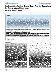
3-bit Carry Look Ahead Adder
P
P
P
P
Figure 3: 4x4 bit adiabatic multiplier. adder with about 200 transistors and a 4x4 bit multiplier (shown in Figure 3) with about 500 transistors. Both circuits assume parallel data in and out, have been extensively simulated using Hspice and function correctly. We have also designed larger circuits, an 8x8 bit carry lookahead adder with about 700 transistors and an 8x8 bit multiplier with approximately 2500 transistors, which also appear to be functionally correct based on preliminary simulations. For all designs we used MOSIS 1�m process technology with Vdd = 3 Volts and minimum-size transistors (l=w = 3�=2�, where � = :5�m). We have identi ed three important system design issues with 2N2P that are mostly applicable to system design with any adiabatic logic family. The rst issue is that adiabatic circuits have limited potential to achieve both signi cant energy savings and high performance. One of the largest performance limiting factors is that the dynamic gates in an adiabatic circuit can only perform one logic evaluation per clock cycle. Since the gate clock frequencies must be slow to achieve savings in energy consumption, the overall circuit speed can be very slow. For example, consider an adiabatic circuit consisting of four cascaded logic gates. The latency of this circuit is 100ns, assuming a 10MHz gate clock frequency. The upper bound on the throughput is 10MHz (that is, new input data every 100ns), since each gate in the circuit can analyze new data only once per cycle. Since 2N2P circuits have large latencies and relatively low throughputs, each gate must perform as complicated a function as possible in order to increase system performance. In Section 3, however, we saw that a long and weak NMOS tree can lead to logic faults with 2N2P. Thus, the complexity of the functions that can be performed reliably by any gate without excessively increasing its size and energy consumption is limited. Another critical system issue that stems from the dynamic nature of the adiabatic gates is data synchronization. Since every gate introduces a phase delay from input to output, two signals that originate from di�erent clock phases must be synchronized in order to be used as inputs to the same adiabatic gate. This requirement leads to the insertion of data bu�ers, each of which shifts a signal by one phase (a quarter clock period). A large
5
10
15
20 25 Frequency (MHz)
30
35
40
Figure 4: Power vs frequency for 4x4 bit adders. number of additional gates are thus added into the circuit just to maintain data synchronization. For example, our 4x4 bit adiabatic multiplier requires the addition of 25 data bu�ers to maintain data synchronization. These bu�ers are denoted as thick black lines in the block diagram of our 4x4 adiabatic multiplier shown in Figure 3. An adiabatic logic family that only requires two clocks (where each gate introduces a half clock period delay) would require fewer data bu�ers but would get less work done per period, since only two logic functions could be performed per clock period. Every adiabatic logic family we investigated uses mostly analog signals to perform digital functions, thus allowing the logic to recycle energy and limit the power dissipated by the circuit. Unfortunately, it is impossible to simulate such systems with simple digital simulators. More complex analog simulators such as Hspice must be used to not only test critical circuits and special \corner cases", but also to test the functionality of the circuit. For more complex circuits, the computing requirements can be very high. For example, simulations of our 4x4 multiplier with 256 input test vectors take on the order of 4 hours to complete using Hspice on a state of the art PowerPC-based workstation with 64MB main memory. Since adiabatic systems must be thoroughly tested to ensure correct functionality, large scale development of adiabatic systems can be very expensive in terms of time and resources.
5. Systems evaluation
We compared the energy consumption of our adiabatic arithmetic units with that of equivalent CMOS circuits that we designed for minimum energy consumption. The input data rates for the CMOS circuits were identical to those for the adiabatic circuits, and therefore, our comparison was based on energy consumed per computation (the circuits did equal amount of computing during equal amounts of time). We reduced the amount of glitching in the CMOS circuits using standard CMOS design techniques. Since the energy consumed per operation in a CMOS circuit can be approximated by C Vdd2 , we used minimum sized transistors in all CMOS gates in order to minimize the overall circuit capacitance. Figures 4 and 5 show the energy consumption per clock �
10 9 ADL CMOS
8
Power (uW)
7 6 5 4 3 2 1 5
10
15
20 25 Frequency (MHz)
30
35
40
Figure 5: Power vs frequency for 4x4 bit multipliers.
Figure 7: Latency in 4x4 bit CMOS multiplier. adiabatic adder is 4 clock phases, and the latency of our adiabatic multiplier is 12 clock phases.
6. Conclusion
Large scale system development using adiabatic technologies is more complex than conventional CMOS circuit development because of data synchronization and simulation issues. Moreover, adiabatic circuits have large latencies due to the dynamic nature of their gates. Another subtle yet important performance issue with adiabatic systems is that although it is possible to build adiabatic memory elements, these elements have a latency of one clock cycle. Therefore, they can only be clocked at a maximum frequency of half the gate clock frequency. The implication of this fact is that the clock frequencies speci ed by default for adiabatic and CMOS circuits are not directly comparable, since the former usually refers to gate frequencies, and the latter refers to Figure 6: Latency in 4x4 bit adiabatic multiplier. system frequencies. Therefore, it seems that adiabatic technology is more cycle for our 4x4 carry lookahead adders and 4x4 multipliers, respectively. The graphs were obtained from suitable for low-speed, combinational circuits. Hspice simulations of 256 test vectors at data rates of References 10, 16, 25, and 33MHz. Our adiabatic circuits exhibit signi cant savings in energy consumption, especially at [1] J. Denker, S. Avery, A. Dickinson, A. Kramer, and T. Wik. low clock frequencies. At 10MHz the relative savings facAdiabatic computing with the 2N-2N2D logic family. In 1994 tor is 4, and at 33MHz the relative savings factor is 3. International Workshop on Low Power Design, April 1994. Preliminary simulations of our 8x8 bit designs indicate [2] A. Dickinsonand J. Denker. Adiabatic dynamic logic. In CICC, 1994. power savings similar to those achieved with the 4x4 bit [3] R. Hinman and M. Schlecht. Recovered energy logic: A highly circuits. e�cient alternative to today's logic circuits. In IEEE Power Figures 6 and 7 illustrate the performance issues in Electronics Specicalists Conference Record, pages 17{26, 1993. adiabatic systems design. Figure 6 illustrates the latency [4] A. Kramer, J.S~. Denker, B. Flower, and J. Mulrony. 2nd order adiabatic computation with 2N-2P and 2N-2N2P logic circuits. of our 4x4 bit adiabatic multiplier running at 33Mhz. In 1995 International Workshop on Low Power Design, April The top graph shows one of the four gate clocks, the 1995. middle graph shows the input, and the bottom graph [5] N. Weste and K. Eshraghian. CMOS VLSI Design. Addisonshows the output which is lagging ve phase delays after Wesley, Reading, Massachusetts, 1985. the input signal. When compared with CMOS, adiabatic [6] S. Younis and T. Knight. Practicalimplementationof charge recovering asymptotically zero-power CMOS. In Research in Incircuits su�er from very long latencies. In Figure 7, the tegrated Systems: Proceedings of the 1993 Symposium, March top graph shows the input and the bottom graph shows the output for the CMOS multiplier. In this circuit, the [7] S.1993. Younis and T. Knight. Asymptotically zero energy split-level input/output latency is 8ns and the e�ective throughput charge recovery logic. In Proceedings of the 1994 International Workshop on Low Power Design, March 1994. can reach 125MHz. Our 4x4 adder has a latency of 3 clock phases, which is still much more signi cant than that of the CMOS adder. For the 8x8 bit designs, the di�erences are even more signi cant. The latency of our