energies Letter
Inductive Power Transfer Systems for Bus-Stop-Powered Electric Vehicles Chung-Chuan Hou * and Kuei-Yuan Chang Department of Electrical Engineering, Chung Hua University, Hsinchu 30012, Taiwan;
[email protected] * Correspondence:
[email protected]; Tel.: +886-3-518-6351 Academic Editor: Chunhua Liu Received: 20 February 2016; Accepted: 20 June 2016; Published: 30 June 2016
Abstract: This study presents an inductive power transfer (IPT) system for electric vehicles (EVs) based on EE-shaped ferrite cores. The issues of the IPT system such as efficiency, air gap, displacement, dislocation, and motion are discussed. Furthermore, finite element analysis software is utilized to simulate the IPT system operated under large air gap conditions. Simulation and measurement results are presented to validate the performance of the proposed scheme and meet the requirements for bus-stop-powered EVs. Keywords: inductive power transfer; bus-stop-powered; electric vehicles
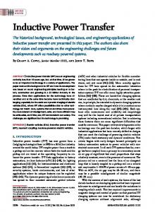
1. Introduction As the air pollution problems caused by gasoline-powered vehicles have become more and more serious, electric vehicles (EVs) [1–3] or hybrid EVs have been regarded as good solutions and gained increasing attention. However, the batteries used in EVs or hybrid EVs have some significant disadvantages, such as high cost and heaviness, limited capacitance and charging/discharging cycles, and long charging time, etc. The roadway-powered EVs [4–8] scheme has therefore been discussed to reduce the battery capacitance and to extend the driving range. This study would like to furthermore present the inductive power transfer (IPT) system [9–13] for bus-stop-powered EVs [14] with much less cost than the roadway-powered EVs system. Figure 1 shows the IPT system for bus-stop-powered EVs or hybrid EVs. The active front-end (AFE) converter is utilized as interface between the AC voltage grid and DC voltage grid. The advantages of the AFE converter are bidirectional power flow and low total harmonic distortion (THD) of the line current. The primary side of the IPT system is DC-AC H-bridge inverters. The multi-H-bridge inverters are utilized to increase the transfer power and efficiency of the IPT system. The secondary side of the IPT system is a pick-up coil and receiver built in the EVs or hybrid EVs. The IPT receiver is utilized to charge up battery or supply power to motor through the inverter. The IPT system for moving EVs or hybrid EVs is convenient for charging up battery and could also extend driving range. Furthermore, the position regulation sensors of the IPT system are utilized to control the operation of multi-H-bridge inverters and improve the efficiency of the IPT system.
Energies 2016, 9, 512; doi:10.3390/en9070512
www.mdpi.com/journal/energies
Energies 2016, 9, 512 Energies 2016, 9, 497
22 of 14 of 14
Energies 2016, 9, 497
2 of 14
Bus Bus stop stop
Battery Battery
IPT Receiver IPT Receiver
Inverter Inverter
Motor Motor
IPT IPT H-bridge H-bridge Inverter Inverter
AFE AFE
Figure 1. Inductive power transfer system for bus‐stop‐powered EVs or hybrid EVs. Figure 1. Inductive power transfer system for bus‐stop‐powered EVs or hybrid EVs. Figure 1. Inductive power transfer system for bus-stop-powered EVs or hybrid EVs.
2. Inductive Power Transfer System 2. Inductive Power Transfer System 2. Inductive Transfer Figure Power 2 shows the System simplified IPT system based on EE‐shaped ferrite cores for Figure 2 shows the simplified IPT system based on EE‐shaped ferrite cores for bus‐stop‐powered EVs or hybrid EVs. As shown in Figure 2a, the DC bus voltage is V dc, the DC‐AC Figure 2 shows the simplified IPT system based on EE-shaped ferrite cores for bus-stop-powered bus‐stop‐powered EVs or hybrid EVs. As shown in Figure 2a, the DC bus voltage is V dc , the DC‐AC H‐bridge inverter is utilized to generate the high frequency square wave voltage Vin. The EE‐shaped EVs or hybrid EVs. As shown in Figure 2a, the DC bus voltage is Vdc , the DC-AC H-bridge inverter H‐bridge inverter is utilized to generate the high frequency square wave voltage Vin. The EE‐shaped ferrite cores are utilized to transfer the power to secondary side load (by pick‐up coil and receiver). is utilized to generate the high frequency square wave voltage Vin . The EE-shaped ferrite cores are ferrite cores are utilized to transfer the power to secondary side load (by pick‐up coil and receiver). The primary inductance and secondary inductance are Lp and Ls. The mutual inductance is M (=Lm). utilized to transfer the power to secondary side load (by pick-up coil and receiver). The primary The primary inductance and secondary inductance are Lp and Ls. The mutual inductance is M (=Lm). The coupling coefficient (k) is defined as in (1): inductance and secondary inductance are Lp and Ls . The mutual inductance is M (=Lm ). The coupling The coupling coefficient (k) is defined as in (1): coefficient (k) is defined as in (1): M k M (1) M (1) kk “ ? LLPPLLSS (1)
LP LS
As cores are are A B (38 (38 mm), mm), As shown shown in in Figure Figure 2b, 2b, the the dimensions dimensions of of the the EE-shaped EE‐shaped cores A (80 (80 mm), mm), B C (20 mm), D (28 mm), E (59 mm), F (20 mm), G (F/2), H (E/2–F/2), and I (A/4–E/4). The material As shown in Figure 2b, the dimensions of the EE‐shaped cores are A (80 mm), B (38 mm), C (20 mm), D (28 mm), E (59 mm), F (20 mm), G (F/2), H (E/2–F/2), and I (A/4–E/4). The material of of the EE-shaped cores is 3C90 made by Ferroxcube (NewTaipei TaipeiCity, Taiwan, City, Taiwan, R.O.C.). R.O.C.). The C (20 mm), D (28 mm), E (59 mm), F (20 mm), G (F/2), H (E/2–F/2), and I (A/4–E/4). The material of the EE‐shaped cores is 3C90 made by Ferroxcube (New The relative relative ´ 7 −7 H/m). permeability space: 4π4π ˆ× 1010 Figure 2c the equivalent the EE‐shaped cores is 3C90 made by Ferroxcube (New Taipei City, Taiwan, R.O.C.). The relative permeability is is 2300 2300 (permeability (permeability ofof free free space: H/m). Figure 2c shows shows the equivalent −7 resonant circuit of the primary series resonant and secondary parallel (SP) topology IPT system and permeability is 2300 (permeability of free space: 4π × 10 H/m). Figure 2c shows the equivalent circuit of the primary series resonant and secondary parallel resonant (SP) topology IPT system and Figure 2d shows the secondary parallel resonant (P) topology IPT system, respectively. circuit of the primary series resonant and secondary parallel resonant (SP) topology IPT system and Figure 2d shows the secondary parallel resonant (P) topology IPT system, respectively. Figure 2d shows the secondary parallel resonant (P) topology IPT system, respectively.
(a) (a)
(b) (b)
(c) (c)
(d) (d)
Figure 2. Simplified inductive power transfer system. (a) Circuit of the IPT system; (b) EE‐shaped Figure 2. Simplified inductive power transfer system. (a) Circuit of the IPT system; (b) EE-shaped Figure 2. Simplified inductive power transfer system. (a) Circuit of the IPT system; (b) EE‐shaped cores; (c) Equivalent circuit of the SP topology; (d) Equivalent circuit of the P topology. cores; (c) Equivalent circuit of the SP topology; (d) Equivalent circuit of the P topology. cores; (c) Equivalent circuit of the SP topology; (d) Equivalent circuit of the P topology.
Energies 2016, 9, 512
3 of 14
The mutual inductance is M (=Lm ) and the equivalent resistance of core loss is Rm . The primary and secondary leakage inductances are Llp and Lls as in (2). Llp “ p1´kqLp , Lls “ p1´kqLs
(2)
The primary and secondary resistances are rp and rs . The load is simplified as RL . The primary series resonant capacitor is CP and the secondary parallel resonant capacitor is Cs. The transfer function of the SP topology IPT system is given as in (3): νout psq s2 ˆ CP ˆ Lm ˆ R L {rRm ˆ pR L ` rS qs “ 2 νin psq p1 ` psH q ˆ p1 ` ω2ζ 1 s ` ωs2 q ˆ p1 ` ω2ζn22 s ` n1
n1
(3)
s2 2 q ωn2
The pole (s = ´PH ) operated at the high frequency domain is as in (4): p H “ Rm ˆ p
1 1 1 ` ` q Ll p Lls Lm
(4)
The complex-conjugate poles operated at the low frequency domain are as in (5): s “ ´pζ 1 ˘ j
b 1 ´ ζ 12 qωn1
(5)
b where the damping ratio is ζ 1 “ r P CP ωn1 {2, natural undamped frequency is ωn1 “ 1{CP pLl p ` Lm q b and resonant frequency is ωr1 “ 1 ´ ζ 12 ωn1 , respectively. The complex-conjugate poles operated at the middle frequency domain are as in (6): s “ ´pζ 2 ˘ j
b 1 ´ ζ 22 qωn2
(6) d
where the damping ratio is ζ 2 “ 1{2R L CS ωn2 , natural undamped frequency is ωn2 “
p1`rS { R L q
Ll p ˆLm
CS p Lls ` L
`Lm q
lp b 2 and resonant frequency is ωr2 “ 1 ´ ζ 2 ωn2 , respectively. According to (3), the transfer function of the IPT system with P topology is reduced as in (7):
νout psq s ˆ Lm ˆ R L {pr P ˆ pR L ` rS qq “ 2 νin psq p1 ` psL q ˆ p1 ` psH q ˆ p1 ` ω2ζn22 s ` ωs2 q
(7)
n2
The high frequency pole (s = ´PH ) is as in (4) and the low frequency pole (s = ´PL ) is as in (8): p L “ r P {pLl p ` Lm q
(8)
The complex-conjugate poles operated at the middle frequency domain are as in (9): s “ ´pζ ˘ j
b 1 ´ ζ 2 qωn
(9) d
where the damping ratio is ζ “ 1{2R L CS ωn , natural undamped frequency is ωn “
p1`rS { R L q
Ll p ˆLm
CS p Lls ` L
`Lm q
lp a 2 and resonant frequency is ωr “ 1 ´ ζ ωn , respectively. According to (3) and (7), there are two pairs of resonant poles in the SP topology IPT system and one pair of resonant poles in the P topology IPT system.
Energies 2016, 9, 512 Energies 2016, 9, 497
4 of 14 4 of 14
3. Frequency Response of the IPT System 3. Frequency Response of the IPT System The parameters parameters of of the the IPT IPT system system are are as as follows: follows: the inductance and and secondary secondary The the primary primary inductance inductance are Lp (325 μH) and Ls (325 μH). The primary series resonant capacitor is C P (0.2 μF) and inductance are Lp (325 µH) and Ls (325 µH). The primary series resonant capacitor is CP (0.2 µF) the secondary parallel resonant capacitor is Cs (0.2 μF). The resistances r p and r s are 0.72 Ω. The load and the secondary parallel resonant capacitor is Cs (0.2 µF). The resistances rp and rs are 0.72 Ω. The resistance R L is 100 Ω. load resistance RL is 100 Ω. Figure 33 shows shows the the frequency response of the IPT system on EE‐shaped cores with Figure frequency response of the IPT system basedbased on EE-shaped cores with varied varied air gap (fsw: 10–100 kHz). In SP topology, the resonant frequencies ω r1 and ω r2 move to each air gap (fsw: 10–100 kHz). In SP topology, the resonant frequencies ω r1 and ω r2 move to each other as other the air gap is increased as shown 3a. in Figure 3a. In P topology, resonant value is the airas gap is increased as shown in Figure In P topology, the resonantthe peak value ispeak decreased as decreased as the air gap is increased as shown in Figure 3b. Therefore, the SP topology is suitable the air gap is increased as shown in Figure 3b. Therefore, the SP topology is suitable for a large air gap for a large and air gap IPT system suits and athe P topology suits a small gap IPT system. The IPT system the P topology small air gap IPT system. Theair coupling coefficient and coupling resonant coefficient and resonant frequency of the IPT system with varied air gap are given in Table 1. frequency of the IPT system with varied air gap are given in Table 1. Table 1. Coupling coefficient and resonant frequency of the IPT system with varied air gap. Table 1. Coupling coefficient and resonant frequency of the IPT system with varied air gap.
Gap Llp Lls Lm k ωr1 ωr2 ωr
Llp Lls Lm k ω r1 ω r2 ωr
5 mm 5 mm 217.7 μH 217.7 µH 217.7 μH 217.7 µH 107.3 μH 107.3 µH 0.33 0.33 15 kHz 15 kHz 23 kHz 23 kHz 20 kHz 20 kHz
10 mm 10 mm 237.2 μH 237.2 µH 237.2 μH 237.2 µH 87.8 μH 87.8 µH 0.27 0.27 17 kHz 17 kHz 22 kHz 22 kHz 20 kHz 20 kHz
Bode Diagram
M agn itu de (abs)
6 4
10mm Gap:5mm
2
Bode Diagram
1.5
90
-45
0
10
10mm
0.5 00
-90
Gap:5mm
1
1800
-180 1 10
20 mm 282.7 μH 282.7 282.7 μH µH 282.7 µH 42.3 μH 42.3 µH 0.13 0.13 20 kHz 20 kHz 20 kHz 20 kHz 20 kHz 20 kHz 20 mm
2
20mm
P h ase (deg)
P h ase (deg)
M agn itu de (abs)
8
Gap
20mm
-90 -135 -180 1 10
2
Frequency (kHz)
10
2
Frequency (kHz)
(a)
(b) 200
200 20mm 150
150 Pout(W )
Pin(W )
20mm 100
100
10mm 50
0 1 10
5mm
Frequency(kHz)
50
10
2
0 1 10
(c) Figure 3. Cont.
10mm 5mm
Frequency(kHz)
10
2
Energies 2016, 9, 512 Energies 2016, 9, 497
5 of 14 5 of 14
14
14
12
12
5mm
10
8 6
Po u t(W )
P in (W )
10
10mm
4 2 01 10
5mm
8 6
10mm
4
20mm
2
Frequency(kHz)
10
2
01 10
20mm
Frequency(kHz)
10
2
(d) Figure 3. Frequency response of the IPT system based on EE‐shaped cores with varied air gap. (a) SP Figure 3. Frequency response of the IPT system based on EE-shaped cores with varied air gap. (a) SP topology (MATLAB); (b) P topology (MATLAB); (c) Input power and output power of SP topology topology (MATLAB); (b) P topology (MATLAB); (c) Input power and output power of SP topology dc: 30 V); (d) Input power and output power of P topology (test results; Vdc: 30 V). (test results; V (test results; Vdc : 30 V); (d) Input power and output power of P topology (test results; Vdc : 30 V).
Figure 3c shows the input power and output power of the SP topology IPT system with varied Figure 3c shows the input power and output power of the SP topology IPT system with varied air air gap (test results; Vdc: 30 V). The resonant frequencies of the IPT system are 15 kHz (ωr1) and gap (test results; Vdc : 30 V). The resonant frequencies of the IPT system are 15 kHz (ω r1 ) and 23 kHz 23 kHz (ωr2) under air gap 5 mm, 17 kHz (ωr1) and 22 kHz (ωr2) under air gap 10 mm, and 20 kHz (ω r2 ) under air gap 5 mm, 17 kHz (ω r1 ) and 22 kHz (ω r2 ) under air gap 10 mm, and 20 kHz (ω r1,2 ) (ωr1,2) under air gap 20 mm, respectively. The input power and output power are increased and the under air gap 20 mm, respectively. The input power and output power are increased and the efficiency efficiency is decreased as air gap increased. The measurement results of the SP topology IPT system is decreased as air gap increased. The measurement results of the SP topology IPT system are given in are given in Table 2. Figure 3d shows the input power and output power of the P topology IPT Table 2. Figure 3d shows the input power and output power of the P topology IPT system with varied system with varied air gap (test results; Vdc: 30 V). The input power, output power, and the air gap (test results; Vdc : 30 V). The input power, output power, and the efficiency are decreased as air efficiency are decreased as air gap increased. The measurement results of the P topology IPT system gap increased. The measurement results of the P topology IPT system are given in Table 2. As shown are given in Table 2. As shown in Figure 3, the measurement results agree with the simulation in Figure 3, the measurement results agree with the simulation results produced by using MATLAB. results produced by using MATLAB. Table 2. Input power, output power, and efficiency of the IPT system. Table 2. Input power, output power, and efficiency of the IPT system. 5 mm ωr1 : 5 mm ωr2 : 10 mm ωr1 : 10 mm ω r2 : 20 mm ωr1,2 : 5 mm 10 mm 10 mm 20 mm 5 mm 15 kHz ωr2: 23 kHz 23 kHz 17 kHz 22 kHz ωr1: 17 kHz ωr2: 22 kHz ω20r1,2kHz : 20 kHz ωr1: 15 kHz Input power 30 W 66 W 45 W 72 W 177 W TOPOLOGY SP TOPOLOGY Input power 30 W 66 W 45 W 72 W 177 W Output power 28 W 59.3 W 38.4 W 64 W 136.9 W Output power 28 W 59.3 W 38.4 W 64 W 136.9 W Efficiency 94% 90% 85% 89% 77% Efficiency 94% 90% 85% 89% 77% 20 mm ωr : 5 mmr: 20 kHz ωr : 20 kHz 10 mm rω GapGap 5 mm ω 10 mm ω : 20 kHz 20 mm ω r : 20 kHz 20 kHzr: 20 kHz Input power 13.2 W 7.2 W 3.9 W P TOPOLOGY Input power 13.2 W 7.2 W 3.9 W P TOPOLOGY Output power 11.9 W 5.5 W Output power 11.9 W 5.5 W 1.61.6 W W Efficiency 90% 77% 40% Efficiency 90% 77% 40% SP
Gap Gap
4. Simulation and Experimental Results 4. Simulation and Experimental Results Figure 4 shows the prototype of measurement for the P topology IPT system operated at small Figure 4 shows the prototype of measurement for the P topology IPT system operated at small air gap. The multi-H-bridge multi‐H‐bridge inverters inverters are are utilized increase transfer power efficiency of air gap. The utilized toto increase thethe transfer power andand efficiency of the the P topology IPT system as shown in Figure 4a. The X‐Z table and controller are utilized to move P topology IPT system as shown in Figure 4a. The X-Z table and controller are utilized to move the the pick‐up coil IPT and IPT receiver along the shown 4b. in The Figure 4b. The ofparameters of pick-up coil and receiver along the X-axis as X‐axis shown as in Figure parameters measurement measurement are the same as Section 3. The issues of the IPT system [13] such as efficiency, air gap are the same as Section 3. The issues of the IPT system [13] such as efficiency, air gap (Z-axis), (Z‐axis), displacement (X‐axis), dislocation (Y‐axis), and motion (X‐axis) are discussed as follow: displacement (X-axis), dislocation (Y-axis), and motion (X-axis) are discussed as follow:
Energies 2016, 9, 512 Energies 2016, 9, 497 Energies 2016, 9, 497 V dc V dc
6 of 14 6 of 14 6 of 14 i p1 i p1 V p1 V p1
C dc1 C dc1
i p2 i p2 V p2 V p2
C dc2 C dc2
IPT system IPT system
is iL is C si L V s C s Load Vs Load EE cores EE cores
i p3 i p3 V p3 V p3
C dc3 C dc3
H-bridge Inverter H-bridge Inverter
(a) (a)
(b) (b)
Figure 4. Prototype of measurement for the P topology IPT system. (a) multi‐H‐bridge inverters Figure 4. Figure 4. Prototype Prototypeof ofmeasurement measurementfor forthe the P P topology topology IPT IPT system. system. (a) (a) multi‐H‐bridge multi-H-bridgeinverters inverters (b) prototype of measurement. (b) prototype of measurement. (b) prototype of measurement.
Efficiency(%) Efficiency(%)
4.1. Air Gap 4.1. Air Gap 4.1. Air Gap Figure 5 shows the efficiency, input power, and output power of the P topology IPT system Figure 5 the efficiency, efficiency, input power, and output power of P the P topology IPT system Figure 5 shows shows the power of the topology IPTThe system based based on one H‐bridge inverter input with power, varied and air output gap and operating frequency. switching based on one H‐bridge inverter with varied air gap and operating frequency. The switching on one H-bridge variedto air100 gapkHz. and operating frequency. The5a, switching frequency (fsw) frequency (fsw) inverter is from with 10 kHz As shown in Figure for various operating frequency (fsw) is from 10 kHz to 100 kHz. As shown in Figure 5a, for various operating is from 10 kHz to 100 kHz. As shown in Figure 5a, for various operating frequencies, the IPT system frequencies, the IPT system exhibits superior performance at the resonant frequency (20 kHz). The frequencies, the IPT system exhibits superior performance at the resonant frequency (20 kHz). The exhibits superior at the resonantby frequency (20operating kHz). Thefrequency. efficiency of the IPT systemthe is efficiency of the performance IPT system is decreased increased Table 3 shows efficiency of the IPT system is decreased by Table increased operating frequency. Table 3 shows the decreased by increased operating frequency. 3 shows the efficiency, input power, and output efficiency, input power, and output power of the P topology IPT system at 20 kHz. The maximum efficiency, input power, and output power of the P topology IPT system at 20 kHz. The maximum power of the P topology IPT system at 20 kHz. The maximum efficiency of the IPT system is 93% at efficiency of the IPT system is 93% at air gap 5 mm. Figure 5b shows the efficiency, input power, efficiency of the IPT system is 93% at air gap 5 mm. Figure 5b shows the efficiency, input power, air gap 5 mm. Figure 5b shows the efficiency, input power, and output power of the IPT system with and output power of the IPT system with varied air gap from 5 mm to 65 mm (fsw: 20 kHz). The and output power of the IPT system with varied air gap from 5 mm to 65 mm (fsw: 20 kHz). The varied air gap from 5 mm to 65 mm (fsw: 20 kHz). The efficiency, input power, output power, and efficiency, input power, output power, and power loss of the IPT system are 50.9%, 49.5 W, 25.2 W, efficiency, input power, output power, and power loss of the IPT system are 50.9%, 49.5 W, 25.2 W, power lossW of (gap: the IPT 49.5 W, 25.2 24.3 W (gap: mm). The and 24.3 21 system mm). are The 50.9%, performances of W, the and P topology IPT 21system are performances increased by ofa and 24.3 W (gap: 21 mm). The performances of the P topology IPT system are increased by a the P topology IPT system are increased by a decreased air gap. decreased air gap. decreased air gap.
Pout(W) Pout(W)
Pin(W) Pin(W)
100 100 50 50 0 1 0101 10 300 300 200 200 100 1000 1 0101 10 300 300 200 200 100 1000 1 0101 10
Frequency(kHz) Frequency(kHz)
Frequency(kHz) Frequency(kHz)
Frequency(kHz) Frequency(kHz)
(a) (a)
Figure 5. Cont.
5mm 5mm 10mm 10mm 20mm 20mm 2 102 10 5mm 5mm 10mm 10mm 20mm 20mm 2 102 10 5mm 5mm 10mm 10mm 20mm 20mm 2 102 10
7 of 14
Energies 2016, 9, 497
7 of 14
Pout(W )
Pin(W )
E fficiency(% )
Energies 2016, 9, 512
100 50 0 300 200 100 0 300 200 100 0
10
20
30 40 Gap(mm)
50
60
10
20
30 40 Gap(mm)
50
60
10
20
30 40 Gap(mm)
50
60
(b) 100
10mm 15mm 20mm
Efficiency(%)
80
60
40
20
0
100
200
300
400
500
600
Load(Ohm) (c)
700
800
900
1000
Figure 5. Efficiency, input power, and output power of the P topology IPT system with varied air Figure 5. Efficiency, input power, and output power of the P topology IPT system with varied air gap gap and frequency (Vdc: 150 V; RL: 100 Ω). (a) Efficiency, input power, and output power; (b) Varied and frequency (Vdc : 150 V; RL : 100 Ω). (a) Efficiency, input power, and output power; (b) Varied air air gap from 5 mm to 65 mm (20 kHz); (c) Varied load (20 kHz). gap from 5 mm to 65 mm (20 kHz); (c) Varied load (20 kHz). Table 3. Efficiency, input power, and output power of the IPT system with varied air gap at 20 kHz. Table 3. Efficiency, input power, and output power of the IPT system with varied air gap at 20 kHz.
Air Gap (mm) Air Gap (mm) Efficiency Efficiency Input Power(W) Input Power(W) Output Power(W) Output Power(W)
5 5 93% 93% 300 300 278 278
10
20
10 85%
20 60%
85% 150 150 128 128
60% 54 54 32 32
Figure 5c shows the efficiency of the P topology IPT system with varied load 50–1000 Ω (Vdc: 150 V; Figure 5c shows the efficiency of the P topology IPT system with varied load 50–1000 Ω (Vdc : 150 V; fsw: 20 kHz). The efficiency, input power, and output power of the P topology IPT system are 85%, fsw: 20 kHz). The efficiency, input power, and output power of the P topology IPT system are 85%, 150 W, and 128 W under load 100 Ω (gap: 10 mm). The efficiency, input power, and output power 150 W, and 128 W under load 100 Ω79%, (gap:150 10 mm). The119 efficiency, input power, and output powerThe of of the P topology IPT system are W, and W under load 200 Ω (gap: 15 mm). the P topology IPT system are 79%, 150 W, and 119 W under load 200 Ω (gap: 15 mm). The efficiency, efficiency, input power, and output power of the P topology IPT system are 72%, 120 W, and 86 W input power, and output power of the P topology IPT system are 72%, 120 W, and 86 W under load under load 300 Ω (gap: 20 mm). The efficiency of the P topology IPT system is affected by the load 300 Ω (gap: 20 mm). The efficiency of the P topology IPT system is affected by the load and air gap. and air gap.
20 kHz). Table 4 shows the efficiency, input power, output power, and power loss of the IPT system. Table 4 is for displacements of 10 mm and 20 mm, respectively. The performances of the IPT system are increased by decreased displacement. Energies 2016, 9, Table 4. 512 Displacement effect of the IPT system with varied air gap from 5 mm to 40 mm 8 of 14
(fsw: 20 kHz). 5 10 15 20 25 30 35 40 Efficiency 86.8% 73.2% 61.4% 49.5% 33.3% 22.9% 14.8% 7.4% Displacement: The displacement is defined as moving the X-axis. 6 shows Input power (W) 219 along105 72 Figure 49.5 37.5 the displacement 31.5 28.5 effect 27 of 10 mm the IPT system based on one H-bridge inverter with varied air gap from 5 mm to 40 mm (fsw: 20 kHz). Output power (W) 191.1 77.2 44.1 24.5 12.5 7.2 4.2 2 Table 4 shows the efficiency, output62.7% power, 45.4% and power loss 24.2% of the IPT system. Table6.0% 4 is Efficiency input power,76.3% 33.3% 15.0% 10.6% Displacement: for displacements of 10 mm and 20 mm, respectively. the IPT 30 system are Input power (W) 97.5 64.5 The performances 46.5 37.5 of33 27 increased 27 20 mm Output power (W) 74.4 40.5 21.1 12.5 8 4.5 2.9 1.6 by decreased displacement.
Pout(W)
Pin(W)
Efficiency(%)
Displacement 4.2. Displacement Air Gap (mm)
100
10mm 20mm
50 0 5
10
15
20 25 Gap(mm)
30
35
200
10mm 20mm
100 0 5
10
15
20 25 Gap(mm)
30
35
200
40 10mm 20mm
100 0 5
40
10
15
20 25 Gap(mm)
30
35
40
(a)
(b) Figure 6. Displacement effect of the IPT system with varied air gap from 5 mm to 40 mm (V dc: 150 V; Figure 6. Displacement effect of the IPT system with varied air gap from 5 mm to 40 mm (Vdc : 150 V; fsw: 20 kHz). (a) Efficiency, input power; and output power (b) Displacement. fsw: 20 kHz). (a) Efficiency, input power; and output power (b) Displacement.
4.3. Dislocation Table 4. Displacement effect of the IPT system with varied air gap from 5 mm to 40 mm (fsw: 20 kHz). The dislocation is defined as moving along the Y‐axis. Figure 7 shows the dislocation effect of Displacement Air Gap (mm) 5 10 15 20 25 30 35 40 the IPT system based on one H‐bridge inverter with varied air gap from 5 mm to 40 mm (fsw: Efficiency 86.8% 73.2% 61.4% 49.5% 33.3% 22.9% 14.8% 7.4% Displacement: 20 kHz). The dislocation effect of the IPT system with varied air gap is given in Table 5. Table 5 is Input power (W) 219 105 72 49.5 37.5 31.5 28.5 27 10 mm 44.1 24.5 performances 12.5 7.2of the 4.2 2 for dislocations Output of 10 power mm (W)and 191.1 20 mm, 77.2 respectively. The IPT system are Efficiency 76.3% 62.7% 45.4% 33.3% 24.2% 15.0% 10.6% 6.0% increased by decreased dislocation. Displacement: Input power (W) 97.5 64.5 46.5 37.5 33 30 27 27 20 mm Output power (W) 40.5 21.1 12.5 8 4.5 2.9 1.6 74.4 4.3. Dislocation The dislocation is defined as moving along the Y-axis. Figure 7 shows the dislocation effect of the IPT system based on one H-bridge inverter with varied air gap from 5 mm to 40 mm (fsw: 20 kHz). The dislocation effect of the IPT system with varied air gap is given in Table 5. Table 5 is for dislocations of 10 mm and 20 mm, respectively. The performances of the IPT system are increased by decreased dislocation.
Dislocation Dislocation: 10 mm
Pout(W)
Pin(W)
Efficiency(%)
Dislocation: 20 mm Energies 2016, 9, 512
Air Gap (mm) Efficiency Input power (W) Output power (W) Efficiency Input power (W) Output power (W)
5 87.5% 171 147.9 41.8% 37.5 15.7
10 72.1% 87 62.7 31.2% 34.5 10.8
15 54.7% 58.5 32 21.7% 31.5 6.8
20 41.4% 43.3 18 18.1% 30 5.4
25 28.1% 36 10.1 11.8% 28.5 3.3
100
10
15
20 25 Gap(mm)
30
35
200
10
15
20 25 Gap(mm)
30
35
200
40
40 10mm 20mm
100 0 5
40 7.4% 27 2 4.4% 25.5 9 of 14 1.1
10mm 20mm
100 0 5
35 11% 28.5 3.1 6.0% 27 1.6
10mm 20mm
50 0 5
30 17.1% 30 5.1 8.1% 27 2.2
10
15
20 25 Gap(mm)
30
35
40
(a)
(b) Figure 7. Dislocation effect of the IPT system with varied air gap from 5 mm to 40 mm (fsw: 20 kHz). Figure 7. Dislocation effect of the IPT system with varied air gap from 5 mm to 40 mm (fsw: 20 kHz). (a) Efficiency, input power; and output power (b) Dislocation. (a) Efficiency, input power; and output power (b) Dislocation.
4.4. Motion
Table 5. Dislocation effect of the IPT system with varied air gap from 5 mm to 40 mm.
As shown in Figure 4, three H‐bridge inverters are connected with each primary E‐shaped core Dislocation Airto Gap (mm) 5 10 15 E‐shaped 20 core. 25 30 of E‐shaped 35 40 and are utilized transfer power to a secondary The width core is Efficiency 87.5% 72.1% 54.7% 41.4% 28.1% 17.1% 11% C Dislocation: = 20 mm (Figure 2b). The space of each primary E‐shaped core is 20 mm (Table 4). The 7.4% three Input power (W) 171 87 58.5 43.3 36 30 28.5 27 10 mm operation modes of power three (W) H‐bridge are regulation Output 147.9 inverters 62.7 32 controlled 18 by position 10.1 5.1 3.1sensors. 2 The mode 1H is designed inverter operated each 11.8% time; mode two H‐bridge Efficiency as one H‐bridge 41.8% 31.2% 21.7% 18.1% 8.1% 2H, 6.0% 4.4% Dislocation: Input power (W) 37.5 34.5 31.5 30 28.5 27 27 25.5for inverters; mode 3H, three H‐bridge inverters, respectively. The operating range of mode 1H 20 mm Output power (W) 15.7 10.8 6.8 5.4 3.3 2.2 1.6 1.1 each H‐bridge inverter is 40 mm without overlap as moving along X‐axis. The total operating range of mode 1H for three H‐bridge inverters is 120 mm. The operating range of mode 2H for each 4.4. Motion H‐bridge inverter is 80 mm as moving along X‐axis. The nearby two H‐bridge inverters are operated with 40 mm overlap. The total operating range of mode 2H for three H‐bridge inverters is As shown in Figure 4, three H-bridge inverters are connected with each primary E-shaped core and are160 mm. The operating range of mode 3H for three H‐bridge inverters are the same range 140 mm utilized to transfer power to a secondary E-shaped core. The width of E-shaped core is C = 20 mm as moving along the X‐axis. (Figure 2b). The space of each primary E-shaped core is 20 mm (Table 4). The three operation modes of Figure 8 shows the efficiency, input power, and output power of the IPT system in motion. The three H-bridge inverters are controlled by position regulation sensors. The mode 1H is designed as oneair gaps of the IPT system are 10 mm (Figure 8a) and 20 mm (Figure 8b) as moving along the X‐axis. H-bridge inverter operated each time; mode 2H, two H-bridge inverters; mode 3H, three H-bridge As shown in Figure The 8a,b, comparing modes 1H, 2H, and 3H, H-bridge the efficiency, input and inverters, respectively. operating range of mode 1H for each inverter is 40power, mm without overlap as moving along X-axis. The total operating range of mode 1H for three H-bridge inverters is 120 mm. The operating range of mode 2H for each H-bridge inverter is 80 mm as moving along X-axis. The nearby two H-bridge inverters are operated with 40 mm overlap. The total operating range of mode 2H for three H-bridge inverters is 160 mm. The operating range of mode 3H for three H-bridge inverters are the same range 140 mm as moving along the X-axis. Figure 8 shows the efficiency, input power, and output power of the IPT system in motion. The air gaps of the IPT system are 10 mm (Figure 8a) and 20 mm (Figure 8b) as moving along the X-axis. As shown in Figure 8a,b, comparing modes 1H, 2H, and 3H, the efficiency, input power, and output power of mode 1H vary seriously due to each H-bridge inverter being operated without overlap; the
Energies 2016, 9, 512 Energies 2016, 9, 497
10 of 14
10 of 14
E ffic e n c y (% )
output power of mode 1H vary seriously due to each H‐bridge inverter being operated without input power of mode 3H is high, but the efficiency of mode 3H is low due to the wide operating range overlap; the input power of mode 3H is high, but the efficiency of mode 3H is low due to the wide for three H-bridge inverters; the efficiency, input power, and output power of mode 2H are high and operating range for three H‐bridge inverters; the efficiency, input power, and output power of mode stable due to the adequate overlap operation for three H-bridge inverters. The motion effect of the 2H are high and stable due to the adequate overlap operation for three H‐bridge inverters. The IPT system as moving along X-axis is given in Table 6 (mode 1H), Table 7 (mode 2H), and Table 8 motion effect of the IPT system as moving along X‐axis is given in Tables 6 (mode 1H), 7 (mode 2H), (mode 3H), respectively. The efficiency, input power, and output power of mode 2H are 76%, 224 W, and 8 (mode 3H), respectively. The efficiency, input power, and output power of mode 2H are 76%, and 169 Wand (air169 W gap: 10(air mm; X-axis: 0 mm) and 51%, 107 W,51%, 107 W, and 54.1 W and (air gap: 20 mm; X-axis: mm; 0 mm). 224 W, gap: 10 mm; X‐axis: 0 mm) and 54.1 W (air gap: 20 Among mode 1H, 2H, and 3H, mode 2H exhibits superior performances of the IPT system and meets X‐axis: 0 mm). Among mode 1H, 2H, and 3H, mode 2H exhibits superior performances of the IPT thesystem and meets the requirements for bus‐stop‐powered EVs. requirements for bus-stop-powered EVs. 100
1H 2H 3H
50 0 -40
-20
-10
0
X-Axis
10
20
30
40 1H 2H 3H
P in (W )
300 200 100 0 -40
-30
-30
-20
-10
0
X-Axis
10
20
30
40 1H 2H 3H
P o u t(W )
300 200 100 0 -40
-30
-20
-10
0
X-Axis
10
20
30
40
E ffic e n c y (% )
(a) 100
1H 2H 3H
50 0 -40
-30
-20
-10
0
X-Axis
10
20
30
40 1H 2H 3H
P in (W )
300 200 100 0 -40
-20
-10
0
X-Axis
10
20
30
40 1H
P o u t(W )
300 200 100 0 -40
-30
2H 3H
-30
-20
-10
0
X-Axis
10
20
30
40
(b) Figure 8. Efficiency, input power, and output power of the IPT system in motion. (a) Air gap: 10 mm Figure 8. Efficiency, input power, and output power of the IPT system in motion. (a) Air gap: 10 mm (b) Air gap: 20 mm. (b) Air gap: 20 mm. Table 6. Motion effect of the IPT system as moving along X-axis; mode 1H (fsw: 20 kHz). Air Gap
X-Axis (mm)
´40
´30
´20
´10
0
10
20
30
40
Air Gap: 10 mm
Efficiency Input power (W) Output power (W)
85% 150 128
81% 117 95
0% 0 0
78% 98 77
85% 150 128
78% 98 77
0% 0 0
81% 117 95
85% 150 128
Air Gap: 20 mm
Efficiency Input power (W) Output power (W)
56% 54 30
49% 49 24
0% 0 0
43% 45 19
56% 54 30
43% 45 19
0% 0 0
49% 49 24
56% 54 30
Air Gap: 10 mm
Air Gap: 20 mm
Input power (W) Output power (W) Efficiency Input power (W) Output power (W)
150 128 56% 54 30
117 95 49% 49 24
0 0 0% 0 0
98 77 43% 45 19
150 128 56% 54 30
98 77 43% 45 19
0 0 0% 0 0
117 95 49% 49 24
Energies 2016, 9, 512
150 128 56% 54 30 11 of 14
Table 7. Motion effect of the IPT system as moving along X‐axis; mode 2H (fsw: 20 kHz). Table 7. Motion effect of the IPT system as X-axis;0 mode 2H 20 kHz). X‐Axis (mm) −40 −30moving −20along−10 10 (fsw:20 30 Efficiency 76% 76% 75% 75% 76% 75% 75% 76% Air Gap X-Axis (mm) ´30 ´20 ´10 30 40 Air Gap: 10 mm Input power (W) 238 ´40 240 230 230 0 224 10 230 20 230 240 Efficiency 76% 173 75% 75% 76% 182 76% Output power (W) 181 76% 182 173 76% 169 75%173 75% 173 Air Gap: 10 mm Input power (W) 238 240 230 230 224 230 230 240 238 Efficiency 52% 50% 49% 16951% 173 49% 173 50% Output power (W) 181 51% 182 173 173 182 51% 181 Air Gap: 20 mm Input power (W) 115 52% 114 113 51% 107 49%113 50% 114 Efficiency 51% 114 50% 49% 51% 114 52% Air Gap: 20 mm Input power (W) 115 58.3 114 114 113 114 58.3 115 Output power (W) 59.4 57.2 55.1 10754.1 113 55.1 114 57.2
40 76% 238 181 52% 115 59.4
Table 8. Motion effect of the IPT system as moving along X‐axis; mode 3H (fsw: 20 kHz). Table 8. Motion effect of the IPT system as moving along X-axis; mode 3H (fsw: 20 kHz). Air Gap X‐Axis (mm) −40 −30 −20 −10 0 10 20 30 Air Gap X-Axis (mm) ´40 59.7% ´30 ´20 0 10 20 40 Efficiency 58.1% 59.4% 62.4% ´1063.0% 62.4% 59.7% 30 59.4% Air Gap: Efficiency 237 59.4% 59.7% 63.0% 268.5 62.4% 59.7% Input power (W) 246 58.1%250.5 268.5 62.4% 277.5 250.5 59.4% 246 58.1% 10 mm Air Gap: 10 mm Input power (W) 237 246 250.5 268.5 277.5 268.5 250.5 246 237 Output power (W) 137.8 167.4 167.4 174.8 149.6 146.2146.2 Output power (W) 146.2 137.8 149.6 146.2 149.6 174.8 167.4 167.4 149.6 137.8 Efficiency 31.3% 33.7% 34.4% 36.1% 36.1% 37.5% 36.1% 34.4% 33.7% 33.7% Efficiency 31.3% 33.7% 34.4% 37.5% 36.1% 34.4% 31.3% Air Gap: Air Gap: 20 mm Input power (W) 135 145.5 142.5 145.5 150 145.5 135 Input power (W) 135 142.5 150 150150 150 150 145.5 142.5142.5 20 mm Output power (W) 42.3 48.0 50.0 54.1 56.2 54.1 50.0 48.0 42.3 Output power (W) 42.3 48.0 50.0 54.1 56.2 54.1 50.0 48.0
40 58.1% 237 137.8 31.3% 135 42.3
Air Gap
Output power (W)
59.4
58.3
57.2
55.1
54.1
55.1
57.2
58.3
59.4
Figure 9 shows the waveforms of the P topology IPT system operated at mode 1H. As shown in Figure 9 shows the waveforms of the P topology IPT system operated at mode 1H. As shown Figure 4b,4b, thethe X-ZX‐Z table is utilized to move the secondary E-shaped core along X-axis a speed of in Figure table is utilized to move the secondary E‐shaped core the along the at X‐axis at a 16.7 cm/s. The time intervals of T1, T2, and T3 are 0.24 s. The mode 1H is designed as one H-bridge speed of 16.7 cm/s. The time intervals of T1, T2, and T3 are 0.24 s. The mode 1H is designed as one inverter operated at each time interval. Therefore, voltage (vs ) and current (is ) waveforms of the IPT H‐bridge inverter operated at each time interval. Therefore, voltage (v s) and current (i s) waveforms system are varied seriously. of the IPT system are varied seriously.
(a)
(b)
Figure of of the P topology IPT system operated at mode 1H (air gap: gap: 10 mm; time: time: 100 Figure9. 9.Waveforms Waveforms the P topology IPT system operated at mode 1H (air 10 mm; ms/div.; voltage: 200 v/div.; current i p1, ip2, and ip3: 5 A/div.; current is: 2 A/div.). (a) Voltages; (b) Currents. 100 ms/div.; voltage: 200 v/div.; current ip1 , ip2 , and ip3 : 5 A/div.; current is : 2 A/div.). (a) Voltages; (b) Currents.
Figure 10 shows the waveforms of the P topology IPT system operated at mode 2H (speed: 16.7 cm/s). The time intervals of T1, T2, T3, and T4 are 0.24 s. The voltage (vs) and current (is) waveforms Figure 10 shows the waveforms of the P topology IPT system operated at mode 2H (speed: of mode 2H are high and stable due to the adequate overlap operation for three H‐bridge inverters. 16.7 cm/s). The time intervals of T1, T2, T3, and T4 are 0.24 s. The voltage (vs ) and current (is ) Compared Figure 10 (mode 2H) with Figure 9 (mode 1H), mode 2H exhibits high efficiency 76%, waveforms of mode 2H are high and stable due to the adequate overlap operation for three H-bridge inverters. Compared Figure 10 (mode 2H) with Figure 9 (mode 1H), mode 2H exhibits high efficiency 76%, stable input power and output power. Therefore, the P topology IPT system operated at mode 2H is validated to meet the requirements for bus-stop-powered EVs.
stable input power and output power. Therefore, the P topology IPT system operated at mode 2H is validated to meet the requirements for bus‐stop‐powered EVs. Energies 2016, 9, 497
12 of 14
stable input power and output power. Therefore, the P topology IPT system operated at mode 2H is Energies 2016, 9, 512 12 of 14 validated to meet the requirements for bus‐stop‐powered EVs.
(a)
(b)
Figure 10. Waveforms of the P topology IPT system operated at mode 2H (air gap: 10 mm; time: 100 ms/div.; voltage: 200 v/div.; current ip1, ip2, and ip3: 5 A/div.; current is: 2 A/div.) (a) Voltages; (b) Currents.
(a) 5. IPT System Operated at Large Air Gap
(b)
Figure 10. Waveforms of the P topology IPT system operated at mode 2H (air gap: 10 mm; time: Figure 10. Waveforms of the P topology IPT system operated at mode 2H (air gap: 10 mm; time: The ms/div.; IPT system operated at large air is restricted by current the EE‐shaped ferrite cores used. ip2, and ip3: 5 A/div.; is: 2 A/div.) (a) Voltages; 100 voltage: 200 v/div.; current ip1, gap 100 ms/div.; voltage: 200 v/div.; current ip1 , ip2 , and ip3 : 5 A/div.; current is : 2 A/div.) (a) Voltages; Therefore, finite element analysis (FEA) software is utilized to validate the performances of the (b) Currents. (b) Currents.
proposed scheme. Figure 11 shows the IPT system based on the FEA software. According to Figures 5. IPT System Operated at Large Air Gap 2b, and Figure 11a which shows the 3D model of the EE‐shaped ferrite cores, the dimensions are A 5. IPT System Operated at Large Air Gap (760 mm), B (30 mm), C (760 mm), D (20 mm), E (720 mm), F (40 mm), G (F/2), H (E/2–F/2), and I The IPT system operated at large air gap is restricted by the EE‐shaped ferrite cores used. The IPT system operated at large air gap is restricted by the EE-shaped ferrite cores used. (A/4–E/4). The air gap between the EE‐shaped cores is 150 mm. The material of the EE‐shaped cores Therefore, finite element analysis (FEA) software is utilized to validate the performances of the Therefore, finite element analysis (FEA) software utilized the performances the is 3C90 made by Ferroxcube. Figure 11b shows the iscircuit of to the validate SP topology based on the of FEA proposed scheme. Figure 11 shows the IPT system based on the FEA software. According to Figures proposed scheme. Figure 11 shows the IPT system based on the FEA software. According to Figure 2b, software. The primary and secondary excitation windings are 11 turns and 11 turns, respectively. 2b, and Figure 11a which shows the 3D model of the EE‐shaped ferrite cores, the dimensions are A and primary Figure 11a which showsinductances the 3D model EE-shaped cores, dimensions are A The and secondary are ofLpthe (147 μH) and ferrite Ls (147 μH). the The primary series (760 mm), B (30 mm), C (760 mm), D (20 mm), E (720 mm), F (40 mm), G (F/2), H (E/2–F/2), and I (760 mm), B (30 mm), C (760 mm), D (20 mm), E (720 mm), F (40s (0.43 μF). Therefore, the resonant mm), G (F/2), H (E/2–F/2), and I capacitor and secondary parallel capacitor are C p (0.43 μF) and C (A/4–E/4). The air gap between the EE‐shaped cores is 150 mm. The material of the EE‐shaped cores (A/4–E/4). The air gap between the EE-shaped cores is 150 mm. The material of the EE-shaped frequency is designed as 20 kHz. is 3C90 made by Ferroxcube. Figure 11b shows the circuit of the SP topology based on the FEA cores is 3C90 made by Ferroxcube. Figure 11b shows the circuit of the SP topology based on the FEA Figure 12a,b show the waveforms of the SP topology IPT system based on FEA. As shown in software. The primary and secondary excitation windings are 11 turns and 11 turns, respectively. software. The and secondary excitation windings are 11 turns 11the turns, respectively. The Figure 12a, the primary input voltage is a square wave with amplitude 300 V and and output voltage is a The primary and secondary inductances are Lp (147 μH) and Ls (147 μH). The primary series primary and secondary inductances are Lp (147 µH) and Ls (147 µH). The primary series capacitor and sinusoidal wave with amplitude 793 V. The amplitudes of the input current and output current are capacitor and secondary parallel capacitor are C p (0.43 μF) and Cs (0.43 μF). Therefore, the resonant secondary parallel capacitor are Cp 12b. (0.43The µF) efficiency, and Cs (0.43 µF).power, Therefore, resonant frequency is 41 A and 43 A as shown in Figure input and the output power of the SP frequency is designed as 20 kHz. designed as 20 kHz. topology IPT system are 80%, 3930 W, and 3136 W, respectively. Figure 12a,b show the waveforms of the SP topology IPT system based on FEA. As shown in Figure 12a, the input voltage is a square wave with amplitude 300 V and the output voltage is a sinusoidal wave with amplitude 793 V. The amplitudes of the input current and output current are 41 A and 43 A as shown in Figure 12b. The efficiency, input power, and output power of the SP topology IPT system are 80%, 3930 W, and 3136 W, respectively.
(a)
(b)
Figure 11. IPT system based on finite element analysis (V Figure 11. IPT system based on finite element analysis (Vdcdc: 300 V; fsw: 20 kHz; air gap: 150 mm). : 300 V; fsw: 20 kHz; air gap: 150 mm). (a) 3D Model of EE‐shaped ferrite cores; (b) Circuit of the SP topology. (a) 3D Model of EE-shaped ferrite cores; (b) Circuit of the SP topology.
(a) (b) Figure 12a,b show the waveforms of the SP topology IPT system based on FEA. As shown in Figure 12a, the input voltage is a square wave with amplitude 300 V and the output voltage is a Figure 11. IPT system based on finite element analysis (V dc: 300 V; fsw: 20 kHz; air gap: 150 mm). (a) 3D Model of EE‐shaped ferrite cores; (b) Circuit of the SP topology. sinusoidal wave with amplitude 793 V. The amplitudes of the input current and output current are 41 A and 43 A as shown in Figure 12b. The efficiency, input power, and output power of the SP topology IPT system are 80%, 3930 W, and 3136 W, respectively. Figure 12c,d show the waveforms of the P topology IPT system based on FEA. As shown in Figure 12c, the input voltage is a square wave with amplitude 300 V and the output voltage is a sinusoidal wave with amplitude 432 V. The amplitudes of the input current and output current are 25.5 A and 23 A as shown in Figure 12d. The efficiency, input power, and output power of the
Energies 2016, 9, 512
13 of 14
P topology IPT system are 59.8%, 1560 W, and 934 W, respectively. Comparing the SP topology (Figure 12a,b) with the P topology (Figure 12c,d), the IPT system adopting a SP topology exhibits superior performances under large (150 mm) air gap conditions. Energies 2016, 9, 497 13 of 14
(a)
(b)
(c)
(d) Figure 12. Waveforms of the IPT system based on finite element analysis (Vdc: 300 V; fsw: 20 kHz; Figure 12. Waveforms of the IPT system based on finite element analysis (Vdc : 300 V; fsw: 20 kHz; air gap: 150 mm). (a) Input and output voltages of SP topology; (b) Input and output currents of SP air gap: 150 mm). (a) Input and output voltages of SP topology; (b) Input and output currents of SP topology; (c) Input and output voltages of P topology; (d) Input and output currents of P topology. topology; (c) Input and output voltages of P topology; (d) Input and output currents of P topology.
Figure 12c,d show the waveforms of the P topology IPT system based on FEA. As shown in 6. Figure Conclusions 12c, the input voltage is a square wave with amplitude 300 V and the output voltage is a sinusoidal wave with amplitude 432 V. The amplitudes of the input current and output current are This study discusses the IPT system based on EE-shaped ferrite cores. The transfer function and 25.5 A and 23 A as in Figure and 12d. PThe efficiency, power, and output power of the frequency response of shown the SP topology topology IPT input systems are presented. The SP topology P topology IPT system are 59.8%, 1560 W, and 934 W, respectively. Comparing the SP topology (Figure 12a,b) with the P topology (Figure 12c,d), the IPT system adopting a SP topology exhibits superior performances under large (150 mm) air gap conditions.
Energies 2016, 9, 512
14 of 14
is suitable for large air gaps and the P topology is suitable for small air gaps. The issues of the IPT system such as efficiency, air gap, displacement, dislocation, and motion are discussed. Finite element analysis is utilized to validate the SP topology IPT system operated under large air gap conditions. Furthermore, multi-H-bridge inverters are utilized to increase the transfer power of the IPT system. The three operation modes (1H, 2H, and 3H) of three H-bridge inverters are controlled by position regulation sensors. Among mode 1H, 2H, and 3H, mode 2H exhibits superior performance in the IPT system and meets the requirements for bus-stop-powered EVs. Acknowledgments: This work was supported by the Ministry of Science and Technology of R.O.C. under grant MOST 103-2221-E-216-008. Author Contributions: Chung-Chuan Hou modeled the system, analyzed the experimental data, wrote the draft and revised the paper; Kuei-Yuan Chang established the experimental platform, measured and analyzed the experimental data. Conflicts of Interest: The authors declare no conflict of interest.
References 1. 2. 3. 4. 5. 6.
7. 8. 9. 10.
11. 12. 13. 14.
Miller, J.M.; Onar, O.C.; Chinthavali, M. Primary-side power flow control of wireless power transfer for electric vehicle charging. IEEE J. Emerg. Sel. Top. Power Electron. 2015, 3, 147–162. [CrossRef] Wang, C.; Stielau, O.H.; Covic, G.A. Design considerations for a contactless electric vehicle battery charger. IEEE Trans. Ind. Electron. 2005, 52, 1308–1314. [CrossRef] Li, S.; Mi, C.C. Wireless power transfer for electric vehicle applications. IEEE J. Emerg. Sel. Top. Power Electron. 2015, 3, 4–17. Choi, S.Y.; Gu, B.W.; Jeong, S.Y.; Rim, C.T. Advances in wireless power transfer systems for roadway-powered electric vehicles. IEEE J. Emerg. Sel. Top. Power Electron. 2015, 3, 18–36. [CrossRef] Zhang, W.; Wong, S.; Tse, C.K.; Chen, Q. An optimized track length in roadway inductive power transfer systems. IEEE J. Emerg. Sel. Top. Power Electron. 2014, 2, 598–608. [CrossRef] Shin, J.; Shin, S.; Kim, Y.; Ahn, S.; Lee, S.; Jung, G.; Jeon, S.; Cho, D. Design and implementation of shaped magnetic-resonance-based wireless power transfer system for roadway-powered moving electric vehicles. IEEE Trans. Ind. Electron. 2014, 61, 1179–1192. [CrossRef] Chen, L.; Nagendra, G.R.; Boys, J.T.; Covic, G.A. Double-coupled systems for IPT roadway applications. IEEE J. Emerg. Sel. Top. Power Electron. 2015, 3, 37–49. [CrossRef] Nagendra, G.R.; Chen, L.; Covic, G.A.; Boys, J.T. Detection of EVs on IPT highways. IEEE J. Emerg. Sel. Top. Power Electron. 2014, 2, 584–597. [CrossRef] Kurs, A.; Karalis, A.; Moffatt, R.; Joannopoulos, J.D.; Fisher, P.; Soljacic, M. Wireless power transfer via strongly coupled magnetic resonances. Science 2007, 317, 83–86. [CrossRef] [PubMed] Zhang, W.; Wong, S.; Tse, C.K.; Chen, Q. Analysis and comparison of secondary series- and parallel-compensated inductive power transfer systems operating for optimal efficiency and load-independent voltage-transfer ratio. IEEE Trans. Power Electron. 2014, 29, 2979–2990. [CrossRef] Aldhaher, S.; Luk, P.C.; Whidborne, J.F. Electronic tuning of misaligned coils in wireless power transfer systems. IEEE Trans. Power Electron. 2014, 29, 5975–5982. [CrossRef] Pantic, Z.; Lee, K.; Lukic, S.M. Multifrequency inductive power transfer. IEEE Trans. Power Electron. 2014, 29, 5995–6005. [CrossRef] Pinuela, M.; Yates, D.C.; Lucyszyn, S.; Mitcheson, P.D. Maximizing dc-to-load efficiency for inductive power transfer. IEEE Trans. Power Electron. 2013, 28, 2437–2447. [CrossRef] Musavi, F.; Eberle, W. Overview of wireless power transfer technologies for electric vehicle battery charging. IET Power Electron. 2013, 7, 60–66. [CrossRef] © 2016 by the authors; licensee MDPI, Basel, Switzerland. This article is an open access article distributed under the terms and conditions of the Creative Commons Attribution (CC-BY) license (http://creativecommons.org/licenses/by/4.0/).