Author’s Accepted Manuscript Influence of the ab initio Calculation Parameters on Prediction of Energy of Point Defects in Silicon M.G. Ganchenkova, I.A. Supriadkina, K.K. Abgaryan, D.I. Bazhanov, I.V Mutigullin, V.A. Borodin www.elsevier.com/locate/moem
PII: DOI: Reference:
S2452-1779(16)00003-7 http://dx.doi.org/10.1016/j.moem.2016.01.002 MOEM13
To appear in: Modern Electronic Materials Cite this article as: M.G. Ganchenkova, I.A. Supriadkina, K.K. Abgaryan, D.I. Bazhanov, I.V Mutigullin and V.A. Borodin, Influence of the ab initio Calculation Parameters on Prediction of Energy of Point Defects in Silicon, Modern Electronic Materials, http://dx.doi.org/10.1016/j.moem.2016.01.002 This is a PDF file of an unedited manuscript that has been accepted for publication. As a service to our customers we are providing this early version of the manuscript. The manuscript will undergo copyediting, typesetting, and review of the resulting galley proof before it is published in its final citable form. Please note that during the production process errors may be discovered which could affect the content, and all legal disclaimers that apply to the journal pertain.
Influence of the ab initio Calculation Parameters on Prediction of Energy of Point Defects in Silicon M. G. Ganchenkova1 , I. A. Supriadkina2, K. K. Abgaryan3, D. I. Bazhanov4, I. V Mutigullin3 and V. A. Borodin2 National Research Nuclear University “MEPhI”, 31 Kashirskoe shosse, Moscow 115409, Russia 2 National Research Centre “Kurchatov Institute”, 1 Akademika Kurchatova Sq., Moscow 123182, Russia 3I nstitution of Russian Academy of Sciences Dorodnicyn Computing Centre of RAS, 40 Vavilov Str., Moscow 119333, Russia 4 Lomonosov Moscow State University, 1 Leninskiye Gory, Moscow 119991, Russia 1
Point defects play a key role in many of the microelectronics device technologies. Knowledge of the properties of point defects and characteristics of their behavior during radiative synthesis of microstructures for use in silicon devices allows one to optimize the conditions of their production, improve their quality and improve the electronic properties. To a large extent this was due to the complexity of measuring the parameters of point defects. In this situation, of valuable help in studying the properties of point defects is numerical modeling, especially with the use of quantum mechanical methods based on density functional theory approach. The paper describes a systematic study of the effect of various quantummechanical simulation approximations influence the calculated energy parameters of defects as applied to simple point defects in silicon. We have demonstrated that the choice of the form of the exchangecorrelation functional has the strongest effect on the predicted defect formation energy, whereas the variation of the other considered approximations is of secondary importance for simulation predictions. Keywords: silicon, point defects, simulation Introduction Study of intrinsic point defects in silicon, their parameters and specific features has been an important field of theoretical and experimental research for many decades. This is due to the key role of point defects in many technologies of microelectronic devices. Knowing the properties of point defects and their behavior during the radiation synthesis of microstructures allows optimizing the synthesis conditions of silicon based devices, increase their quality and improve their electronic properties [1]. Even for simplest point defects in silicon such as vacancies and interstitial atoms a number of their properties and behavior features have not been studied sufficiently. This is largely caused by the complexity of the measurement of point defect parameters even when this is theoretically possible. Furthermore, some factors typical of semiconductors make additional barriers to the study of point defects. For example, defect parameters in intrinsic silicon may differ from those in n- or p-type conductivity silicon. In these circumstances, numerical simulation is a powerful tool for the study of point defects, especially simulation using quantum mechanical (ab initio) methods on the basis of the density functional theory (DFT) approach [2]. This method allows assessing point defect formation energies and point defect influence on the electronic properties of the material. The ab initio energy advantage assessments for various point defect configurations and migration barriers provide data on the reliability of semiempirical potential predictions used for the simulation of defect dynamics using classical molecular dynamics methods. Unfortunately, even the ab initio simulation methods use a number of approximations and simplifying assumptions. The electron density functional theory is only an approximated solution of the multiparticle
Schrödinger equation. Further error is introduced by the use of approximate expressions for one of the main parameters treated in this theory, i.e. the so-called exchange correlation functional. The most widely used approximations are currently as follows: local electron density (LDA) [2] and generalized gradient [3]. Another ambiguity is caused by the method of describing the interaction between the valence electrons and the strongly bonded electrons in the material. It also uses two main approaches, i.e. the projector augmented wave (PAW) method [4] or the use of pseudo-potentials (of which the most widely used are the so-called ultrasoft (US) pseudo-potentials [5]. Along with the abovementioned approximations, calculation accuracy also depends on the grain size used for simulation, choice of parameters for numerical equation solution etc. However, whereas the latter errors can be (and must be) minimized by adequately choosing calculation parameters (see e.g. [6, 7]), the error related to the choice of the exchange correlation functional or the description of valence electron interaction with inner shells of ions are fundamentally unavoidable. According to the practice of various approximations used in the density functional theory, calculated point defect energies often prove to depend on the choice of simulation parameters. To assess the overall accuracy of the DFT method for each specific case one should compare calculated point defect parameters obtained using various approximations. Unfortunately, the high complexity of ab initio calculation methods there are only few if any systematic studies of the effect of approximation type on the predicted point defect parameters. The aim of this work is to study the effect of various approximations used for ab initio quantum mechanical simulation on point defect energy calculation results for several simplest point defects in silicon. The variable parameters was primarily the type of the exchange correlation approximation used. For some calculations we also varied the method of describing valence electron interaction with inner shells of ions and the calculation cell sizes. To demonstrate the practical applicability of the simulation data we compared the calculation results for an interstitial atom in silicon for ab initio calculation methods and for semiempirical potentials. Simulation Method The electron density functional calculations were carried out using the Vienna Ab-Initio Simulation Package (VASP) and the GGA and LDA approximations for exchange correlation potential. The interaction between the valence electrons and the strongly bonded electrons of tom core was described using US pseudo-potentials and the PAW method. The cutoff energy in the wave function decomposition into plane waves was selected to be at least 300 eV. For the calculations we used the k-grid in the Brillouin zone plotted using the Monkhrost-Pack method. The grid size depended on the calculation cell size and varied from 8 8 8 points for 8-atom cells to 2 2 2 points for the cell with 216 or more atoms. These selected calculation parameters are sufficient for the convergence of the calculation results. The numerical relaxation of atomic configurations with defects was conducted until the maximum force affecting the atom decreased to below 0.01 eV/nm. For point defect simulation, we used cubic periodical cells containing 8, 64 or 216 silicon atoms. Interstitial atoms were simulated using up to 576 atom cells. The initial configurations of vacancies and divacancies in the silicon crystalline lattice were constructed by removing the required number of atoms from cell sites and the initial configurations of interstitial atoms were constructed by placing an additional silicon atom to obtain a configuration that is close to the required one. To assess the effect of 8 or 64 atom calculation cell size on elastic relaxation we allowed adjustment of the cell size for minimizing the total energy. For large cells the size was constant because their relaxation due to the addition of point defects is negligible. The formation energy EfD of an arbitrary type point defect (D = V for vacancies, 2V for divacancies and I for interstitial atoms) was calculated using the following formula:
EDf EDtot E0tot (n V nI )Ec , ,
where EtotD and Etot0 are the total lattice energies for defect containing and defect free lattices, respectively, Ec = Etot0/N is the energy per one atom in the perfect lattice, N is the number of lattice sites in calculation cells and nV and n1 are the number of free sites and interstitial atoms, respectively, in defect containing lattices. The bond energy of two vacancies in a divacancy was calculated using the formula
E2bV 2EVf E2f V ,
or (for adjusted size cells) as the difference of the total vacancy containing cell energies at the maximum possible distance in the cell EtotV+V and at the first neighbor distance:
E2bV EVf V E2f V .
Semiempirical potential energy calculations for interstitial atoms were carried out using the StillingerWeber (SW) potentials that are widely used for silicon [8], the Tersoff potentials [9], the EDIP potentials [10] and the MEAM potentials [11]. For all the calculations the cell contained 2400 silicon atoms, thus the effect of periodical boundary conditions on calculation results was excluded. Results and Discussion Perfect Silicon Lattice. First of all we estimated the equilibrium lattice parameter a and the bond energy per unit lattice atom Ec for perfect silicon. The data are presented in table 1. It can be seen that both the lattice parameter and the bond energy differ noticeably for the different exchange correlation approximations (GGA and LDA) but for each specific approximation they are only slightly sensitive to the ion potential description method (US or PAW). In both cases the lattice parameters differ by approx. 0.003 nm from the experimental value (0.5431 nm), and GGA slightly overestimates while LDA underestimates the result. Vacancies. When evaluating the vacancy formation energy one should bear in mind that the relaxation of atoms surrounding a vacancy in silicon may not be symmetrical. We therefore calculated the vacancy formation energy for a set of initial vacancy configurations in which the nearest silicon atoms were slightly shifted from their perfect lattice positions so that to correspond to one of the point symmetry groups: Td, Dd or C2v. Numerical minimization of the configuration energies suggests that the closest neighbors of a vacancy relax by shifting towards the vacant lattice site which is in agreement with the conclusions of earlier calculations [12]. The system relaxation and the initial symmetry of the vacancy surrounding remained unchanged. The general relaxation patterns for GGA and LDA are close but the degree of relaxation is noticeably greater for LDA.
Table 1. Lattice Parameters a and Crystal Bond Energies per Lattice Atom Ec for Silicon Grains Sized 8 and 64 Atoms for Different Calculation Approximations a, nm Ec, eV Approximation 8 at. 64 at. 8 at. 64 at. GGA—US 0,5456 0,5455 –5,433 –5,434 GGA—PAW 0,5468 0,5468 –5,431 –5,432 LDA—US 0,5390 0,5390 –5,977 –5,977 LDA—PAW 0,5401 0,5404 –5,961 −5,961 Table 2 summarizes the calculated formation energies for the studied vacancy configurations. The differences between the formation energies for vacancies with different symmetries are but moderate, and the energies are close to the experimental data (e.g., EfV = 3.6 eV [13]). For both the exchange correlation functionals symmetrical vacancy relaxation (the Td type) is not the most energetically advantageous. The LDA and GGA calculations give different results for the most energetically advantageous relaxation type: in the former case the lowest formation energy is that of the C2v symmetry vacancy and in the latter case the formation energies of the Dd and C2v symmetry vacancies are almost identical. Interestingly, experimental data [14] are usually interpreted with preference to the Dd symmetry, while in fact both the Dd and C2v symmetries are generally in agreement with experimental data. However, no quantitative analysis for C2v symmetry agreement with experiments was ever made. Table 2. Vacancy Formation Energy (eV) in a 216-Atom Silicon Cell for Different Types of Relaxation Symmetry Number of Atoms in Cell GGA—US 216 LDA—US 216 GGA 216 GGA 256 GGA 1000 LDA 64 LDA 216 LDA 256 LDA 1000 * No data on symmetry were reported in the work. Approximation
Td 3.84 3.70 3.17* n/a n/a n/a 3.56* 4.13 —
Symmetry Dd 3.67 3.70 n/a 3.17 3.62 3.53 n/a 3.45 3.52
C2v 3.67 3.51 — — — — — — —
Reference — — [15] [6] [16] [17] [15] [7] [16]
As can be seen from Table 2, the simulation results agree well with other calculation data. One should however note the absence of any earlier works concluding the energy competitiveness (and even preferability in case of LDA calculations) of the C2v symmetry configuration. Most likely the existence of this symmetry for neutral vacancies was never checked. One of the aims of this work was to assess the effect of possible cell relaxation on vacancy formation energy (Table 3). Expectably, based on the observed atom relaxation towards the center of the vacancy, in both cases a decrease in the vacancy formation energy leads to a decrease in the calculation cell size. For 8 atom cells the changes are large because these cells are too small for assessing the energy of even a single vacancy. However, the relaxation of a 64 atom cell affects the result little if at all.
Table 3. Calculated Lattice parameter of a Cell with a Vacancy aV and Vacancy Formation Energy EfV Approximation
a*, nm
EfV, eV
aV, nm
8 at. GGA—US 0.5455 0.5295 GGA—PAW 0.5468 0.5302 LDA—US 0.5390 0.5116 LDA—PAW 0.5404 0.5173 * Perfect lattice parameters a are shown for comparison.
64 at. 0.5439 0.5449 0.5362 0.5375
8 at. 2.889 2.877 2.802 2.795
64 at. 3.633 3.620 3.524 3.505
Divacancies are among the main defects observed after fast particle irradiation of silicon (with ions, neutrons or electrons) [18, 19]. Unlike vacancies, divacancies are easily revealed in silicon experimentally. Many works dealt with divacancies including their energy parameters [20-22]. Table 4 shows divacancy energy calculation results in comparison with results reported in a number of earlier works. There is a reasonable agreement between the calculated divacancy formation energies and the earlier estimates. It is impossible to compare calculated divacancy formation energy with experimental data because this energy is extremely difficult to measure. However, such a comparison is possible for vacancy bond energy in divacancies that can be measured experimentally. The most reliable data exist for the lower bond energy limit: 1.6 eV [19]. A more definite estimate is also provided [23]: Eb2V = 1.71 eV. Both our simulation results and earlier estimates show a reasonable agreement with these experimental data. Table 4. Formation Ef2V and Bond Eb2V Energies for a Divacancy in a 216 Atom Silicon Cell as Compared with Respective Data of Other Works. Number of Atoms Ef2V, eV in Cell GGA—US 216 5.57 LDA—US 216 5.00 LDA 64 5.65 DFTB* 64 5.68 DFTB* 512 5.80 * DFTB is density functional theory in strong bond approximation. Approximation
Eb2V, eV
Reference
1.80 1.42 1.19 1.68 1.80
— — [21] [20] [22]
In a similar way we measured the effect of calculation cell size adjustment on the divacancy energy parameters (Table 5). Cell relaxation reduces lattice parameter greater than for vacancies but still the change is within 0.005 nm. The decrease in divacancy formation energy is also relatively small compared for the 216 atom cell. This indicates that divacancy induced elastic stresses in the 64 atom cell distort the result insignificantly. Table 5. Silicon Lattice Parameter for a Cell with a Divacancy a2V and Formation Ef2V and Bond Eb2V Energies of a Divacancy in a Calculated 64 Atom Cell with Adjustable Volume Approximation
a*, nm
a2V, nm
GGA—US 0.5455 0.5416 LDA—US 0.5468 0.5426 LDA—US 0.5390 0.5334 LDA—PAW 0.5404 0.5346 * Perfect lattice parameters a are shown for comparison.
Ef2V, eV
Eb2V, eV
5.29 5.28 5.12 5.10
2.01 1.99 1.91 1.88
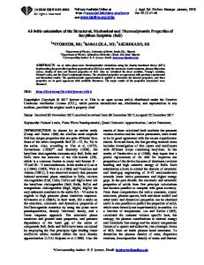
Interstitial Atoms. For interstitial atoms, direct experimental estimation of energy parameters is impossible, and therefore data on interstitial atoms in silicon can be obtained by simulation. It is currently believed that four stable interstitial atom configurations with different formation energies may exist in silicon. These include two natural interstitial configurations in which the interstitial silicon atom is located in tetrahedral (T) and hexagonal (H) interstitial positions and two dumbbell configurations formed by two silicon atoms oriented along the direction. These configurations are often referred to as split (X) and extended split (EX) configurations (see Figure).
Figure: Dumbbell Interstitial Atom Configurations in Silicon Crystal: (a) X and (b) EX. In Both Cases the Interstitial Pair (••) is Oriented Along the Direction
Table 6 presents interstitial atom formation energy calculation data for different interstitial atom types compared with ab initio calculation data of other researchers and with calculations made for the same configurations made using a number of widely used semiempirical interatomic potentials. Almost all the GGA data predict interstitial atom formation energy for the X configuration at 3.7–3.8 eV while LDA data typically yield 3.3–3.4 eV. For both approximations, the interstitial atom energy predictions are very close for the X and H configurations. For sufficiently large calculation cells the dumbbell configuration is preferable but the energy advantage is just several hundredths of eV. The interstitial atom energy for the tetrahedral position is 0.2–0.3 eV higher than for the split dumbbell. EX type interstitial atom formation energy estimates suggest that they are noticeably less energetically advantageous than even for the tetrahedral configuration. A similar qualitative result for LDA was referred to earlier [24] although the authors did not provide any numerical data. Table 6. Theoretical Formation Energies EfI (eV) for Different Types of Interstitial Atoms in Silicon Approximation or Potential
GGA
LDA
SW Tersoff EDIP MEAM
Number of Atoms in Cell 300 64 64 128 216 216 256 128 128 216 216 2400 2400 2400 2400
Interstitial Atom Type X
H
ab initio Methods 3.73 3.76 3.70 3.80 3.84 3.80 3.84 3.80 3.31 3.31 3.67 3.77 3.73 3.79 — — 3.31 3.31 2.87 2.87 3.42 3.42 Semiempirical Methods 4.40 4.41 4.35 4.63 3.38 4.05 3.34 n/a
Reference
T
EX
3.93 5.10 4.07 4.07 — 4.09 4.06 — 3.43 — 3.56
4.37 — — — — — — — — — —
— [24] [25] [26] [15] [27] [28] [26] [25] [15] [27]
4.92 3.69 4.16 3.655
3.66 3.84 3.5 4.14
— — — —
Calculations of the effect of 64 atom cell adjustment on the interstitial atom formation energy are summarized in Table 7 for the most energetically advantageous dumbbell configuration. The general trend shows that the GGA calculated energy is slightly higher than the LDA calculated one. Unlike vacancy defects, silicon atom incorporation into the silicon lattice causes its local dilatation and increases
the average lattice parameter. However, the interstitial atom formation energy advantage is less than 0.1 eV compared to the data shown in Table 6. Thus, the split interstitial atom configuration distorts the silicon lattice relatively weakly. Table 7. Theoretical Lattice Parameters aPMA and Formation Energies EfI for an X-Type Dumbbell Configuration in an Adjustable 64 Atom Cell Approximation GGA—PAW LDA—PAW
aI, nm 0.5491 0.5424
EfI, eV 3.67 3.31
We will now demonstrate the application of these results for the estimation of semiempirical interatomic potentials in the simulation of interstitial atom dynamics in silicon. As can be seen from Table 6, the two most widely used potentials for silicon (SW and Tersoff) are almost unsuitable for this purpose because they predict the main state of the interstitial atom incorrectly. The EDIP and MEAM potentials correctly predict the lowest energy configuration but incorrectly reproduce the energy sequence of metastable configurations. For example, neither of them predicts the proximity of the energies for the X and H configurations. Furthermore, the use of EDIP gives unjustified preference to the EX configuration instead of H. Thus, molecular dynamic simulation results for interstitial atom diffusion in silicon should be treated with care. Summary Comparison of the results for the effect of different ab initio calculation approximations on point defect formation energies in silicon demonstrated that the results depend are the most sensitive to the choice of the exchange correlation potential. The choice of the model for the description of valence electron interaction with inner shells of ions affects the prediction results but slightly. The choice between constant or adjustable calculation cell size affects the prediction result significantly only for small cells, whereas for 64 silicon atom cells this factor becomes secondary. We demonstrated a general trend showing that the GGA predicted silicon point defect formation energies are slightly higher than the LDA predicted ones. We also demonstrated for interstitial atoms in silicon how ab initio calculation results can be used for assessing the reliability of classical atomic simulation methods.
References 1. Pelaz L., Marques L.A., Aboy M., Lуpez P., Santos I. Front-end process modeling in silicon. Eur. Phys. J. B. 2009, vol. 72, pp. 323—359. 2. Kohn W., Sham L. J. Self-consistent equations including exchange and correlation effects. Phys. Rev. 1965, vol. 140, pp. A1133—A1138. 3. Perdew J.P., Chevary J.A., Vosko S.H., Jackson K. A., Pederson M. R., Singh D. J., Fiolhais C. Atoms, molecules, solids, and surfaces: Applications of the generalized gradient approximation for exchange and correlation. Phys. Rev. B. 1992, vol. 46, pp. 6671—6687. 4. Kresse G., Joubert D. From ultrasoft pseudopotentials to the projector augmented-wave method. Phys. Rev. B. 1999, vol. 59, pp. 1758—1775.
5. Vanderbilt D. Soft self-consistent pseudopotentials in a generalized eigenvalue formalism. Phys. Rev. B. 1990. vol. 41, pp. 7892—7895. 6. Probert M. I. J., Payne M. C. Improving the convergence of defect calculations in supercells: An ab initio study of the neutral silicon vacancy. Phys. Rev. B. 2003, vol. 67, p. 075204. 7. Corsetti F., Mostofi A. A. The silicon vacancy: insights from large-scale electronic structure calculations and maximally-localized Wannier functions. Phys. Rev. B. 2011, vol. 84, p. 035209. 8. Stillinger F. H., Weber T. A. Computer simulation of local order in condensed phases of silicon. Phys. Rev. B. 1985, vol. 31, pp. 5262—5271. 9. Tersoff J. Modeling solid-state chemistry: interatomic potentials for multicomponent systems. Phys. Rev. B. 1989, vol. 39, pp. 5566—5568. 10. Justo J. F., Bazant M. Z., Kaxiras E., Bulatov V. V., Yip S. Interatomic potential for silicon defects and disordered phases. Phys. Rev. B. 1998, vol. 58, pp. 2539—2550. 11. Jelinek B., Groh S., Horstemeyer M. F., Houze J., Kim S. G., Wagner G. J., Moitra A., Baskes M. I. Modified embedded atom method potential for Al, Si, Mg, Cu, and Fe alloys. Phys. Rev. B. 2012, vol. 85, p. 245102. 12. Puska M. J., Poykko S., Pesola M., Nieminen R. M. Convergence of supercell calculations for point defects in semiconductors: vacancy in silicon. Phys. Rev. B. 1998, vol. 58, pp. 1318—1325. 13. Dannefaer S., Mascher P., Kerr D. Monovacancy Formation Enthalpy in Silicon. Phys. Rev. Lett. 1986, vol. 56, pp. 2195—2198. 14. Watkins G. D. Defects and Their Structure in Non-metallic Solids. NY: Plenum, 1976. 15. Goedecker S., Deutsch T., Billard L. A Fourfold Coordinated Point Defect in Silicon. Phys. Rev. Lett. 2002, vol. 88, p. 235501. 16. Wright A. F. Density-functional-theory calculations for the silicon vacancy. Phys. Rev. B. 2006, vol. 74, p. 165116. 17. Al-Mushadani O. K., Needs R. J. Free-energy calculations of intrinsic point defects in silicon. Phys. Rev. B. 2003, vol. 68, p. 235205. 18. Watkins G. D., Corbett J. W. Defects in Irradiated Silicon: Electron Paramagnetic Resonance of the Divacancy. Phys. Rev. 1965, vol. 138, pp. A543—A555. 19. Pellegrino P., Lévêque P., Lalita J., Hallén A., Jagadish C., Svensson B. G. Annealing kinetics of vacancy-related defects in low-dose MeV self-ion-implanted n-type silicon. Phys. Rev. B. 2001, vol. 64, p. 195211. 20. Song E., Kim E. G., Lee Y. H., Hwang Y. G. Fully relaxed point defects in crystalline silicon. Phys. Rev. B. 1993, vol. 48. pp. 1486—1489. 21. Pesola M., von Boehm J., Pöykkö S., Nieminen R. M. Spin-density study of the silicon divacancy. Phys. Rev. B. 1998, vol. 58, pp. 1106—1109. 22. Staab T. E. M., Sieck A., Haugk M., Puska M. J., Frauenheim Th., Leipner H. S. Stability of large vacancy clusters in silicon. Phys. Rev. B. 2002, vol. 65, p. 115210.
23. Svensson B. G., Johnsson K., Xu D. X., Svensson J. H., Lindstrom J. L. Annealing of divacancyrelated infrared absorption bandin boron-doped silicon. Radiat. Eff. Def. Sol. 1989, vol. 111, pp. 439— 447. 24. Tang M., Colombo L., Zhu J., de la Rubia T. D. Intrinsic point defects in crystalline silicon: Tightbinding molecular dynamics studiesof self-diffusion, interstitial-vacancy recombination, and formation volumes. Phys. Rev. B. 1997, vol. 55, pp. 14279—14289. 25. Leung W.-K., Needs R. J., Rajagopal G., Itoh S., Ihara S. Calculations of Silicon Self-Interstitial Defects. Phys. Rev. Lett. 1999, vol. 83, pp. 2351—2354. 26. Needs R. J. First-principles calculations of self-interstitial defect structures and diffusion paths in silicon. J. Phys.: Condens. Matter. 1999, vol. 11, pp. 10437—10450. 27. Mattsson A. E., Wixom R. R., Armiento R. Electronic surface error in the Si interstitial formation energy. Phys. Rev. B. 2008, vol. 77, p. 155211. 28. Centoni S. A., Sadigh B., Gilmer G. H., Lenosky T. J., de la Rubia T. D., Musgrave Ch. B. Firstprinciples calculation of intrinsic defect formation volumes in silicon. Phys. Rev. B. 2005, vol. 72, p. 195206.
Acknowledgements. The article was written based on an interdisciplinary scientific and practical seminar «Mathematical Modeling in Materials electronic nanostructures», held in the Institution of Russian Academy of Sciences Dorodnicyn Computing Centre of RAS.
Mariya Gerasimovna Ganchenkova1 — Сand. Sci. (Phys.Math.), Senior Researcher (
[email protected]); Irina Anatolevna Supriadkina 2 — Graduate Student the Faculty of Physics, Moscow State University, Research Associate at the Dorodnitsyn Computing Center of RAN (
[email protected]); Karine Karlenovna Abgaryan3 — Сand. Sci. (Phys.Math.), Head of the Section (
[email protected]); Dmitriy Igorevich Bazhanov 4 — Сand. Sci. (Phys.Math.) (dmibaz@sols3475.phys.msu.ru); Ilya Vasylovich Mutigullin 3 — Сand. Sci. (Phys.Math.), Senior Researcher (
[email protected]); Vladimir Alekseevich Borodin 2 — Dr. Sci. (Phys.Math.), Leading Researcher.
Fig. 1