Input common-mode adapter using multiple-input floating-gate devices Y.-S. Kim, K.-S. Sohn, K.-J. Baek, N.-S. Kim, S.F. Al-Sarawi and D. Abbott A new common-mode (CM) feedback circuit for differential amplifiers that uses floating-gate devices is demonstrated. The circuit, which consists of a floating-gate CM voltage detector and a two-stage amplifier, generates a CM correction voltage to stabilise the floating-gate voltage of a differential amplifier against the input CM voltage. The proposed method achieves a rail-to-rail CM swing and a transconductance that is independent of the input CM voltage.
Introduction: Basic building blocks of analogue ICs include the operational amplifier (opamp) and the operational transconductance amplifier (OTA). The differential input pair used in opamps and OTAs has an inherent limitation of reduced input common-mode range (CMR) [1]. This problem can be avoided with parallel-connected complementary differential pairs in the input stage [2], but this method sets a minimum requirement on the supply voltage, limiting its application to supply voltages in the order of 3 V. In addition, this technique results in a varying opamp transconductance depending on the input common-mode (CM) voltage, and therefore extra circuits are necessary to keep the transconductance constant [3]. There are several other techniques to obtain a rail-to-rail input CM swing. A floating-gate MOSFET differential pair was proposed in [4], but its transconductance changes as a function of the input CM voltage. Another technique is the use of a resistive dynamic level shift, which adapts the input CM voltage based on a CM feedback loop [5]. In this Letter we propose a differential amplifier with an input CM adapter circuit using floating-gate devices. The negative CM feedback circuit stabilises the floating-gate voltage of the differential input amplifier when the input CM voltage changes. Therefore, our proposed method herein achieves not only a rail-to-rail CM swing, but also constant transconductance when the input CM voltage changes.
M12
M15
M3 M8
Cin Vin–
M11
M10 CCM
CCM
Cin Vin+ M16
Vin–
M1 CCM
M2
Cin
CCM
Vin+ IL
VCMAD
R M13 M18 Vss
M9
Cin
M14 M17
common-mode adapter
M6
M4 M5
Measurement results: The OTA with the proposed CM adapter was realised using commercially available inverter arrays (HCF4007UB). This chip comprises three n-channel and three p-channel enhancement type MOS transistors. In the measurements, the supply voltage VDD was 6 V (VSS ¼ 0 V) and the drain current of each transistor was 100 mA. Capacitors Cin and CCM were sufficiently large to avoid any charging or discharging through the ESD diodes of inverter arrays (470 and 680 pF, respectively, were used in our measurements). When the proposed CM circuit is realised into an integrated circuit environment, the size of these capacitors can be significantly reduced. Measured total drain currents of the differential input pair of the OTA with and without the CM adapter are shown in Fig. 2. The total drain current of the differential input pair without the CM adapter decreases when the input CM voltage increases from 0.5 to 4 V. This is because the drain voltage of current source M3 for the differential input pair increases so that source-drain voltage, and therefore the drain current of M3, decrease when VCM increases. If we further increase VCM , total drain current decreases to zero. This is because, when VCM increases to more than 4 V, transistor M3 is no longer in the saturation region and the source-drain voltage of M3 decreases to zero. On the other hand, when using the input CM adapter, the drain current of the differential input pair of the OTA is constant. When VCM increases, the floating-gate voltage of the differential input pair increases also by the capacitive coupling of the input CM voltage through Cin , but the input CM correction signal VCMAD decreases to compensate for this increased floating-gate voltage. Therefore, the floating gate CM voltage of the input pair of the OTA should remain substantially constant owing to the correction loop, so as to keep the total drain current in the differential pair constant.
M7
300
OTA
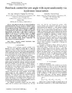
Fig. 1 Circuit diagram of OTA with proposed CM adapter using floatinggate devices Floating-gate devices
Proposed circuit: A CMOS OTA with the proposed CM adapter using a multiple-input floating-gate differential input pair is shown in Fig. 1. The main differential pair of the OTA consists of floating-gate devices where the CM correction signal VCMAD is applied through the capacitors CCM. The CM adapter consists of a CM detector using a multiple-input floating-gate differential pair identical to that of the main OTA and twostage amplifier in which output is fed back to the floating-gate of the input transistors of the CM adapter. The input CM signal level is detected by connecting the drain terminals of differential transistors M10 and M11, while at the same time the differential input signals are eliminated at this node. The gain of the CM detector stage is given by 22 × gm10/gm13. The detected CM level is further amplified by common-source amplifiers M14– M15 and M16– M17 to provide enough loop gain for the negative feedback system. The frequency compensation of the CM adapter can be accomplished through CCM and Cin. The operation of the input CM adapter is as follows. Suppose that the input CM voltage is higher than the nominal CM value, commonly defined by half supply voltage. A higher input CM signal level results in a reduction in the drain voltages of M10 and M11, which are lowered further by the common-source amplifiers M14– M15 and M16– M17. This CM correction signal, VCMAD , is then applied to the floating-gate of the differential pair in the CM adapter through the capacitors CCM. Therefore, VCMAD decreases the floating-gate voltage
total drain current, mA
VDD M19
which counteracts the floating-gate voltage increase by the higher input CM signal. As a result, the CM drain currents of the differential pair in the CM adapter stay fixed regardless of any variation in the input CM voltage. The input CM correction signal VCMAD is now applied to the differential input pair in the OTA through CCM capacitors and thus calibrates the varying input CM signal of the OTA. The CM drain currents of the differential input pair of the OTA are now constant and do not vary as a function of the input CM signal. Furthermore, the transconductance of the OTA is constant though the input CM signal might be varied. Note that CM drain currents of the differential input pair of the conventional OTA without the CM adapter decrease as the input CM signal increases and when VCM . VDD − Vdsat(M3) − Vdsat(M1) − |VTHp |, the differential input pair M1 and M2 ceases to pass current.
200
100 without CM adapter with CM adapter
0 0
1
2
3
4
5
6
input CM voltage, V
Fig. 2 Measured total drain current of differential input pair M1 and M2 with and without proposed CM adapter against input CM voltage Note that Cin ¼ 470 pF and CCM ¼ 680 pF
Measured OTA transconductances with and without the CM adapter, and with a 1 kV load resistor, are shown in Fig. 3. As can be seen from these measurements, the transconductance of a conventional OTA without the CM adapter decreases significantly after VCM . 4 V, because M3 is no longer operating in the saturation region. On the other hand, the transconductance of the OTA with the proposed CM adapter is maintained at a constant level when the input CM voltage changes from 0.5 to 5.5 V. The transconductance of the OTA with the proposed CM adapter drops to 41% of that of the conventional OTA without the CM adapter. This reduction is due to input capacitor coupling loss through Cin. The transconductance of the OTA with the CM adapter can be increased by increasing the ratio of Cin to CCM. However, care should be taken to ensure that the VCMAD is kept
ELECTRONICS LETTERS 16th September 2010 Vol. 46 No. 19
within Vdsat(M17) and VDD 2 Vdsat(M16) , to prevent both transistors M16 and M17 moving into the triode region. Note that both transconductances with and without the input CM adapter have same value at VCM ≃ 4.6 V as shown in Fig. 3, however drain currents with and without the input CM adapter have same value at VCM ≃ 3.5 V in Fig. 2. This is because the transconductance with the input CM adapter in Fig. 3 is an effective value. In presented implementations of the CM adapter, the used components, such as MOSFETs and capacitors, were unmatched, so the offset voltage of the OTA could not be controlled. However, in the context of an integrated circuit environment, the offset issue can be solved with commonly used component matching techniques. Also note that any charge in the floating nodes injected during the fabrication process causes the offset voltage and can be removed using UV erasure or other techniques.
Acknowledgment: This work was supported by a grant from the Korean Ministry of Education, Science and Technology (The Regional Core Research Program/Chungbuk BIT Research-Oriented University Consortium). # The Institution of Engineering and Technology 2010 29 June 2010 doi: 10.1049/el.2010.1775
500
Y.-S. Kim, K.-S. Sohn, K.-J. Baek and N.-S. Kim (Department of Semiconductor Engineering, Chungbuk National University, Cheongju, Chungbuk, 361-763, Republic of Korea)
400
E-mail:
[email protected]
300
S.F. Al-Sarawi and D. Abbott (School of Electrical and Electronic Engineering, University of Adelaide, SA 5005, Australia)
600
gm, mS
the use of discrete componentry, and thus represents a worst-case upon which future IC implementation can further enhance performance. The proposed OTA with the CM adapter can be used in analogue applications such as biomedical sensors where the input CM voltage is not controlled.
200
References
without CM adapter with CM adapter
100 0 0
1
2 3 4 input CM voltage, V
5
6
Fig. 3 Measured transconductance of OTA with and without input CM adapter against input CM voltage. Note that Cin ¼ 470 pF and CCM ¼ 680 pF
Conclusion: A differential amplifier with a new CM adapter, using a floating-gate technique, has been proposed and realised in an OTA using commercially available inverter arrays. Measurement results verified that the proposed CM circuit maintained a constant bias current for the differential input amplifier of the OTA regardless of the input CM voltage variation. The experimental performance was achieved despite
1 Baker, R.J.: ‘CMOS: circuit design, layout, and simulation’ (Wiley-IEEE Press, New Jersey, 2007) 2 Steyaert, M., and Sansen, W.: ‘A high-dynamic-range CMOS op amp with low-distortion output structure’, IEEE J. Solid-State Circuits, 1987, SC-22, (6), pp. 1204–1207 3 Coban, L., Allen, P.E., and Shi, X.: ‘Low-voltage analog IC design in CMOS technology’, IEEE Trans. Circuits Syst. I, 1995, 42, (11), pp. 955– 958 4 Ramirez-Angulo, J., Urquidi, C.A., Gonzalez-Carvajal, R., Torralba, A., and Lopez-Martin, A.: ‘A new family of very low-voltage analog circuits based on quasi-floating-gate transistors’, IEEE Trans. Circuits Syst. II, 2003, 50, (5), pp. 214– 220 5 Baez-Villegas, D., Silva-Martinez, J.: ‘Quasi rail-to-rail very low-voltage OPAMP with a single pMOS input differential pair’, IEEE Trans. Circuits Syst. II, 2006, 53, (11), pp. 1175– 1179
ELECTRONICS LETTERS 16th September 2010 Vol. 46 No. 19