Integrated Heterodyne Array Receivers for Submillimeter Astronomy
C.K. Walkera*, C.E. Groppia , C. Drouet d’Aubignya, C. Kulesaa, A. Heddena, D. Proberb, I. Siddiqib, J. Kooic, G Chend , A.W. Lichtenbergere a)Steward Observatory, University of Arizona; b)Yale University, c)California Institute of Technology; d) NASA Goddard Spaceflight Center, e) University of Virginia ABSTRACT The advent of large format (~100 pixels) spectroscopic imaging cameras at submillimeter wavelengths would fundamentally change the way in which astronomy is performed in this important wavelength regime. While the possibility of such instruments has been discussed for more than two decades1, only recently have advances in mixer technology, device fabrication, micromachining, digital signal processing, and telescope design made the construction of such an instrument possible and economical. In our paper, we will present the design concept for a 10x10 heterodyne camera. Keywords: SIS Heterodyne Array Receiver Submillimeter Molecular Spectroscopy
1.Motivation In the wavelength regime between 300 and 60 microns there are a number of atomic and molecular emission lines that are key diagnostic probes of the interstellar medium. These include transitions of CII, NII, OI, HD, OH, CO, and H2O. In Giant Molecular Clouds (GMCs), evolved star envelopes, and planetary nebulae, these emission lines can be extended over many arc minutes and possess complicated line profiles that can only be disentangled using high resolution (R>106) spectroscopy. Observations of these lines are crucial to understanding the chemistry and energy balance of the ISM. It is the cooling provided by these lines that governs the star formation process and traces the formation of molecules in evolved stars that ultimately replenishes the ISM. Due to the hot (T>1000K) and dense (nH2 > 1012) conditions expected in many Figure 1: An overview of first generation protoplanetary disks, emission lines in the FIR will also SOFIA instruments, plotting spectral resolving play a pivotal role in cooling and molding young planetary power versus mapping speed, here measured by systems. In order to separate the emission of the disks the number of spatial pixels. No instrument is from that of the ever present molecular outflows and probe capable of widefield mapping at high spectral velocity fields, instruments incorporating both high resolution. spectral resolution and imaging capabilities are again required. The only instruments capable of realistically providing the high spectral resolution needed for these studies are heterodyne receivers. Fortunately, recent breakthroughs in detector technology, micromachining, local oscillators, amplifier technology, and backend spectrometers now make the construction of large arrays of heterodyne receivers possible. In this paper we will provide a brief description of one way in which a large (10x10), superconducting heterodyne camera (SuperCAM) can be assembled. Given the venue of this conference, we will cast the array in the form of an instrument for the Antarctic Submillimeter Telescope & Remote Observatory (AST/RO), although the same technology *
[email protected]; phone 520-621-8783; fax 520-621-1532; http://soral.as.arizona.edu; Steward Observatory, 933 N. Cherry Ave, Tucson, AZ, USA 85721
can be used to build arrays for SOFIA, balloon, or space based platforms. For example, Figure 1 compares the capabilities of SOFIA's first light instruments in terms of number of pixels versus spectral resolution. When viewed in this way, there is a clear, urgent need for SuperCAM type instruments. Projections of the 1.5 THz beam footprint of a 10x10 SuperCAM AST/RO instrument on Eta Carina is shown in Figure 2.
2.Instrument Concept 2.1.
Introduction
Submillimeter heterodyne receivers have advanced dramatically in the past decade, and these advances will be incorporated, and further developed, in new missions such as SOFIA and Herschel/FIRST. Up to 1 THz, almost all (cryogenic) receivers use niobium (Nb) based SIS mixers. SIS mixers will likely be Figure 2: The array footprint of SuperCAM used to 1.2 THz in the future, with a likely upper limit of about at 1.5 THz on the AST/RO telescope, 1.4 THz due to film losses and junction gap frequency for known overlaid on Eta Carina. Each circle film materials and devices. The required LO power is of order 1 represents one diffraction limited beam mW. Below 0.7 THz, the receiver noise (DSB) is approximately (FWHM). (2 to 4) x TQ with TQ =hf/kB = 48K x f(THz) (e.g. TQ = 40 K at 0.8 THz). Above 0.8 THz, the noise rises to a larger value than this formula, due to losses in the film circuit used to resonate out the SIS junction capacitance. Schottky mixers are presently employed at frequencies above 1 THz2. Hot Electron Bolometer (HEB) mixers with much lower noise and PLO are now ready for use in this higher frequency range3. An HEB device utilizes 10-100 times less LO power, requires no magnetic field, and has a much broader bandwidth. These characteristics make HEBs an excellent choice for THz focal plane arrays.
2.2.
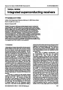
Figure 3a: SEM image of a portion of a 1x10 array of 5 THz Potter horns, with a full phase retrieval hologram of the throat of one horn. Figure 3b: SEM image of a portion of a 1x5 array of 1.5 THz corrugated feedhorns, and a close-up SEM image of a single horn.
Micromachined Waveguide Mounts
HEBs have been successfully used in both quasioptical and waveguide mixer mounts. When waveguide and quasi- optical mixers are made at the same frequency with comparable mixing devices, laboratory measurements show waveguide mixers outperform quasi-optical mixers both electrically and optically4. This occurs because waveguide has an intrinsically lower loss than the microstrip structures used in planar designs and waveguide feedhorns can couple to the fundamental Gaussian mode with a ~98% efficiency, compared to the ≤89% efficiency of dielectric lens-planar antennas5. We have used a new laser milling technique to fabricate high quality, THz waveguide components and feedhorns. Once metallized, the structures have the properties of standard waveguide components6. We have recently used this technology to fabricate 1x5 arrays of corrugated feedhorns and 1x10 arrays of dual-mode (Potter) horns for designed for operation at 1.5 THz (200 microns) and 5 THz (60 microns) respectively.
Electron microscope and optical photographs of these structures are shown in Figures 3a and 3b.It took only a matter of minutes to fabricate the 5 THz array and ~2 hours to make the 1.5 THz array.
2.3.
Focal Plane Array Concept
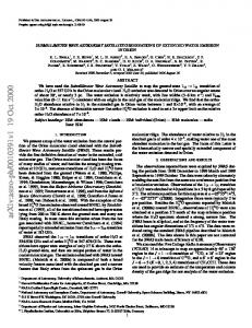
All waveguide components for the arrays can be micromachined out of silicon and assembled into an integrated package. The array design and fabrication can be readily scaled for use from 1 to 5 THz. A conceptual design for a 4x4 array of micromachined fixed-backshort, waveguide mixers is shown in Figure 4. The focal plane array consists of a "Horn Block", "Bolometer Block" and "Backshort Block". In this example, the Horn Block consists of four, 1x4 corrugated feedhorn subarrays. Each subarray is formed by bonding two gold plated, silicon wafers in which mirror images of the corrugated feedhorns have been laser micromachined. Assembly of the package can be done with the aid of an infrared microscope and micromanipulator system designed originally for flip-chip bonding. Each horn is micromachined with a circular-to-rectangular waveguide transition (see Fig. 3a) to match the input impedance of the HEB. At high frequencies (650 GHz) it becomes nearly impossible to manually mount detectors across small waveguide structures. Figures 4 & 5: An assembly drawing of a 4x4 An alternative approach is to fabricate the mixing micromachined mixer mount, and a cutaway drawing elements on ~1 micron thick silicon nitride of a single pixel detailing the three primary membranes which subsequently are integrated with components. the horn structure. An exploded view of an individual mixer block is shown in Figure 5. In the array, we adopt this approach and use a suspended stripline RF choke design similar to that of Blundell & Tong7. We also micromachine a novel RF choke structure8 at the horn and bolometer block interface. These chokes help relax the mechanical tolerances between the pieces. The choke and waveguide probe designs were optimized using Hewlett Packard's High Frequency Structure Simulator (HFSS). The impedance of an HEB (~50 Ohm) is mostly resistive and does not vary significantly with frequency. This property allowed us to design a very broadband waveguide probe for use with HEBs. The widest bandwidth was achieved using an asymmetric probe similar in principle to that described by Kerr et al9. HFSS calculations indicate the mixer will have an operational bandwidth >45%! (A more detailed discussion of this style of waveguide probe can be found in Kooi et al., this volume.) The separation between mixers in the instrument focal plane is approximately given by ~2fλ (e.g. ~3.6 mm at 1.5 THz on AST/RO and ~2.4 mm at 5 THz on SOFIA). Since all the mixers share a common Bolometer Block, crosstalk between array pixels could be a concern. Using HFSS, we have carefully constructed a 2x2 simulation of an array with only ~1 mm separation and found the crosstalk to be down below the -35 dB level across the band. The IF output of each mixer is ultimately conveyed to wire bonding pads on the periphery of the bolometer block by microstrip lines.
2.4.
Local Oscillator and IF Processing
Unlike the situation often encountered in conventional single pixel and array receivers, for an integrated array like the one discussed here, it is the choice of the Intermediate Frequency (IF) center frequency and bandwidth that determines
the size and cost of the array camera. In the integrated design the waveguide mixers are micromachined out of silicon using computer controlled laser micromachining and wet etching techniques. With this approach it costs the same to make ~10 mixers as to make just one. In both SIS and HEBs fabrication runs, typically 100's of devices are made at once on a single wafer. Our concept of having a single, common bolometer block or wafer does not add significantly to the cost or complexity of device fabrication. Since HEBs require ~30 times less LO power than SIS devices, a commercially available FIR laser system can easily drive the entire array. Within a few years solid state frequency multipliers are expected to achieve output powers that will make them viable alternatives as LO sources for THz arrays. Indeed, at frequencies below ~810 GHz, existing solid-state sources can generate output power in excess of 1 mW, more than sufficient for pumping large arrays of SIS devices (see discussion of frequency multipliers by Mehdi, this volume). The additional cost per pixel is driven by the cost of the IF components and the spectrometer needed to process the signal. Fortunately these costs are also dropping. For heterodyning the astrophysically important NII, H2D+, and CO 1110 lines in the 200 micron (1.5 THz) atmospheric window, strong laser lines yielding IF frequencies of 4.6 GHz, 7.64 GHz, and 5.2 GHz are available10. IF frequencies up to 9 GHz have been demonstrated to yield low noise response in both phonon and diffusion-cooled HEBs11, 12. Fortunately, MIMIC HEMT amplifier devices are now becoming available that have noise, gain, and power specifications over a 10 GHz bandwidth that make them essentially ideal as 1st stage IF amplifiers for array applications.
Figure 6: The SuperCAM 3He cryostat, showing the “array motherboard” packaging concept.
Traditionally, when designing submillimeter-wave receiver systems for astronomy, one strives to provide the user with as wide a spectrometer bandwidth as possible (several GHz). Such wide bandwidths are extremely useful for spectral line surveys and protogalaxy searches. However, for many galactic astronomy projects, the user is targeting a single, relatively narrow (≤10 km/s) line. In star formation regions, these lines are often extended over many beamwidths. Under these fairly common conditions, it is more profitable to trade `bandwidth for pixels'. For example, at 1.5 THz, 100 km/s of velocity coverage corresponds to only 500 MHz of IF bandwidth. At 5 THz, 1.7 GHz of bandwidth is needed to obtain this velocity coverage. Velocity resolutions of ~1 km/s over these velocity ranges can be obtained relatively easily using available correlator chips. Indeed, within the next year, correlator chips with 2.5 GHz bandwidth, and 128 lags will become available13. With such chip sets, 2-bit/4-level correlator systems capable of supporting 100 pixel arrays can be built that fit into two VX Works type crates.
2.5.
Array Motherboard
Running bias wires and cabling to even a small number of mixers can be an arduous task. Bias wires are required for the mixing device and IF amplifier. Coaxial cable must be used between the mixer, 1st IF amplifier and the outside world. Since the mixer is typically at or below 4 K, the IF amplifier at ~15 K, and the outside world is at 290 K, the materials from which the cables are made and how they are heat strapped are critical to the cryogenic performance of the system. Since our goal is to develop the techniques for making large format arrays, we must use a different approach. Fiberglass standoffs are often used to thermally-isolate one stage of a cryostat from another. Fiberglass is also commonly used in printed circuit boards. We propose to combine these two functions and make a PC `motherboard' for conveying bias and IF signals into and out of the focal plane array. A conceptual design for the motherboard is shown in Figure 6. It is composed of a small (1.5 x 1.5 cm) `hub' surrounded by a series of nested frames. Each frame operates at a temperature
appropriate for the devices it carries. In the case of the Nb HEB arrays, the central hub containing the array and first stage IF amplifiers is at 4 K. The next frame out is at 60 K and contains the 2nd stage IF amps. The outer frame is at 290 K and contains the PC board mounted SMA cable jacks. Signals between the hub and frames are carried on thin dielectric strips. We have used Agilent’s Advanced Design System (ADS) software package to optimize the design of the microstrip and DC lines on the connecting strips. These lines are very thin (~3 mils wide) and are expected to have a very low thermal conductivity. Assuming each interconnecting strip carries 4 lines, the strips themselves need only be a few millimeters wide to insure crosstalk between the lines is at or below the -30 dB level. The thin, interconnecting strips will be designed with enough flexibility to tolerate the differential contraction between the frames. For the later operation with T < 1 K on the array stage, Nb or NbTi thin-film lines will couple from 4 K to 1 K to reduce the heat loading but provide high electrical conductivity.
2.6.
Array Cryostat
The Array Cryostat must be large enough to contain the array motherboard and provide the proper operating temperatures to each frame. For AST/RO, the holdtime of the cryostat should be ~24 hours, preferably 2-3 days. One cryostat design (all liquid) that would meet these requirements is shown in Figure 6. It uses a He-3 stage to cool the HEBs to ~300mK. The cryostat is only 25" in diameter and 24" high. An alternative cryogenic technology that can provide closed-cycle, low-vibration cooling to ~4 K are pulse tube refrigerators14. These coolers can provide in excess of 1 watt of thermal capacity at 4K and are reliable and essentially maintenance free.
2.7.
Optics
In Figure 7 we show the optical design for realizing a 10x10 pixel heterodyne array on AST/RO. The array cryostat is mounted on the Nasmyth focus because of the greater field of view it provides. From the warm receiver room (located just below the telescope) optical constraints limit the size of the array to 3x3. The instrument will be completely enclosed in a housing that will keep it at a suitable operating temperature. The telescope beam first reflects off a secondary and tertiary mirror before it passes through a silicon beam splitter. The beam splitter injects the local oscillator beam from the FIR laser (located in the warm receiver room) into the focal plane array15. The FIR laser beam is efficiently divided into 100, equal power beams by reflecting off a custom designed phase grating (see discussion of phase gratings by Graf et al. this volume). The horns in the array are spaced to provide adequate coverage of the focal plane. Only a dielectric lens is required to make the final match between the telescope beams and the array feedhorns.
Figure 7: A diagram showing the integration of SuperCAM with the AST/RO telescope optics. The instrument is at the Nasmyth focus, while the LO is located in the receiver room and is directed back towards the instrument via a holographic phase grating.
3.Summary Technological advances now make it possible to consider the construction of large-format, integrated arrays at THz frequencies. Such arrays would be more than two orders of magnitude faster than current receivers when imaging large areas. We estimate the cost per pixel to be ~20 times less than typical single channel systems. The advent of large format heterodyne arrays in the FIR would have a dramatic impact on how high resolution spectroscopy is done in this important wavelength regime. We describe how a 10x10 focal plane array can be implemented on AST/RO.
BIBLIOGRAPHY 1. 2. 3. 4. 5. 6. 7. 8. 9. 10. 11. 12. 13. 14. 15.
Gillespie, A.R. & Philips, T.G. 1979, A&A,73-1,14. Gaidis, M. et. al. 2000, IEEE MTT, 48, 733. Karasik, B.S. 1999, Appl. Phys. Let. 68, 853. Kooi, J. et. al. 1998, IEEE MTT, 46, 151. Goldsmith, P. 1998, "Quasioptical Systems," pub. IEEE press, 184. Walker, C. et al. 1998, Proc. SPIE, 3357, 45. Blundell, R. & Tong, C-Y. E., 1995, IEEE MTT, 43, 933. Hesler, J. 2001, Microwave Symposium Digest, IEEE MTT-S International, 2, 151. Kerr, A. et. al. 1992, IEEE Microwave and Guided Wave Letters, 2-11, 454. Boreiko, R. T. & Betz, A. L., 1993, Ap. J (Letters), 405, L39. Yngvesson, S., Private communication, 2002. McGrath, R. et al., 1999, Proc. SPIE, 3617, 80. Timoc, C., Private communication, 2002. Kittel, P., Private communication, 2002. Mueller E., Private communication, 2002.