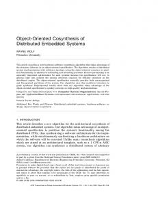
workstation or a laptop all the way to simple identification tags for tracking people and ...... lenged with meeting performance constraints while mini- mizing cost.
Interface CO-Synthesis Techniques for Embedded Systems * Pai Chou, Ross B. Ortega, Gaetano Borriello Department of Computer Science & Engineering, Box 352350 University of Washington, Seattle, WA 98 195-2350 {chou,ortega,gaetano}@cs.washington.edu Abstract A key aspect of the synthesis of embedded systems is the automatic integration of system components. This entails the derivation of both the hardware and sofrware intefaces that will bind these elements together and permit them to communicate correctly and efficiently. Without the automatic synthesis of these intefaces, designers are not able to fully simulate and evaluate their systems. Frequently, they are discouragedfrom exploring the design space of different hardwarehoftware partitions because practical concerns mandate minimizing changes late in the design cycle, thus leading to more costly implementations than necessary. This paper presents a set of techniques that form the basis of a comprehensive solution to the synthesis of hardwarehoftware inte$aces. Software drivers and glue logic are generated to connect processors to peripheral devices, hardware co-processors, or communication interfaces while meeting bandwidth and peijomuznce requirements. We use as examples a set of devices that communicate over an infrared local communications network (highlighting a video wrist-watch display) to explain our techniques and the need for design space exploration tools for embedded systems.
transceiver for a laptop can use more expensive components that support more robust and efficient communication. To help identify the possible optimizations, consider the video wrist-watch system shown in Fig. 1. It has a grayscale video camera whose images are scaled to the size of the wrist-watch display (128x128 8-bit pixels), compressed using pixel and frame differencing techniques, and then transmitted over the omni-directional infrared link. The images are received at the wrist-watch, decompressed, and rendered on a small LCD screen. These pieces have a wide range of implementation choices. For example, either the decompression algorithm or the display controller could be implemented in custom hardware, or on the microprocessor that will also be handling the reception of IR packets. On the camera end, the camera controller, scaler, and compressor could also be in hardware, software, or a combination depending on the capabilities of the components used. To decide on the lowest cost mix of components and feasibility, designers must iteratively map the device's functionality to a particular hardwarehoftware partition and target architecture (i.e., the processors and devices to be used). Every time the designer explores a different system architecture, the interfaces must be redesigned. For instance, changing from a 16-bit processor to a 32-bit processor requires new glue logic and new device drivers. Altematively, a slower processor may require additional interface logic to meet the timing constraints of a fast peripheral device. Interfacing components requires managing many details in both hardware and software; however, no CAD tools are currently available to help designers with these interfacing issues. This is unfortunate as managing all of these details is so time consuming that designers typically cannot afford to evaluate many different implementations. The tendency is to make incremental changes that keep interfaces and device drivers fixed. This leads to overdesign, that is, the building in of extra capacity to handle unforeseen design changes, thereby increasing the cost. Automating the interface generation and system integration tasks is a critical part of the development of embedded system synthesis tools. Designers are quite capable of considering different global partitionings of their designs but need help in evaluating them. Interfacing and integrating system components are not only highly cumbersome and error-prone processes but also must be performed repeatedly. A tool that can manage these details and demonstrate the efficacy of the partition on a particular target architecture is critical to enabling a more complete exploration of
1 Introduction Designers of task-specific systems must deal with a wide collection of interfaces. Applications range from medical instrumentation to communication and networking devices to controllers in automobiles. There are many optimization opportunities because these systems have narrower and more specialized operational requirements, and users place fewer restrictions on the components that constitute the system. Optimizing the designs leads to an emphasis on design space exploration and system integration. Designers need to rapidly evaluate implementation options, that is, they must consider different partitionings and mixes of components. The most common activity in this type of exploration is integration of the components, i.e., generating the interfaces between them. As an example, consider the class of devices that can be used with an infrared local-area network [lo]. The types of possible devices range from transceivers connected to a workstation or a laptop all the way to simple identification tags for tracking people and objects. Each device must implement the same communication protocol but within very different cost constraints. For instance, identification tags must be small and inexpensive while a PC-Card (PCMCIA) 'This work was supported by ARPA DAAH04-94-G-0272
1063-6757195$04.00 0 1995 IEEE
280
--+ IR recv
addr db
decomp
cs wr
Fig. 1: The infrared video-wristwatch system. The camera unit transmits compressed video packets to a wrist-watch display.
Fig. 2: SCSI controller along with access waveform and corresponding SEQ.
the design space. This paper presents various techniques for the synthesis of the interface between hardware and software components in embedded systems. Section 2 describes the representation and main algorithm for synthesizing the interface using the processor's I/O resources (I/O ports and memory bus). Sections 3 and 4 describe the allocation of I/O ports and addresddata ports for performing direct YO. These techniques will introduce all of the necessary glue logic and generate device driver software. Section 5 describes the synthesis of the U 0 sequencers (FSMs) for cases where direct I/O cannot meet the performance requirements of the device. The sequencer itself is in turn interfaced as any other device.
After glue logic and partitioning decisions have been finalized, the device-drivers must be updated to reflect the binding of U 0 resources and the introduction of the interface hardware. In this section, we describe the representation and the algorithm for interface synthesis. 2.1 Representation The designer writes a high-level specification describing the behavior and lists the processors and peripheral devices used to implement the system. The input to the algorithm consists of descriptions for the processors, peripheral devices, and computations (in the form of control flow graphs). The first two are stored in the processor and device libraries, while the latter is derived from the behavioral description.
2 Hardwardsoftware Interface Synthesis The main goal in hardwarehoftware interface synthesis is to generate a communication link using minimal glue logic while respecting timing constraints. Automating the hardware/software interface allows designers to focus on higher-level decisions. To accomplish this requires developing the appropriate abstractions for device interfaces so that device drivers can be generated automatically. The description of the interface requirements must include detailed timing and bandwidth information for the tool to determine how the interface should be generated. The I/O capabilities of processors must also be specified in a general form. These include directly manipulable 1/0pins, interrupt mechanisms, and system bus interfaces. Given the two sides of the interface (device and processor), the tool should then be able to determine the best way to interconnect them and generate the corresponding interface software and hardware. The processor may use either direct I/O or indirect I.0. Direct U 0 manipulates the interface directly without glue logic, resulting in minimum hardware cost. Indirect U 0 means the processor communicates with the devices via auxiliary hardware. This may be necessary for three main reasons. First, if the processor does not have sufficient U 0 resources, then it requires multiplexing logic. Second, the processor is restricted to instruction cycle timing and may require an U 0 sequencer to guarantee intricate low-level device signaling constraints such as latching requirements and fast reaction times. Third, auxiliary hardware can be used as co-processors for special purposes such as bit manipulation instructions, algorithmic computations, or even coarse-grained processes to reduce the load on the processor.
2.1.1 Processor Description
Each processor's I/O resources and access routines are described in the processor library. One resource is I/O ports which are listed with their directionality (input, output, or bidirectional), the physical pins that constitute the logical port, and the different ways they can be addressed. For example, the Intel 87c5 1 microcontroller has four %bit bidirectional U 0 ports PO, P1, P2 and P3, each of which is also bit-addressable. Other processors, such as the Intel i960, do not have built-in U 0 ports, but may use external ones created with port expander chips. Templates for connecting these expander chips to the processor are also defined in the processor library. Another resource that can be used for I/O is the memory bus, which consists of an address port and a data port. Additionally, the library includes the I/O instructions and auxiliary hardware needed to produce the waveforms for a memory transaction. The library also captures other I/O resources such as a serial line controller (UART or 12Cbus interface), or an A/D converter which may be built into the processor. 2.1.2 Device Description
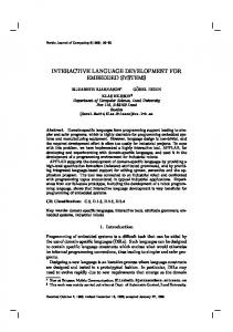
The device library contains for each device a description of its ports, interface properties, and low-level access routines. A device port is said to be guarded if it is able to isolate itself from a shared bus. A guarded port is not active unless its associated control signals, called guards, enable it. That is, the device does not sample or drive the guarded ports until the guard becomes true. The guards, by definition, are always active. As an example, the SCSI Controller shown in Fig. 2a has five ports that must be connected to a processor: DB (8-bit data port), ADDR (4-bit address port),
281
SynlhesizeInterface+ C F G s w , CFGHW, Devicefist, ProcessorList) foreach Processor E ProcessorList /I generate U 0 hardware and new software access routines SequencerList := SynthesizeSequencer(CFGsW ,CFGw w); DeviceList := DeviceList U SequencerList; I/ Fmt,use processor’s U 0 ports Connectedports := AlloclOPorts(Pmcessor, DeviceList); N Connect remaining ports with MMIO if (MMIO(Pmcessor, Devicefist - ConnectedPorts, IOPrefix) == fail) return fail; GenerateSoftwareO; retarn success;
CS (1-bit chip select), WR (1-bit writemode), and RD (1bit read mode). Port CS guards DB, ADDR, WR, and RD. To communicate with a peripheral device, the processor must generate a sequence of signals that read and write the device’s ports. These signal sequencings, called SEQs, are atomic routines that comprise a low-level procedural interface to the device. The SEQs can be viewed as a textual representation of the waveforms the processor will generate. SEQs are derived from the timing diagrams for the device’s interfaces and are customized to the capabilities of the processor in question [3]. SEQs are basic-block primitives. All control constructs such as loops and conditionals are expressed in higher-level device drivers. Another difference between SEQs and drivers is that only SEQs may directly access device ports whereas drivers must access them via calls to SEQs. Timing constraints can be specified on signaling events within a SEQ as well as between two SEQs invoked by a driver. Consider the example of a SEQ that writes a parameter to an internal register in the SCSI Controller (see Fig. 2b). First, the register’s address and the data to be written are placed on the ADDR and DE3 ports, respectively. Second, the chip is selected (enabled) by setting CS. Next, WR is pulsed to clock the data into the chip. Finally, the chip is deselected. 2.1.3 Control Flow Graphs At the high level, the behavioral description of the system is parsed and transformed into control flow graphs (CFGs) which call the device-drivers to perform YO. By default, the CFGs are implemented in software. The designer may tag portions of the CFGs to be implemented in hardware. These will be synthesized by a behavioral synthesis tool after an interfacing mechanism to software is added (i.e., an U 0 sequencer for passing input and output parameters). 2.1.4 Output The interface synthesizer outputs all the information necessary for the construction of the system. This includes a complete hardware netlist and software for the processors. In addition, the hardware output consists of interface glue logic modules described in structural Verilog to be synthesized by a behavioral compiler. The software output consists of access routines for all of the peripheral devices and U 0 sequencers. The access routines contain either I/O port instructions or load/store instructions mapped to I/O addresses. Using the output from the interface synthesizer along with the compiled control algorithms specified in the behavioral description, a designer can construct and powerup a fully functional system. 2.2 Main Algorithm The main algorithm (Fig. 3) is called with four parameters: C F G s w , C F G H W ,DeviceList, and ProcessorList. CFGsw is the set of control flow graphs to be implemented in software. CFGHW are the control flow graphs implemented in hardware and requiring I/O sequencers. DeviceList is the list of peripheral devices to be connected to the processors in ProcessorList. Each device is connected to one and only one processor and each processor may control multiple devices. The first step of the algorithm synthesizes hardware sequencers for C F G H ~and their access routines from
1 Fig. 3: Main algorithm for interface synthesis CFGsw . The next step allocates U 0 resources for the devices controlled by direct UO, including the newly synthesized sequencers. The algorithm first attempts to use I/O ports if the processor has them. If there are any unconnected device ports remaining, then the algorithm connects them using memory-mapped YO. Finally, the algorithm generates the device drivers by binding device ports in the SEQs to the U 0 resources of the processors. In the next section, we summarize the port allocation algorithm (described in detail in [11) and present a preprocessing step called port-width partitioning. Memory-mapped I/O and sequencer synthesis are described in sections 4 and 5 . 3 Interface Synthesisusing U 0 Ports The U 0 port allocation algorithm assigns processor U 0 ports for communication with peripheral devices. Interface synthesis using U 0 ports has been described in [11 with an O ( n 2 )greedy sharing heuristic, where n is the number of device ports. The algorithm assumes that oversized device ports, if any, have been partitioned manually. In this section, we review this algorithm, introduce a new automated port partitioning technique, and illustrate their application with an example. 3.1 U 0 Port Allocation The algorithm considers the n device ports in order of decreasing size. This order maximizes sharing opportunities among device ports. The greedy sharing heuristic is based on the observation that guarded ports from different devices cannot be simultaneously active and therefore may share the same U 0 port without multiplexing logic or a performance penalty. Unguarded device ports, including all guard ports, are always active, and so the algorithm allocates dedicated U 0 ports for them. If there are not enough I/O ports, the algorithm adds multiplexing logic to enable some unguarded device ports to share U 0 resources with other device ports. Two techniques for this areforced sharing and encoding transfomzation. Forced sharing adds a latch or a tristate, depending on the directionality of the device port, to free up a dedicated U 0 port, at the expense of a newly introduced guard signal. For single-bit device ports, such a scheme is actually a loss. Instead, encoding transformation adds a decoder or a multiplexor to encode the address for a group of single-bit ports. After the device ports have been allocated YO resources, the SEQs are customized to reflect the choice of processor ports and any interface logic that has been introduced. The algorithm outputs assembly code constituting the U 0 primitives for the higher-level device drivers.
282
MMIO(Processor e, DeviceList L , iohefix I)
t .......... ~
= 0, foreach (d E L ) { n =n+1, foreach @ E portList(d)) if (guarded@)) continue, if p can output or p used in reading seqs of d or allocateDataBits(d,p ) fails then allocateAddressBlts(d , p ) . avaIlDevSelect[dl = addrWidth( c) #usedAddrBits( d ) m= (#availDevSelect[z]), if (m 2 n) return one-hot-encode if (m 2 [lg(n)l) return binary-encode return Huffman-encode n
-
1 Fig. 5 : Memory-Mapped I/O Algorithm Fig. 4: Automatic I/O Port Allocationand Port-Splittingfor connecting an 8-bit Microcontrollerto a PC-Card Interface
pleting I/O ports, the algorithm introduces interface hardware to force some of the 8-bit ports to share the same processor I/O port. A multiplexor is used for reading singlebit output ports. A registered decoder is used to assert one control line at a time. 4 Memory-MappedYO Memory-mapped U 0 (MMIO) is attempted when 1/0 port allocation has failed due to the lack of 1/0 ports. Memory-mapped devices are accessed through the addresddata bus of the processor. This is more expensive than using I/O ports because it requires address matching logic. Yet, MMIO is less flexible than I/O ports because all accessing must be expressed in terms of load/store instructions, whereas I/O instructions allow for arbitrary sequencing. However, MMIO can be applied effectively to interfacing with a large class of devices when 1/0ports are not available. This section presents a technique for memorymapped 1/0 that introduces minimal address matching logic by efficiently assigningthe address bits to the devices. 4.1 Representation Input to the MMIO algorithm consists of a hardware template for the processor, a range of addresses reserved for I/O, and a list of devices to be connected. The output contains the address matching logic, connections made to the processor, and the updated SEQs for the devices. Each processor in the library has a template for translating memory control signals into a waveform required by the MMIO algorithm. It assumes that memory transactions have an address cycle followed by a data cycle. The address must be valid throughout both the address and data cycles. A pulse during the data cycle causes data to be either read or written. Each device is assigned a range of addresses. If the current memory transactionfalls within its address range, then it responds according to its inputs, which are connected to the address bus and the data bus. 4.2 Memory-mapped YO Algorithm The MMIO algorithm has several steps (Fig. 5). First, it ensures that every device port except the guards can share the memory bus by applyingforced sharing [l] if necessary. Second, all guarded device ports are assigned bits in the processor’s data port or the remaining bits in the address port. Third, it allocates address bits to uniquely identify each device, and generates the address matching logic.
3.2 Port-Width Partitioning The main port allocation algorithm assumes that none of the device ports are larger than the largest processor 1/0 port. If one is, then the preprocessing step described in this subsectiondivides it into several smaller ones, by introducing an interface component if needed. Many microcontroller families include processor versions with very different I/O port capabilities, hence, automating this task is necessary to facilitate experimentation with different processors. A device port is called splittable if it can be read or written in pieces without data consistencyproblems. For example, a touchtone generator is a combinational device with an input port that requires valid tone codes. Writing only to a slice of the input port may cause an invalid tone to be emitted. A register placed in front of the tone generator can act as a staging area for data delivered in slices. An output port is splittable if its value remains stable while the guard is true. Unguarded output ports are not splittable because the data values may change between sampling the different slices. Bidirectional device ports can be split using a register in each direction with complementary output enables. The device library contains an attribute that indicates whether a device port is splittable. 3.3 Example: U 0 Port Allocation after Device Port Splitting As an example where splitting ports is necessary consider connecting an 8-bit microcontroller directly to a PCCard bus, which is treated as a peripheral device (see Fig. 4). The PC-Card device has a 26-bit address port and a 16-bitbidirectional data port along with card enables CE1, CE2, and other control ports. Either CE1 or CE2 guards the remaining PC-Card ports. Therefore, the preprocessor partitions the address portintothree 8-bitports(ADDRO, ADDR1, ADDR2) and one 2-bit port (ADDR3). The data port is partitioned into two 8-bit ports (DATAO, DATA1). Note that, because of the guards, this is a logical partitioning and the ports require no extra hardware to make them splittable. The U 0 port allocation algorithm first attempts to dedicate processor U 0 ports to each of the 8-bit ports. Upon de-
283
Huffman-encode(DeviceL,istD ) { coast m = minjeo(#availDevSelectb]); L := 0; foreachi E D weight[i] := -#availDevSelect[i] m + 1; insert i into L while (ILI 2 2) {i, j } := extracth?in(L) k := makeTree(i, j ) weight[k] := weight[i]+weightlj]; insert k into L foreachi E D devSelect[d] := pathLabel(head(l), i)
Processor - -
+
Device Con"
data
*
!'ommeterr
-J
-
Dev.2
f
Fig. 6: Partitioning of the address space.
I The guard for each device is connected to the data strobe qualified by the output of its address matching bit. The memory-mapped architecture is shown in Fig. 6. Finally, the algorithm generates software from SEQs in terms of loadstore instructions. The MMIO algorithm partitions the address word into three fields: I/O prejix, device-select, and device-control. The I/O prejix field distinguishes I/O addresses from data memory addresses. Its width is fixed, possibly zero. The device-select field identifies devices within the YO address space. The device-control field, together with the data port, can be used to control the non-guard device pins. The algorithm must decide whether to assign each nonguard device port to either the device-control field or the data port. If the device port can output, then it must be assigned data bits. If the device port is input only, and if it is used in any SEQ that also reads any port from the device, then it must be assigned to the device-control field. This is because it must be written to with a load instruction, which reads from but cannot write to data pins. All other device ports may be allocated either way. The algorithm will attempt allocating data bits first in order to maximize the available device-select field, whose size is bounded by the remaining address bits after all other fields have been assigned. The device-select field is computed using one of three schemes, from the least expensive to the most expensive in terms of address matching logic: one-hot, binary, and Huffman encoding. If these schemes fail then the SEQs requiring the largest device-control field is divided into multiple transfers, thereby freeing address bits needed for the device-select field. In one-hot encoding, each device is selected by one address bit qualified by the I/O prefix. The advantage of this technique is that it requires very simple address comparator logic (an AND gate). A binary encoding technique of the device-select field encodes n devices with [log n1 bits. This technique frees ( n- [log n1) bits from one-hot encoding by using a single [log n1 input decoder to implement n address comparators. If the two approaches above fail, then the algorithm attempts Huffman encoding [4] of the device-select field. Huffman encoding uniquely identifies each device with a variable number of address bits. It exploits situations where the devices require different numbers of bits in the devicecontrol field. A device requiring more device-control bits is addressed by a shorter device-select pattern, and vice versa. The widths of the available device-control fields are used as the cost parameters to Huffman encoding (Fig.7). If a device has more available device-select bits, then it is
Fig. 7: Huffman Encoding assigned a smaller weight, which yields a longer Huffman encoding. If all three techniques fail to package the SEQs into single load/store instructions, then a transformation step divides the unpackageable SEQs into multiple memory instructions. This involves introducing registers and tristates to hold values for a subset of the ports in the SEQ. The remaining ports are accessed in subsequent load/store instructions. After all ports have been allocated, the MMIO algorithm generates the driver software by replacing the body of each SEQ with the appropriate memory operation(s).
4.3 Example: Wrist-watch Display by Memory Mapped YO We demonstrate the application of the MMIO algorithm with a video display on a wristwatch via an infrared link. The display is pieced together in quadrants using four square LCDs, each with 64x64 pixels. The peripherals include four LCDs and the IR receiving logic as well as an external 16K data memory connected to a Motorola 68hcll microcontroller. To illustrate the MMIO algorithm, only the data and address ports of the microcontroller are considered. The I/O prefix is given as zero in address bit 15 so the width of this field is one. The algorithm detects that the LCD's DB port is bidirectional and assigns it to the data port (Fig. 8). The RS and RW ports are input-only, used in reading SEQs, and are not guards. Therefore, they are assigned address bits 1 and 0 in the device-control field. The E port is a guard and is therefore connected to the output of the address comparator logic. Similarly for the receive logic, the control port is assigned address bits 5 through 0 and the DB port is assigned the data port. The remaining address bits are available for the device-select field. The one-hot test returns success because there are five memorymapped components and nine free bits. Fig. 9 shows how the software is updated. 4.4 Electronic Rolodex by Memory-Mapped YO This example demonstrates how the algorithm USGS Huffman encoding. It uses the 87c5 1 microcontroller without the I/O ports, an LCD, a tone generator, a 16K external RAM,a UART, and four individual switches. The UART is mapped to the built-in function. The other devices are memory-mapped.
284
.
tween signaling events. At the higher level, there may be response time and rate requirements. To meet these constraints, the designer or automated tools may move some functionality from software to hardware by tagging particular CFGs. For example, the infrared transmission prdtocol has intricate fine-grained timing constraints on the order of microseconds. Although it is possible to implement the protocol in software, a slow processor would not be able to service other devices at the same time. By creating a sequencer that implements the transmit protocol, the processor needs only to initiate a send command to the sequencer and can proceed to other tasks. This section describes the synthesis of this kind of hardware, which we refer to as VO sequencers. An VO sequencer communicates with a peripheral on behalf of the processor. In the simplest case, a sequencer is a slave FSM that waits for the processor to pass inparameters, invokes one of the SEQs, and returns outparameters, if any. This requires that the processor initiate every U 0 primitive. In the more sophisticated case, the sequencer autonomously interacts with the peripheral devices and the environment. The sequencer must in parallel communicate with the device and the processor. An example would be a sequencer that receives an infrared packet. This sequencer autonomously decodes the packet header, receives the specified number of bytes, calculates a checksum, and requests retransmission if necessary. After reading in the packet, the sequencer notifies the processor that a packet has arrived. After the I/O sequencer is synthesized, it is treated as a peripheral device to be connected to the processor using U 0 port allocation or MMIO. The input to the YO sequencer generator consists of the control flow graphs to be implemented in software (CFGsw) and hardware (CFGHW).The output is a synthesizable description of the hardware sequencer, the connection between the sequencer and the devices it controls, and the software routines called by CFGSw to access the sequencer. In addition to meeting performance requirements, the algorithm attempts to minimize the amount of hardware and the number of pins on the sequencer. We divide the problem into processor/sequencer protocol synthesis and finite state machine generation. 5.1 Algorithm for Sequencer Synthesis The algorithm generates an U 0 sequencer for each peripheral device that is accessed by a CFG tagged as hardware. An assumption of the algorithm is that if a device is accessed via a SEQ that must be implemented in hardware, then all of that device’s SEQs must also be implemented in hardware. The first step is to extract all entry points from the software into the hardware to be synthesized. For each peripheral device, the extracted entry points and the reachable CFGxw form an entry cluster. The algorithm transforms each cluster into an U 0 sequencer with customized access routines. First, it converts the hardware CFGs into FSMs using behavioral synthesis and then connects the FSMs to the corresponding peripheral device ports. The algorithm next synthesizes the communication protocol between the processor and the VO sequencer. The protocol involves selecting the appropriate entry point, passing the parameters, and synchronization between the processor and sequencer. Finally, the algorithm connects the protocol engine and the FSM, and updates the software entry points to reflect the synthesized
Fig. 8: Implementation of a wrist-watch display by one-hot encoded memory-mapped UO. SEQ Lcd-write (data) INPUT 1701 data;
1
SEQ Lcdl-write (data) INPUT [701dat&
1
.S:=1:
e:-&
address
/ / ewiii pu& automatidy
1
Original SEQ
Timing Diagram of Updated SEQ
Updated SEQ
Fig. 9: Updated SEQ after memory-mapping. First, the switches and the tone generator are not sharable, so the forced-sharing transformation is applied to make them sharable. Both one-hot and binary encodings fail because there are seven external devices (including the RAM)but only two address bits are available for the U 0 prefix and the device-select fields. Therefore the Huffman encoding technique is attempted. To perform Huffman encoding, the devices are sorted by the width of their device-control field. Note that the switches and the tone generator require no bits in the device-control field. A Huffman tree is created based on the widths of the device-control fields (see Fig. 10). This tree represents the VO prefix and device-select fields. These address bits are connected to the address comparator logic.
5 YO Sequencer Generation The chosen processor may not be able to satisfy all timing constraints by direct-VO. At the low level (SEQs), the constraints include minimum and maximum separation be1011 1010
1111
1110 110
100
0
RAM
0---
LCD
1001101011
TG
s1 s2 s3 54
iaio
1111 1110
Fig. 10: Huffman tree created for electronic rolodex along with the high order address bits required to select a device.
285
SynthesizeSequencer( CFGsw. CFGHW)
{
parameters for entry e param1 param2 param3
I
form entry clusters for each cluster generate FSM for CFGH w generate interface to device encode commands with required parameters generate param-latching FSM add transitions from paramFSM to CFGNW FSM update C F G s w
lDaramll1
Fig. 13: Determining the number of pins required for parameter passing Fig. 11: Algorithm for sequencer synthesis CFQa far inif and scaliw paramlcmmand FSM
I/O Sequencer Template
out
-sisn -~mrmnd
devN
-w-r
devl
dew
-~
d
y
protocol FSM
-
enlly FSM
Fig. 12: U 0 Sequencer template protocol. 5.2 Protocol Synthesis Protocol synthesis generates new SEQs for the processor to use to control the I/O sequencer as a peripheral device. These SEQs represent the new entry points into CFGHW. Note that the I/O sequencer must implement all communication between the processor and the peripheral device. Furthermore, it must also provide the processor with a means of obtaining status information for the sequencer. The template for a sequencer is shown in Fig. 12. Each entry point is encoded on the command port. Inparameters are passed in by selecting the appropriate entry point and pulsing the start signal. When invoking a call in the sequencer, the parameters can be transmitted individually or in groups. A protocol FSM reads in the parameters. The last parameter passed in kick-starts the selected entry’s FSM. While the FSM is executing, the ready bit is set false to prevent reentrant calls to the sequencer. Upon completion, the ready bit is set true. The processor can now read the out-parameters in a similar manner, The main problem in protocol synthesis is encoding the entry points and determining how to pass and retrieve parameters from the sequencer. Encoding of entry points may be done using techniques similar to encoding the deviceselect field in memory-mapped U 0 (section 4.2). Unlike memory-mapped YO, the parameters can be packaged many different ways from sending each parameter bit serially to passing all parameters simultaneously. The choice of a parameter passing protocol is influenced by timing constraints. The algorithm’s objective is to minimize the number of I/O sequencer pins required while still meeting timing constraints. The algorithm first determines W , the size of the
Fig. 14: Example of Sequencer Synthesis: Video Camera Scaler/Compressor with IR Transmitter parameter port. There are two things to consider, P,the number of time steps for passing parameters and Se the size of data to be transferred for each entry e (see Fig. 13). The width of the parameter port must allow all parameters to be transferred within the allotted number of time steps. Formally, the inequality W * P, 2 Se must hold for all entries e. Therefore, the algorithm chooses W such that:
5.3 Example: Video Camera with Scaling We illustrate the application of U 0 sequencers with a video camera which transmits images to a host via an infrared link. It digitizes a 256x256 8-bit grayscale image, scales it down to 128x128 pixels, applies video compression using frame differencing, and then transmits the image with the IR protocol. This system has many possible implementations. We consider a partitioning where an U 0 sequencer is introduced to perform scaling for the processor, in addition to handling interfacing with the digitizer. This partitioning allows the compression algorithm and the IR transmission protocol to be implemented entirely in software. On input to the sequencer synthesizer, the control flow graph for the scaler process has been tagged as hardware. This CFG accesses the digitizer, therefore all of the digitizer’s SEQs must be implemented as hardware as well. The first step of the algorithm forms the entry clusters by extracting the entry points from software. The four entries are initialization, enable-scaling, disable-scaling, and readpixel. For each cluster, the algorithm first generates the FSM for the CFGHW by calling behavioral synthesis on the scaler process and the SEQs it invokes. The algorithm connects this FSM to the peripheral device (the digitizer in this case). Next, the algorithm encodes the commands with the required parameters. Even though the digitizer’s
286
SEQs are also implemented in hardware, they are not directly invoked by software but rather through the sequencer and thus need not be encoded as separate commands. The only way for software to invoke the digitizer’s functions is through the four entry points into the scaler’s VO sequencer which are encoded using two bits in the command field. The initialization, enable-scaling, and disable-scaling commands require no parameters, while the read-pixel command transmits an 8-bit pixel to the processor. The state machine for handling parameter transmission and interfacing with the CFGHW is generated next. It has three main states. The first state waits for the processor to send a command. The next state sends the start signal to the corresponding entry in CFGHW.After the completion of the invoked entry, the third state waits for the processor to read the pixel before making a transition back to the first state. Finally, the algorithm generates the software to initialize the sequencer and to read a pixel using this synthesized protocol. The block diagram is shown in Fig. 14.
[21 P. Chou, R. B. Ortega, and G. Borriello. The Chinook Hardware/Software CO-Synthesis System. In Proc. ISSS, Sept. 1995. [3] P. Chou, E. A. Walkup, and G. Borriello. Scheduling for Reactive Real-Time Systems. In IEEE Micro, 14(4):37-47, August 1994.
[4] T. Cormen, C. Leiserson, and R. Rivest. Zntroduction to Algorithms. The MIT Press, 1990.
[5] R. Ernst, J. Henkel, and T. Benner. Hardware-software cosynthesis for microcontrollers. IEEE Design & Test of Computers, 10(4):64-75, Dec. 1993. [6] R. Gupta and G. De Micheli. Hardware-software cosynthesis for digital systems. Computers and Electrical Engineering, 10(3):29-41, Sept. 1993. [7] S . Narayan and D. D. Gajski. Interfacing system components by generation of interface processes. In Proc. 32nd DAC, June 1995.
6 Conclusion This paper presents a comprehensive set of techniques for the synthesis of hardware-software interfaces for embedded systems. Embedded system designers are challenged with meeting performance constraints while minimizing cost. Tools are needed to help designers explore the design space of possible solutions while being freed from the cumbersome tasks required for finalizing an implementation. This is crucial as it enables proper evaluation of design decisions early in the process. Synthesis of the interfaces between system components is one of these cumbersome tasks. An interface synthesis tool incorporating the techniques presented in this paper produces the glue logic and device drivers needed to connect processors to their peripheral devices. Hardware is introduced only when necessary for handling intricate timing constraints and for multiplexing U 0 resources. Once hardware decisions are finalized, device drivers are automatically customized to reflect the U 0 resource bindings and auxiliary hardware introduced. We presented U 0 port allocation and memory-mapped VO for allocating I/O resources found on general purpose microprocessors. Furthermore, we presented techniques for interfacing to elements of the system’s functionality that are implemented in hardware. This requires the synthesis of a parameter passing protocol that achieves the communication in the time allotted. These ideas have been validated with practical examples used throughout the paper, including several embedded systems that interact over an IR network. The techniques and algorithms presented in this paper are part of the Chinook co-synthesis tool for embedded systems under development at the University of Washington [2]. Future work includes development of interfacing techniques that permit sharing of communication resources between processors and interprocessor communication and synchronization mechanisms that will permit exploration of software/software partitions.
[8] M. Srivastava, B. C. Richards, and R. W. Brodersen. System level hardware module generation. IEEE Transactions on VLSISystems, 3(1), March 1995. [9] J. S . Sun and R. W. Brodersen. Design of system interface modules. In Proc. ICCAD, pp.478-481, Nov. 1992. [lo] M. Weiser. Some computer science issues in ubiquitous computing. CACM, 36(7):74-84, July 1993.
References [l] P. Chou, R. Ortega, and G. Borriello. Synthesis of the hardware/software interface in microcontroller-based systems. In Proc. ICCAD, pp.488-495, Nov. 1992.
287