Oct 10, 2012 - well created in the emitter region and the second localized in the main quantum well. We have also ...... Ministry of Science and Higher Education and its grants ... MacDonald, M. Sawicki, A. W. Rushforth, R. P. Campion,.
Intrinsic oscillations of spin current polarization in a paramagnetic resonant tunneling diode P. W´ ojcik, J. Adamowski,∗ M. Woloszyn, and B.J. Spisak
arXiv:1210.2280v2 [cond-mat.mes-hall] 10 Oct 2012
AGH University of Science and Technology, Faculty of Physics and Applied Computer Science, al. A. Mickiewicza 30, 30-059 Krak´ ow, Poland A spin- and time-dependent electron transport has been studied in a paramagnetic resonant tunneling diode using the self-consistent Wigner-Poisson method. Based on the calculated currentvoltage characteristics in an external magnetic field we have demonstrated that under a constant bias both the spin-up and spin-down current components exhibit the THz oscillations in two different bias voltage regimes. We have shown that the oscillations of the spin-up (down) polarized current result from the coupling between the two resonance states: one localized in the triangular quantum well created in the emitter region and the second localized in the main quantum well. We have also elaborated the one-electron model of the current oscillations, which confirms the results obtained with the Wigner-Poisson method. The spin current oscillations can lower the effectiveness of spin filters based on the paramagnetic resonant tunneling structures and can be used to design the generators of the spin polarized current THz oscillations that can operate under the steady bias and constant magnetic field.a PACS numbers: 72.25.Dc, 85.30.Mn
I.
INTRODUCTION
Dilute magnetic semiconductors (DMSs) such as ZnMnSe and GaMnAs are promising materials due to their potential applications in spintronics.1–7 The recent homo- and heteroepitaxy methods8–15 allow to deposit the DMS layers with thicknesses of few nanometers, which enables to fabricate spintronic nanodevices with the spin polarization of the current being controlled by the external magnetic and electric fields. The spin filter based on the DMS was proposed by Euges.16 The nanostructure studied in Ref. 16 consisted of a paramagnetic semiconductor layer made from Zn1−x Mnx Se sandwiched between two non-magnetic ZnSe layers. The external magnetic field leads to the giant Zeeman splitting of the conduction band minima in the paramagnetic layer, which causes that this layer acts as a potential well for spin-down electrons and a potential barrier for spin-up electrons. As a result, the total current flowing through the nanostructure is dominated by the spin-down electrons. In such a spin filter,16 the change of the spin polarization of the current requires the change of the external magnetic field. In the recently fabricated paramagnetic resonant tunneling diodes (RTDs)17–19 , the electrical control of the spin polarization of the current has been achieved. The spinpolarized current is controlled by the bias voltage in the presence of the external magnetic field in paramagnetic RTDs17,18,20,21 or even without the external magnetic field in ferromagnetic RTDs.22–27 If the quantum well in the RTD is made from the DMS, the spin splitting of the quasi-bound state energy level gives rise to the
a
To be published in Phys.Rev.B. Copyright (2012) by the American Physical Society.
resonant tunneling conditions for the spin-up and spindown electrons satisfied for different bias voltages. This leads to the separation of both the spin current components and consequently to the spin polarization of the net current. The operation of the paramagnetic RTD based on ZnSe/ZnBeSe/ZnMnSe heterostructure as a spin filter has been experimentally demonstrated by Slobodskyy et al.17 and theoretically described by Havu et al.28 Recently, the spin polarization of the current in the paramagnetic RTD has been reported at zero magnetic field.18 All these studies of the spin-polarized currents in the magnetic RTDs were devoted to the stationary (steady) currents. The oscillations of the spin-polarized currents in magnetic RTDs have not been studied until now, although the intrinsic oscillations of the current have been detected in the non-magnetic resonant tunneling structures.29–31 The intrinsic current oscillations occurring in the nonmagnetic RTDs are intensively studied due to their potential application as THz generators. Recently, the THz oscillations have been experimentally observed in the GaInAs/AlAs RTD integrated with a slot antenna.29–31 The attempts undertaken in order to explain the origin of these oscillations led to contradictory conclusions. Ricco and Azbel32 argued that the oscillations of the current in the non-magnetic RTD result from the fact that the system enters and leaves the resonant current conditions. According to this model,32 the intrinsic oscillations of the current should occur at the resonance bias that is in contradiction with the experimental29–31 and numerical33 studies, which show that the current oscillations occur only in the negative differential resistance (NDR) regime of the current-voltage characteristics, i.e., above the resonance bias. Woolard et al.34 suggested that the current oscillations in the non-magnetic RTD result from the charge fluctuations in the potential well created between the emitter and the nearest barrier. This proposition
2 was extended by Zhao et al.,35–37 who showed that the intrinsic oscillations are due to the coupling between the quasi-bound state localized in the emitter-related quantum well and the quasi-bound state in the main quantum well. However, this model35–37 is based on the adiabatic approximation, according to which the electron states are slowly varying in time. This assumption is not valid in the THz oscillation regime. Moreover, the explanation given by Zhao et al.35–37 does not answer the question, why the current oscillations do not decay in time as a result of the dissipative factor corresponding to the imaginary part of the resonance state energy. In our recent paper,38 we have shown that the intrinsic oscillations of the spin-unpolarized current result from the coupling between the two arbitrary quasi-bound states in the nonmagnetic triple-barrier resonant tunneling structure. We have found the intrinsic oscillations in two bias ranges. We have interpreted the oscillations that occur at the bias values below the resonance bias as resulting from the coupling between the quasi-bound states in both the quantum wells, while the oscillations that occur in the NDR regime as resulting from the coupling between the emitter-related quasi-bound state and the quasi-bound state localized in the nearby quantum well. In the present paper, we study the spin- and timedependent electronic transport in the paramagnetic double-barrier RTD based on ZnSe/ZnBeSe/ZnMnSe. We show that – under certain well-defined constant bias and external magnetic field – the intrinsic oscillations of both the spin current components appear, which leads to the oscillations of the spin polarization of the total current. Based on the analysis of the spin- and timedependent potential energy profiles and electron density distributions, we demonstrate that the oscillations of the spin polarized current result from the coupling between the quasi-bound state localized in the triangular quantum well created in the emitter (E) region with the spindependent quasi-bound state localized in the main quantum well (QW). The present results show that at certain bias voltages the spin polarization of the current flowing through the paramagnetic RTD is not constant but oscillates with the THz frequency. This effect can be of crucial importance for the possible applications of this nanodevice as a spin filter and THz generator. The paper is organized as follows: in Sec. II, we describe the theoretical model of the paramagnetic RTD and the time-dependent Wigner-Poisson method. Section III contains the results, Section IV – the discussion, and Section V – conclusions and summary.
II.
THEORETICAL MODEL
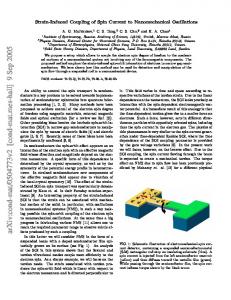
We consider the spin-dependent electronic transport through the paramagnetic RTD that consists of the paramagnetic quantum-well layer made from Zn1−x Mnx Se embedded between the two barrier layers made from Zn0.95 Be0.05 Se (Fig. 1). The active (undoped) region
of the nanodevice is separated from the n-doped ZnSe ohmic contacts by the two spacer layers made from ZnSe. In the presence of the external magnetic field B = (0, 0, B) applied in the growth (z) direction, the exchange interaction between the conduction band electrons and the Mn2+ ions leads to the giant Zeeman splitting of the conduction band minimum in the paramagnetic quantum-well layer.1 In the external magnetic field, the conduction-band electrons form the Landau states with the wave functions spread over the x − y plane. Therefore, the one-electron problem can be separated into (x, y) and z coordinates and the electronic transport between the emitter and collector can be described as the one-dimensional motion of the electron in the z direction.
FIG. 1. (Color online) Potential energy in the paramagnetic RTD for the electrons with spin-up (solid, red) and spin-down (dotted, blue). Coordinate z is measured along the growth direction, µE(C) is the electrochemical potential of the emitter (collector). The active (undoped) region consists of the paramagnetic quantum well made from Zn0.92 Mn0.08 Se sandwiched between the two Zn0.95 Be0.05 Se potential barriers and is separated from the n-doped ZnSe ohmic contacts by the two ZnSe spacer layers.
In order to simulate the electronic transport through the nanostructure, we apply the time-dependent WignerPoisson approach, according to which the conduction band electrons are described by the spin-dependent Wigner distribution function.39–41 The quantum kinetic equation takes on the following form39 ¯hk ∂ρW ∂ρW σ (z, k, t) σ (z, k, t) + (1) ∂t m ∂z +∞ Z i 0 = dk 0 Uσ (z, k − k 0 , t)ρW σ (z, k , t) , 2π¯h −∞
ρW σ (z, k, t)
where is the spin-dependent Wigner distribution function, k is the z-component of the wave vector, m is the electron conduction-band effective mass, and σ = (↑, ↓) is the spin index.
3 The non-local potential Uσ (z, k − k 0 ; t) for spin channel σ is given by the formula +∞ Z � Uσ (z, k − k , t) = dz 0 Uσ (z + z 0 /2, t) 0
(2)
−∞
� � � − Uσ (z − z 0 /2, t) exp − i(k − k 0 )z 0 , where Uσ (z, t) is the spin-dependent potential energy, which can be expressed as the sum of the two terms Uσ (z, t) = Uσcb (z, B) + Uel (z, t).
(3)
In Eq. (3), the first term denotes the spin-dependent potential energy of the conduction-band bottom, while the second term is the potential energy of an electron in the electric field acting in the nanostructure and has the form Uel (z, t) = UVb (z) + UH (z, t) ,
(4)
where UVb (z) is the potential energy of an electron in the electric field generated by voltage Vb applied between the emitter and collector and UH (z; t) is the Hartree energy that takes into account the electron-electron interactions. In Eq. (3), we have neglected the exchange energy (see Subsection IV.C). The conduction-band potential energy profile has the form U0 , if z1 ≤ z ≤ z2 and z3 ≤ z ≤ z4 , Uσcb (z, B) = ±EZ (B) , if z2 ≤ z ≤ z3 , 0, otherwise, (5) where z1 and z2 (z3 and z4 ) are the positions of the left (right) potential barrier interfaces, U0 is the height of the potential barrier, and EZ (B) is the Zeeman energy of an electron in the paramagnetic quantum-well layer, which is positive (negative) for the spin-up (spin-down) electrons. For a small concentration of Mn2+ ions the Zeeman energy can be expressed by the formula1 � � gµB SB 1 , (6) EZ (B) = N0 α x S0 BS 2 kB Teff where N0 α = 0.26 eV is the sp-d exchange constant, x is the concentration of Mn2+ ions, BS is the Brillouin function for spin S = 5/2 that corresponds to the spin of Mn2+ ion, g is the effective Land´e factor, µB is the Bohr magneton, S0 and Tef f are the phenomenological parameters corresponding to the antiferromagnetic interaction between the Mn2+ ions and have been taken on as S0 = 1.18 and Teff = 2.55 K for x = 0.083.42 Potential energy Uel (z, t) satisfies the Poisson equation d2 Uel (z, t) e2 = [ND (z) − n(z, t)] , dz 2 ε0 ε
(7)
where e is the elementary charge, ε0 is the vacuum electric permittivity, ε is the relative static electric permittivity, ND (z) is the concentration of the ionized donors,
P and n(z) = σ nσ (z) is the total density of electrons with nσ (z) being the density of the electrons with spin σ. The energy of the emitter conduction-band bottom is taken as the reference energy and set equal to 0. In order to solve the system of non-linear equations (1) and (7) we apply the self-consistent time-dependent procedure43 with the boundary conditions Uel (0, t) = 0 and Uel (L, t) = −eVb for the Poisson equation, where L is the length of the nanodevice. For the quantum kinetic equation (1) we apply the generalized form of the boundary conditions proposed by Frensley44 W = fσE (k) , (8) ρσ (0, k, t) k>0 = fσC (k) . ρW (L, k, t) σ k