as input to the Maxim MAX3872 clock and data recovery chip. ...... Harres, D., âNonlinear Processing of Manchester Data Corrupted by Multiplicative Noiseâ, ...
NRL Release Number 05-1226-2649
LABORATORY IMPLEMENTATION OF AN ADAPTIVE THRESHOLDING SYSTEM FOR FREE-SPACE OPTICAL COMMUNICATION RECEIVERS WITH SIGNAL DEPENDENT NOISE a b H. R. Burris , C. I. Moore , L. A. Swingenc, L. M. Wasiczkob, R. Mahond, M. F. Stella, M. R. Suiteb, W. S. Rabinovichc, J. L. Murphye, G. C. Gilbreathe, and W. J. Scharpfb a Research Support Instruments, 4325-B Forbes Blvd., Lanham, MD 20706 b Naval Research Laboratory, Code 8120, Advanced Systems Technology Branch, 4555 Overlook Ave. SW, Washington, DC 20375 c Naval Research Laboratory, Code 5650, Photonics Technology Branch, 4555 Overlook Ave. SW, Washington, DC 20375 d The Titan Corporation, 11955 Freedom Drive, Reston, VA 20190. e Naval Research Laboratory, Code 7210, Radio/IR/Optical Sensors Branch, 4555 Overlook Ave. SW, Washington, DC 20375 ABSTRACT The optimum detection threshold for optical communication receivers with large signal-dependant noise components can be derived from a Bayes’ Likelihood Ratio Test; however, the bit level statistics must be known a priori. In free-space communication systems, atmospheric conditions cause variations in optical transmission and subsequently in the bit level means and variances. These bit parameters must be tracked, estimated, and predicted, in order to update the detection threshold at a rate greater than the frequency of atmospheric changes. A laboratory implementation of an adaptive thresholding system is being implemented at the U.S. Naval Research Laboratory’s Chesapeake Bay Free-space Lasercom Testbed. Early results of experiments underway and initial design of the system will be presented. Keywords: optical communications; adaptive threshold; free-space lasercom.
1. INTRODUCTION It is well known that the optimum detection threshold for optical receivers with large signal dependant noise components is not simply the average value of the high and low bit currents (or zero for ac coupled detectors). The optimum detection threshold in this type of system is derived from a Bayes' likelihood ratio test (LRT) and is a function of the bit level means and variances; therefore, it will not be constant under varying transmission conditions [1,2]. Optical detectors exhibiting this characteristic are avalanche photodiodes (APD’s) and photomultipliers as well as PIN photodiodes coupled with optical preamplifiers [2,3,4,5]. The derivation of the detection threshold requires a priori knowledge of the mean and variance of the bit levels. In free-space optical communication links a priori knowledge of the signal statistics will be problematic. An adaptive method that can track the changes in the mean and variance of the signal bits, and update the detection threshold is needed in order to implement the signal dependant noise Bayesian LRT detection threshold [3,6]. NRL has begun the implementation of a system for testing the characteristics of optical receivers expected to have large signal-dependant noise components and to ultimately adaptively control the detection threshold for near optimum bit error rate performance.
2. BACKGROUND In free-space optical communication (FSO) systems, it is usually desirable to have the sensitivity of the detector as high as possible to reduce the required laser power for a specified link margin. However, the optical receivers used for high speed optical communication systems that operate closest to the quantum limit are the PIN diode coupled to an optical fiber preamplifier and an APD. Both of these devices have large multiplicative noise components that cannot be ignored. As stated above, the optimum detection threshold for an optical detector with signal dependant noise that cannot be ignored can be derived from a Bayes’ Likelihood Ratio Test [7,8]. The expression for the optimum threshold is
Free-Space Laser Communications V, edited by David G. Voelz, Jennifer C. Ricklin, Proc. of SPIE Vol. 5892 (SPIE, Bellingham, WA, 2005) · 0277-786X/05/$15 · doi: 10.1117/12.622298
Proc. of SPIE 58920W-1
Form Approved OMB No. 0704-0188
Report Documentation Page
Public reporting burden for the collection of information is estimated to average 1 hour per response, including the time for reviewing instructions, searching existing data sources, gathering and maintaining the data needed, and completing and reviewing the collection of information. Send comments regarding this burden estimate or any other aspect of this collection of information, including suggestions for reducing this burden, to Washington Headquarters Services, Directorate for Information Operations and Reports, 1215 Jefferson Davis Highway, Suite 1204, Arlington VA 22202-4302. Respondents should be aware that notwithstanding any other provision of law, no person shall be subject to a penalty for failing to comply with a collection of information if it does not display a currently valid OMB control number.
1. REPORT DATE
3. DATES COVERED 2. REPORT TYPE
2005
00-00-2005 to 00-00-2005
4. TITLE AND SUBTITLE
5a. CONTRACT NUMBER
Laboratory Implementation of an Adaptive Thresholding System for Free-Space Optical Communication Receivers with Signal Dependent Noise 6. AUTHOR(S)
5b. GRANT NUMBER 5c. PROGRAM ELEMENT NUMBER 5d. PROJECT NUMBER 5e. TASK NUMBER 5f. WORK UNIT NUMBER
7. PERFORMING ORGANIZATION NAME(S) AND ADDRESS(ES)
Naval Research Laboratory,Code 8120, Advanced Systems Technology Branch,4555 Overlook Ave SW,Washington,DC,20375 9. SPONSORING/MONITORING AGENCY NAME(S) AND ADDRESS(ES)
8. PERFORMING ORGANIZATION REPORT NUMBER
10. SPONSOR/MONITOR’S ACRONYM(S) 11. SPONSOR/MONITOR’S REPORT NUMBER(S)
12. DISTRIBUTION/AVAILABILITY STATEMENT
Approved for public release; distribution unlimited 13. SUPPLEMENTARY NOTES 14. ABSTRACT
The optimum detection threshold for optical communication receivers with large signal-dependant noise components can be derived from a Bayes? Likelihood Ratio Test; however, the bit level statistics must be known a priori. In free-space communication systems, atmospheric conditions cause variations in optical transmission and subsequently in the bit level means and variances. These bit parameters must be tracked, estimated, and predicted, in order to update the detection threshold at a rate greater than the frequency of atmospheric changes. A laboratory implementation of an adaptive thresholding system is being implemented at the U.S. Naval Research Laboratory?s Chesapeake Bay Free-space Lasercom Testbed. Early results of experiments underway and initial design of the system will be presented. 15. SUBJECT TERMS 16. SECURITY CLASSIFICATION OF: a. REPORT
b. ABSTRACT
c. THIS PAGE
unclassified
unclassified
unclassified
17. LIMITATION OF ABSTRACT
18. NUMBER OF PAGES
Same as Report (SAR)
20
19a. NAME OF RESPONSIBLE PERSON
Standard Form 298 (Rev. 8-98) Prescribed by ANSI Std Z39-18
γ=
σ 0 ⋅σ 1 ⋅ σ 12 − σ 02
( µ1 − µ0 )
2
( )
µ ⋅ σ 2 − µ1 ⋅ σ 02 + 2 ⋅ (σ 12 − σ 02 ) ⋅ ln σ 1 σ + 0 12 σ −σ 2 0 1
(1)
0
in which µ0 and µ1 are the mean signal currents of the low and high bits respectively and the σ02 and σ12 are the respective variances. If the signal dependant noise is negligible as it is in a standard PIN diode (with no optical amplifier), σ02 and σ12 are approximately equal and the Eqn. (1) will reduce to the average value of µ0 and µ1. This approximation is the equal variance threshold (EVT). 2.1 Multiplicative (Signal-dependant) Noise In a typical optical receiver such as a PIN diode, the received signal is a Poisson random process. The probability of receiving n photons during a single bit interval is
pn = e
(
− Pr
h⋅ν c ⋅Rb
)⋅
⎛ ⎞ Pr ⎜ ⎟ ⎝ h ⋅ν c ⋅ Rb ⎠
n
(2)
n!
in which Pr is the received power, h is Planck's constant, νc is the frequency of the optical carrier, and Rb is the bit rate [9,10,11]. An ideal receiver for an ideal on-off keying (OOK) modulation scheme will therefore make no errors for the 0 bits when the light is turned off. During a 1 bit, the receiver will have a probability of receiving 0 photons of
pn =0 = e
(
− Pr
h⋅ν c ⋅Rb
)
(3) where the exponent represents the average number of photons received during one bit period. If the probability of sending a 1 and a 0 are the same, then the ideal error probability, or bit error rate is
BER = 1 ⋅ e 2
(
− Pr
h⋅ν c ⋅Rb
).
(4)
This expression is the quantum limit of an ideal detector in an ideal OOK modulation scheme. For example, a BER of 10-8 will require approximately 18 photons per 1 bit [10,11]. However, practical, non-ideal receivers have noise present and typical high speed modulators are not ideal in that the low bits do not correspond to a power level of zero [11]. The two types of optical receivers that can have sensitivities closest to the ideal quantum limit are the PIN diode coupled to an optical preamp and the avalanche photodiode (APD) [10]. Both of these detectors have large, non-negligible multiplicative noise sources. In long distance freespace optical systems, where transmitter power budget and eye-safety are important issues, it is important to have receiver detectors with very high sensitivity; thus, the APD and preamp coupled PIN diode are usually the detectors of choice. In a typical PIN diode receiver with an electronic transimpedance amplifier (no optical preamp), the dark current is usually extremely small and is considered negligible; therefore, the noise sources that are considered when analyzing performance are thermal noise, shot noise, and amplifier noise. Thermal noise is modeled as a zero mean, white, Gaussian random process with a thermal noise current variance of
(
)
σ th 2 = 4 ⋅ k B ⋅ T R ⋅ Be L
(5)
where kB is Boltzmann's constant (1.38 x 10⁻²³ J/K), RL is the resistor value, T ( in K) is the temperature, and Be is the electronic bandwidth. This is usually the dominant noise source for PIN diode detectors. Shot noise is the representation of the random nature of the photoelectron generation process. As described above, the process is governed by Poisson statistics; however, at the signal powers present in optical communication systems, Gaussian statistics are a very close approximation and are generally used due to the simplification of analysis [11]. The photocurrent with shot noise can be modeled as:
I = I + is
(6)
where I is the constant average current and is is a zero mean, Gaussian random variable representing the shot noise variability. For PIN diodes, the shot noise current variance is:
σ sh = 2 ⋅ e ⋅ I ⋅ Be = 2 ⋅ e ⋅ ( Rpin ⋅ Pr ) ⋅ Be 2
(7)
where Rpin is the PIN diode responsivity and Pr is the received optical power [10,11]. Since the thermal noise and shot noise are assumed to be independent, the total photocurrent variance is the sum of the two variance terms above. Note
Proc. of SPIE 58920W-2
that even the PIN diode has shot noise variance that is proportional to the received signal power, Pr; however, in all practical receivers, the noise is dominated by the thermal noise such that the signal dependent shot noise is typically negligible. The front-end amplifier noise contribution is usually included in the noise Figure, Fn, of the amplifier. The noise figure is the degree to which noise present at the amplifier input is enhanced by the amplifier. Therefore, at the amplifier output of a typical PIN diode with transimpedance amplifier, the photocurrent variance will be:
(
)
σ total 2 = 4 ⋅ k B ⋅ T R ⋅ Fn ⋅ Be L
(8)
where RL is the load resistor [10,11]. Again, this assumes that the signal dependent shot noise is negligible which is usually the case. Therefore, in optical communication systems that use a PIN diode with a front-end transimpedance amplifier, the multiplicative (or signal dependent) noise is typically not considered. However, a PIN diode with electronic transimpedance amplifier has a sensitivity of at least one order of magnitude less than that of an APD, and at least two orders of magnitude less than that of a PIN diode coupled to an optical preamplifier [10,11]. Therefore, in free-space optical communication systems where transmitted power is at a premium, the receivers usually take advantage of the increased sensitivity of the APD or PIN diode / optical preamp combination. The APD has an increased shot noise due to the avalanche gain process. The APD shot noise current variance is modeled as:
σ sh,apd 2 = 2 ⋅ e ⋅ Gm 2 ⋅ F (Gm ) ⋅ R ⋅ Pr ⋅ Be
(9)
where Gm is the avalanche multiplication gain, R is the detector responsivity at a gain of 1, and F(Gm) is the excess noise factor which is a function of the avalanche gain. The APD shot noise is typically modeled as a zero mean, Gaussian process at the signal levels encountered in optical communication systems. The excess noise factor is given by:
(
F ( Gm ) = k A ⋅ Gm + (1 − k A ) ⋅ 2 − 1
Gm
)
(10)
where kA is the ionization coefficient which is a property of the semiconductor material used in the APD and has a range of 0 to 1. In silicon APD's which can be used up to an optical wavelength of ~ 1100nm, the ionization coefficient can be kept fairly small (typically ~ 0.1). However, for optical wavelengths above ~ 1100nm, such as 1330nm and 1550nm which are of particular interest for freespace links since these are in the "eye-safe" wavelength region, other semiconductor materials such as InGaAs must be used. InGaAs APD's have an ionization coefficient much higher than that of silicon, typically in the vicinity of ~ 0.4 to 0.7 [10,11]. Therefore, since the signal dependent shot noise in APD's is multiplied by an additional factor of Gm ⋅ F ( Gm ) , the shot noise in these devices will typically dominate over 2
thermal noise and cannot be neglected. In the PIN diode / optical preamp receiver, there will be additional current noise variance terms due to the beating of the spontaneous noise power produced in the optical amplifier with itself and with the received optical signal. These noise terms can also be adequately modeled as Gaussian processes and, at typical optical amplifier gains, will be the dominant noise terms over both thermal noise and shot noise. The signal-spontaneous beat noise produces a noise current variance of:
σ sig − spont 2 = 4 ⋅ R 2 ⋅ Go ⋅ Pr ⋅ Pn ⋅ ( Go − 1) ⋅ Be (11) where Go is the optical amplifier gain and Pn = nsp ⋅ h ⋅ν c , in which h is Planck's constant, ν c is the optical frequency,
and nsp is the spontaneous emission factor (typically in the range of 2 to 5) [10]. The spontaneous-spontaneous beat noise produces a noise current variance of:
σ spont −spont 2 = 2 ⋅ R 2 ⋅ ⎡⎣ Pn ⋅ ( Go − 1) ⎤⎦ ⋅ ( 2 ⋅ Bo − Be ) ⋅ Be 2
(12)
in which Bo is the optical bandwidth of the system, usually determined by optical bandpass filters. In practice, to reduce the system noise and improve performance, the spontaneous-spontaneous noise term can usually be reduced to a very small level with optical filters so that the dominant noise term is always the signal-spontaneous beat noise. As can be seen above, this dominant noise term is also proportional to the received optical power. As shown above, the most sensitive detector configurations for freespace optical communication systems have large multiplicative (signal dependent) noise variances that cannot be ignored. Although the PIN-diode-optical-preamp receiver has sensitivity closest to the quantum limit, the APD receiver has a much wider use in FSO systems. Currently, optical preamplifiers are typically constructed with single-mode optical fiber. In freespace optical systems, turbulenceinduced spot motion makes coupling of received light into a single-mode fiber extremely difficult without the use of
Proc. of SPIE 58920W-3
expensive adaptive optics techniques and the sensitivity gain is canceled by the coupling. Although there has been recent work in the development of optical fiber preamps using multimode fiber, the initial thrust of the NRL work concentrates on systems using APD detectors. 2.2 Previous theoretical results Atmospheric turbulence can cause the average received power to fluctuate with power spectrum components in the kilohertz regime. Therefore, the received bit signal currents and their variances fluctuate as well. In order to maintain the receiver detection threshold at near-optimum, these bit-level means and variances must be tracked and estimated. A block diagram of a proposed solution is shown below in Figure 1.
D E
~ Gbps DATA RATE
OPTICAL RECEIVER w/ MULTIPLICATIVE NOISE
SUFFICIENT STATISTIC
C THRESHOLD COMPARISON
I S I
ADAPTIVE MEAN & VARIANCE PREDICTOR
THRESHOLD UPDATE
~ 1 kHz RATE
O N
DECISION FEEDBACK
1: Figure 1: Adaptive System Block Diagram
Previous work has involved theoretical comparisons of bit error rates obtainable with the optimum Bayesian LRT detection threshold and the equal variance threshold. An example of this sort of analysis is shown in Figure 2 in which it can be seen that more than an order of magnitude improvement can be obtained with the adaptive LRT threshold [7,8]. These past efforts [7,8] have concentrated on development of adaptive predictor algorithms that can predict the mean and variance values and maintain the detection threshold near optimum. Adaptive algorithms have been developed based on Kalman Filters, Least Mean Squares adaptive predictors, and a Modified Sequential Regression adaptive algorithm. It has been demonstrated with simulation studies that these adaptive predictors can yield BER performance at the theoretical limit, with order-of-magnitude improvement over the EVT threshold performance. Figure 3 shows a comparison of the three adaptive predictors’ BER performance to the theoretical limit. Figure 4 is a comparison of the Kalman Filter adaptive predictor BER performance to that of the EVT threshold. The results were generated with simulated bit data superimposed on actual power fade rate data taken at the NRL Free-space Lasercomm Test Facility at Chesapeake Beach, MD [7,8].
Proc. of SPIE 58920W-4
Theoretical Bit Error Rate Comparison 1 0.1
EVT
BER
0.01 1 . 10
3
1 . 10
4
1 . 10
5
1 . 10
6
1 . 10
7
1 . 10
8
Adaptive LRT
1
10 100 Average SNR Figure 2: Comparison of theoretical bit error rate curves for the adaptive LRT and the EVT. The upper solid curve is the BER curve for a EVT type threshold (equal variances). The lower dashed curve uses a Bayes’ LRT threshold.
C om parison - 2msec ave Adaptive BER Predictor BER Comparison 1 .00E+00 0
0 .01
0.02
0 .0 3
0.04
0 .0 5
0.06
0 .07
0.08
0 .0 9
0 .1
1 .0 0E-01
Bit Error Rate
1 .0 0E-02
Theo retical
1 .0 0E-03
0 Errors Kalman Filte r LM S 1 .0 0E-04
SER
1 .0 0E-05
0 Errors 1 .0 0E-06
1 .0 0E-07
Theoretical Time (s ec)
Figure 3: Comparison of Theory, Linear State Model Kalman filter, LMS predictor and Modified Sequential Regression predictor bit error rate performance; averaged over 2msec time intervals.
Proc. of SPIE 58920W-5
Kalman Filter to Matched Filter - BER Comparison
Kalman Filter / EVT : BER Comparison 1.00E+00 0
1.00E-01
0.01
0.02
0.03
0.04
0.05
0.06
0.07
0.08
0.09
0.1
EVT
Bit Error Rate
1.00E-02
1.00E-03
1.00E-04
1.00E-05
Kalman Filter
0 Errors 1.00E-06
1.00E-07 Time (sec)
Figure 4: Comparison of Kalman filter BER performance with the EVT.
The previous theoretical results have led to the current effort at NRL to develop a laboratory testbed to characterize candidate optical detectors and to implement and evaluate adaptive thresholding techniques.
3. ADAPTIVE THRESHOLDING TESTBED DEVELOPMENT The NRL free-space lasercomm program has an ongoing development effort for receiver detectors that either have no fiber pigtail or a multimode fiber pigtail to enable receivers with reasonable link margins without the use of complicated and expensive adaptive optics systems. The development effort involves investigation of commercial detectors with high responsivity at 1550nm, as well as cooperative efforts with other organizations for development of InGaAs detectors with improved response and noise characteristics. In support of this effort, the adaptive thresholding testbed has been designed to allow characterization and testing of both free-space detectors and multimode fiber pigtailed detectors. 3.1 Characterization of fiber pigtailed optical detectors A general block diagram of the testbed as used for fiber pigtailed detectors is shown in figure 5. An Agilent 86130A 3.6 Gb/s Error Performance Analyzer is the heart of the system. The Agilent BER tester provides the electronic output data signal at data rates up to 3.6 Gb/s with selections of pseudo random bit sequences for testing. The output of the Agilent pattern generator is applied to a commercial OC-48 transmitter from Optical Communication Products (OCP). The transmitter module output is a
Proc. of SPIE 58920W-6
Kingfisher KI7010A Optical Attenuator
2
Recovered Data 2
1. 5
1
Volts
OCP OC-48 Optical Transmitter Module
Yj 0. 5
0
0. 5 −1 1 0 0
5.10
6
1. 10
5
1. 5.10
5
2. 10
5
2. 5.10
j
5
3 .10
5
3. 5.10
5
4 .10
5 −5
TDS 5052 DSO Scope
4×10 7
5⋅10 Tim e (sec)
Agilent 86130A 3.6Gb/s Error Performance Analyzer Transmitter / Pattern Generator
Optical Receiver Under Test
Receiver / Error Detector Analog Devices AD5541 16 bit Precision DAC
Threshold Voltage
Threshold Voltagevs InputPower 0.008 0.006 0.004 0.002 0 0.3
0.4
0.5
0.6
0.7
0.8
Relative Input Power
GPIB
Data In
0.9
1
Laptop Threshold Control & BER Data Acq
Maxim MAX3872 Clock & Data Recovery Board with Adjustable Detection Threshold
+
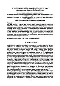
Figure 5: Fiber pigtailed detector characterization system block diagram.
nominal 1 milliwatt at 1548nm with a nominal extinction ratio of 10 dB (8.2 dB minimum). The output of the OCP OC48 transmitter is passed through a Kingfisher International KI 7010A optical attenuator. The KI 7010A has an attenuation range of 2 to 60 dB with a resolution of 0.05dB. The attenuator’s power handling capability is 30 dBm. The output of the KI 7010A was calibrated with a Newport model 850 power meter with an integrating sphere detector head. The attenuated optical signal is applied to the fiber pigtailed detector under test. If the detector being tested has differential outputs, one of the outputs is monitored on a Tektronix TDS5052 oscilloscope, while the other output is used as input to the Maxim MAX3872 clock and data recovery chip. The MAX3872 is a multirate clock and data recovery (CDR) chip with built in limiting amplifier designed for OC-3, OC-12, OC-24, OC-48, and Gigabit Ethernet applications. The chip has a fully integrated phase locked loop for clock recovery from serial NRZ input data, and differential data inputs as well as differential recovered clock and data outputs. It also has a vertical threshold control voltage input for compensating for signal dependant noise from the detector. In our testbed, a precision DAC board from Analog Devices supplies this control voltage input. The DAC board is an AD5541 evaluation board with a built in AD780 +2.5 volt precision voltage reference and a high precision OP-97 buffer amplifier. The AD5541 provides a unipolar, 16 bit output for setting the detection threshold of the MAX3872. The transfer curve of the control voltage of the MAX3872 is shown in figure 6. The AD5541 evaluation board is controlled from
Proc. of SPIE 58920W-7
Vthreshold (mV) +170
Vctrl (V) 1.2
0.3
2.1
-170 Figure 6: MAX3872 control voltage transfer curve.
the parallel port of a laptop computer that also acquires the bit error rate data from the Agilent BER tester over GPIB. The MAX3872 board supplies the recovered data signal to the Agilent error detector for BER testing. Since the testbed is located on a single tabletop, the clock from the Agilent pattern generator is routed directly to the error detector; however, the clock recovery capabilities of the MAX3872 have been tested and could be used for the clock of the error detector if desired. The laptop computer controls the setting of the detection threshold of the MAX3872 CDR chip and obtains data from the Agilent BER tester under Labview control. In the preliminary testing that has been performed so far, the software has been set to increment the control voltage in steps of 100 microvolts and to obtain from 500 to 10,000 Delta BER readings from the BER tester for each detection threshold setting. As the optical input power to the detector is increased, the bit error rate decreases, requiring more Delta BER readings from the Agilent BER tester for accuracy. The average optical input power to the detector under test was varied in increments of 0.5 dB. At each average power setting, a range of detection threshold values was used, with BER determinations at each threshold setting. This allows determination of the optimum detection threshold for the applied average input power with good confidence at BER levels above ~ 10-8. When the BER is below ~ 10-8, the data collection becomes very tedious due to the infrequent nature of the errors, even when testing at rates of 2.5 Gb/s. Initial testing has been done on two multimode fiber pigtailed detectors: a DSC-R102APD-DC-73-FC/UPC-K from Discovery Semiconductors and a TriQuint P173A OC-48 APD receiver. The DSC-R102APD from Discovery is an InGaAs APD with a 3dB roll off frequency of 0.95 GHz and a rated responsivity of 0.7 A/W at 1550nm at a gain of 1. It has a breakdown voltage of 45.7 volts and an integral transimpedance amplifier with transimpedance of 500 ohms. The DSC-R102APD output was input to a MAX3872 CDR evaluation board described above for testing. The Triquint APD is an InGaAs APD with a breakdown voltage of 38.6 volts and a typical sensitivity of –34 dBm for a 10-10 BER at 2.5 Gb/s. The Triquint detector has a minimum responsivity of 0.75 A/W at a gain of 1 and a bandwidth of 2.6 GHz. It also has an integral transimpedance amplifier with transimpedance of 4000 ohms. The Triquint detector was built into an optical receiver module with a bandwidth limiting filter and a MAX3872 CDR chip. 3.2 Preliminary results Early results from the initial testing of the DSC-R102APD and the Triquint based detector are shown in figures 7 through 11 below. Figure 7 is an example of the data collected using the testbed shown in figure 5. As can be seen in the right hand data plot of figure 7, as the input power to the device under
Proc. of SPIE 58920W-8
BERData, DSC-R102APD, Vapd=44.5V Input Power =-28.12 dBm
BERData, DSC-R102APD, Vapd=44.5V Input Power =-25.11dBm
1.0E-03
Bit Error Rate
Bit Error Rate
1.0E-07
1.0E-08
1.0E-04
1.0E-05 5.0E-04
1.0E-03
1.5E-03
2.0E-03
2.5E-03
3.0E-03
3.5E-03
1.0E-09 1.0E-03
1.2E-03
1.4E-03
1.6E-03
1.8E-03
2.0E-03
2.2E-03
2.4E-03
2.6E-03
2.8E-03
ThresholdVoltage
ThresholdVoltage
Figure 7: Examples of the BER data versus threshold voltage obtained from the testbed shown in figure 5 for determining the optimum control voltage (or threshold voltage) for two different received power levels for the DSCR102APD. The two power levels shown are –28.12 dBm (left) and –25.11 dBm (right). Testing of other devices is being performed in the same manner.
Optimum Threshold Voltage DSC-R102, Vapd = 44.5V, Vbrk = 45.7V
Optimum Control Voltage DSC-R102, Vapd = 44.5V, Vbrk = 45.7V
O p tim um T hre sho ld
O ptim um C on tro l V o ltage
1.1940 1.1930 1.1920 1.1910 1.1900 1.1890 1.1880 -32
-30
-28
-26
-24
2.3E-03 2.1E-03 1.9E-03 1.7E-03 1.5E-03 1.3E-03
-22
Received Power (dBm)
-32
-30
-28
-26
-24
-22
Received Power (dBm)
Figure 8: Measured optimum control voltage and calculated optimum threshold voltage for the DSC-R102APD for bias voltage value of 44.5 volts.
test is increased and the bit error rate decreases, it becomes necessary to obtain larger amounts of data for a reasonably smooth BER versus threshold voltage curve that will show an obvious minimum. Unfortunately, this region of low BER is the most critical region for determination of the optimum threshold since this is where the BER curve for a Likelihood Ratio Test (LRT) diverges away from that of an Equal Variance Threshold (EVT) detector. In the future, it will be attempted to fit a curve through the noisy data set to improve the optimum threshold determination.
Proc. of SPIE 58920W-9
BER Comparison - Vopt vs Vc = 1.186V DSC-R102, Vapd = 44.5V, Vbrk = 45.7V 1.0E+00 1.0E-01
Bit Error Rate
1.0E-02 1.0E-03 1.0E-04 1.0E-05 1.0E-06 1.0E-07 1.0E-08 1.0E-09 1.0E-10 1.0E-11 -33
-31
-29
-27
-25
-23
Received Power (dBm)
BER Comparison - Vopt vs Vc = 1.1885V DSC-R102, Vapd = 44.5V, Vbrk = 45.7V 1.0E+00
Bit Error Rate
1.0E-01 1.0E-02 1.0E-03 1.0E-04 1.0E-05 1.0E-06 1.0E-07 1.0E-08 1.0E-09 1.0E-10 1.0E-11 -33
-31
-29
-27
-25
-23
Received Power (dBm)
Bit Error Rate
BER Comparison - Vopt vs Vc = 1.193V DSC-R102, Vapd = 44.5V, Vbrk = 45.7V 1.0E+00 1.0E-01 1.0E-02 1.0E-03 1.0E-04 1.0E-05 1.0E-06 1.0E-07 1.0E-08 1.0E-09 1.0E-10 1.0E-11 -33
-31
-29
-27
-25
-23
Received Power (dBm)
Figure 9: Comparison of bit error rates obtained using the measured optimum control voltage (threshold voltage) versus constant control voltage values for the DSC-R102APD at Vapd voltage of 44.5 volts.
Figure 8 contains a graph of the measured optimum control voltage of the DSC-R102APD at a bias voltage of 44.5 volts and a graph of the optimum threshold voltage calculated from the control voltage using the transfer characteristic shown in figure 6. Figure 10 contains the graphs of the measured optimum control voltage and the calculated threshold voltage for the Triquint receiver. Note that the full range of the threshold voltage of the DSC-R102 is only ~ 0.8 millivolts while the full range of the control voltage is ~ 5 millivolts. The Triquint receiver curves of figure 10 indicate a threshold voltage range of ~ 1.9 millivolts and a control voltage range of ~ 9 millivolts, possibly indicating a larger amount of multiplicative noise. This difference will be discussed in more detail in section 4 below. A very small control voltage adjustment range was expected; this is the reason that the AD5541 DAC with a precision voltage reference and a least-
Proc. of SPIE 58920W-10
significant-bit resolution of 38 microvolts was used. Although the MAX3872 CDR chip fits readily into the adaptive thresholding scheme, it may not be useable for the final system. Unfortunately, according to the specifications from Maxim, the MAX3872 threshold control voltage transfer characteristic can shift up or down by as much as 10% with temperature and power supply fluctuations. Future testing will determine if it can be used in the system. Optim um Threshold Voltage - Triquint Receiver Vapd = 35V
1.211 1.210 1.209 1.208 1.207 1.206 1.205 1.204 1.203 1.202 1.201 1.200
0.00E+00 V threshold (Volts)
V control (Volts)
Optimum Control Voltage - Triquint Receiver Vapd = 35V
-40
-38
-36
-34
-5.00E-04 -1.00E-03 -1.50E-03 -2.00E-03 -40
-38
-36
-34
Received Pow er (dBm)
Received Power (dBm)
Figure 10: Measured optimum control voltage and calculated optimum threshold voltage for the Triquint receiver for bias voltage value of 35 volts.
Figures 9 and 11 show comparisons of bit error rate obtained with the measured optimum control voltage for the various input power levels, versus the bit error rate obtained with a constant control voltage for three different values of control voltage selected from either extreme and from the middle of the measured optimum control voltage range. Figure 9 is the curve for the DSC-R102 while figure 11 is for the Triquint receiver. In both figure 9 and 11, the top graph is a comparison between the LRT threshold result and the EVT threshold result. Examination of the graphs in both figures indicates an improvement in BER when using the optimum control voltage (more so in figure 11 than in figure 9); however, it is also seen that a control voltage can be picked near the center of the measured range (middle graph of both figures) that will give BER performance very close to that of the optimum. Theoretical data will be presented in section 4 below that indicate possible reasons for the close proximity of the optimum BER curve and a non-optimum curve. The data for the DSC-R102 was taken at 1.06 Gb/s. The data for the Triquint receiver was taken at OC-48 rates (~2.488 Gb/s). In general, the closeness of the BER curves indicates that the noise is not totally dominated by signal dependent noise; i.e. the additive noise component is comparable to the multiplicative noise.
Proc. of SPIE 58920W-11
BER Comparison - Vopt vs Vc = 1.201V Triquint Receiver, Vapd = 35V, Vbrk = 38.6V 1.0E-02 1.0E-03
V control = 1.201V
1.0E-04
BER
1.0E-05 1.0E-06 1.0E-07 1.0E-08 V control = Optimum
1.0E-09 1.0E-10 1.0E-11 -40.00
-39.00
-38.00
-37.00
-36.00
-35.00
-34.00
Received Power (dBm)
BER Comparison - Vopt vs Vc = 1.205V Triquint Receiver, Vapd = 35V, Vbrk = 38.6V 1.0E-02 1.0E-03 V control = 1.205V
1.0E-04
BER
1.0E-05 1.0E-06 1.0E-07 1.0E-08 V control = Optimum
1.0E-09 1.0E-10 1.0E-11 -40.00
-39.00
-38.00
-37.00
-36.00
-35.00
-34.00
Received Power (dBm)
BER Comparison - Vopt vs Vc = 1.210V Triquint Receiver, Vapd = 35V, Vbrk = 38.6V 1.0E-02 1.0E-03 V control = 1.21V
1.0E-04
BER
1.0E-05 1.0E-06 1.0E-07 1.0E-08 V control = Optimum
1.0E-09 1.0E-10 1.0E-11 -40.00
-39.00
-38.00
-37.00
-36.00
-35.00
-34.00
Received Power (dBm)
Figure 11: Comparison of bit error rates obtained using the measured optimum control voltage (threshold voltage) versus constant control voltage values for the Triquint receiver at Vapd voltage of 35 volts.
3.3 Free-space characterization system For characterization of receivers with no fiber pigtails and for initial attempts at adaptive system implementation in the future, the testbed has been designed as shown below in figure 12. Preliminary testing has been started with an SU02ATR 2.5Gb/s receiver from Sensors Unlimited, but no reportable data has been obtained to date. It has been noted that optimum threshold determination with the free-space testbed will be much more challenging than with the fiber
Proc. of SPIE 58920W-12
system shown in figure 5. Small air currents in the room cause turbulence which increase the error rate, especially in the high SNR region where accurate determination of the optimum detection threshold is most critical.
OCP OC-48 Optical Transmitter Module
Kingfisher KI7010A Optical Attenuator
2
TDS 5052 DSO Scope
Recovered Data 2
1.5
Volts
1
Yj
0.5
0
0.5 −1 1 0 0
5.10
6
1.10
5
1.5.10
5
2 .10
5
2.5.10
5
3 .10
j
5
3.5.10
5
4 .10
5 −5
4×10 7
5⋅ 10 Time (sec)
Aspheric Focusing Lens
Agilent 86130A 3.6Gb/s Error Performance Analyzer Transmitter / Pattern Generator
OFR Fiber Collimator
Receiver / Error Detector Analog Devices AD5541 16 bit Precision DAC
Threshold Voltage
Threshold Voltage vsInput Power 0.008 0.006 0.004 0.002 0 0.3
0.4
0.5
0.6
0.7
0.8
0.9
1
RelativeInput Power
+
Sensors Unlimited SU02ATR 2.5 Gbps Receiver Maxim MAX3872 Clock & Data Recovery Board with Adjustable Detection Threshold
Laptop Threshold Control & BER Data Acq
+
Figure 12: Free-space Detector Characterization and Adaptive Thresholding Testbed
4. SENSITIVITY OF BIT ERROR RATE AND OPTIMUM THRESHOLD TO DETECTOR CHARACTERISTICS AND NOISE Simulation studies were performed to understand the sensitivity of the bit error rates obtainable and the of the optimum detection threshold of receivers under test to certain critical APD parameters and to the total non-multiplicative noise present in the receiver, since one or more of these parameters may not be known in advance. The parameters that were studied in the sensitivity simulations are total non-multiplicative circuit/amplifier noise, ionization coefficient ratio (k), and avalanche gain. In the simulations, the base parameters for the APD were taken from the SU-02ATR 2.5 Gb/s APD from Sensors Unlimited. Sensors Unlimited was very helpful in supplying data and/or best estimates of their APD parameters for the analysis. In the computer simulations, a range of received power levels were generated which were converted into electronic signals using the parameters of the SU-02ATR. The APD shot noise current variance was generated using equation 9 above, while all other non-multiplicative noise sources were lumped together. Equation 10 above was used to generate the excess noise factor. Since the exact gain curve of various APD’s are not usually available, a linear model was used over a fairly limited range. The linear gain model is shown in equation 13 below. In equation 13, Gm is the avalanche gain, Vbrk is the APD breakdown voltage, Vapd is the operating voltage, and A is the gain coefficient.
Gm ≅
(V
brk
A − Vapd )
(13)
After generation of the signal voltages and noise variances, equation 1 is used to determine the optimum detection threshold for determining the bit error rate. Equation 1 is derived from a Likelihood Ratio Test so that the BER thus generated is labeled the LRT bit error rate in the following graphs. The actual error probabilities are determined for the high and low bits using the complementary error function. It is then assumed that high and low bits are equally likely to occur so that the two error probabilities are averaged to determine the overall bit error rate.
Proc. of SPIE 58920W-13
4.1 BER and optimum threshold sensitivity to circuit / amplifier noise Theoretical calculations were done to determine the sensitivity of bit error rate and of the optimum detection threshold to different values of total circuit noise. In these calculations, all noise sources were considered to be independent and all non-multiplicative noise sources were lumped together into one additive noise value. Figure 13 below contains graphs of five curves of the optimum detection threshold corresponding to 100, 200, 400, 600, and 1000nA of total circuit noise with all other parameters held constant. The other relevant parameters used in the simulation are shown in table 1 below. As can be seen in figure 13, as the total circuit noise (or ratio of non-signal dependent noise to signal dependent noise) increases, the optimum threshold range drops markedly. This means that the improvement in bit error rate that can be obtained by using the optimum detection threshold adaptively also decreases. This is apparent in figure 14 that has comparison graphs of BER for the optimum detection threshold (LRT) and the equal variance threshold (EVT) that ignores the presence of multiplicative noise. Figure 14 shows the BER comparison for two different values of total circuit noise. The case with larger total circuit noise not only has a lower sensitivity, as would be expected, but the LRT and EVT curves are much closer together. Table 1: APD parameters for circuit noise sensitivity simulations Bandwidth = 1.8 GHz Breakdown Voltage = 47.6V Gain Coefficient = 20 APD Operating Voltage = 46V Gain = 12.5 Quantum Efficiency = 0.87 Wavelength = 1.55 microns Ionization Ratio = 0.4 Excess Noise = 6.152 Threshold Voltage Comparison Circuit / Amplifier Noise 100nA - 1000nA 0.002
0
Optimum Threshold Voltage (V)
-0.002
-0.004 Vth - 100nA -0.006
Vth - 400nA Vth-600nA Vth-800nA
-0.008
Vth-1000nA -0.01
-0.012
-0.014
-0.016 -50
-48
-46
-44
-42
-40
-38
-36
-34
-32
-30
Received Power (dBm)
Figure 13: Theoretical optimum detection threshold for various values of total additive circuit noise.
Proc. of SPIE 58920W-14
BER Comparison: LRT - EVT Circuit / Amplifier Noise 100nA 1.0E+00 1.0E-02
BitError Rate
1.0E-04 1.0E-06 1.0E-08 LRT-100
1.0E-10
EVT-100 1.0E-12 1.0E-14 1.0E-16 1.0E-18 1.0E-20 -50
-45
-40
-35
-30
Received Power (dBm)
BER Comparison: LRT - EVT Circuit / Amplifier Noise 600nA 1 0.01
BitErrorRate
0.0001 1E-06 1E-08 LRT-600
1E-10
EVT-600
1E-12 1E-14 1E-16 1E-18 1E-20 -50
-45
-40
-35
-30
Received Power (dBm)
Figure 14: Theoretical comparison of expected bit error rate curves for an LRT threshold and an EVT threshold for two different values of total circuit noise. 4.2 BER and optimum threshold sensitivity to ionization coefficient ratio, k Simulations were done to determine the sensitivity of BER and optimum threshold to the ionization coefficient ratio, k. The simulations were performed as described above, except with the ionization ratio, k, varying from 0.1 to 0.7. Realistically, for InGaAs detectors, the value of k is typically between 0.4 and 0.7; however, there are current efforts to produce InGaAs APD’s with ionization ratios close to 0.1 that would improve the noise characteristics of InGaAs to something similar to Si APD’s. The other relevant APD parameters for the simulations are shown below in table 2. From inspection of figure 15, the optimum threshold range is not a strong function of the ionization ratio, k. The two curves shown in figure 15 are for k values of 0.1 and 0.7, the extremes of the range studied. The total change in the range of the optimum detection threshold is approximately 1 millivolt. The curve for k = 0.7 has the slightly larger range due to the increase in multiplicative noise, since as equation 10 indicates, the excess noise factor, F, has a direct dependence on k. Figure 16 has two comparison graphs of the BER obtained with the LRT detection threshold and with the EVT detection threshold. The upper graph is for an ionization ratio of 0.4, while the lower graph is for a ratio of 0.7. The lower graph shows a loss of sensitivity of ~ 1.5 dBm due to the overall increase in noise; however, it also shows an increase in the separation of the LRT and EVT BER curves due to the increase in signal dependant noise.
Proc. of SPIE 58920W-15
Table 2: APD parameters for ionization ratio sensitivity simulations Bandwidth = 1.8 GHz Breakdown Voltage = 47.6V APD Operating Voltage = 46V Gain = 12.5 Wavelength = 1.55 microns Total circuit noise = 200nA
Gain Coefficient = 20 Quantum Efficiency = 0.87 Excess Noise = variable with k
Optimum Threshold Comparison APD Ionization Coefficient, k = 0.1, 0.7 0.001 0 -0.001
Optimum Threshold (V)
-0.002 -0.003 Vth k=0.1
-0.004
Vth k=0.7
-0.005 -0.006 -0.007 -0.008 -0.009 -50
-48
-46
-44
-42
-40
-38
-36
-34
-32
-30
Received Power (dBm)
Figure 15: Optimum threshold comparison for two values of APD ionization coefficient ratio, k = 0.1 and 0.7.
Proc. of SPIE 58920W-16
BER Comparison: LRT - EVT APD Ionization Coefficient, k = 0.4 1
Bit Error Rate
0.01 0.0001 1E-06 1E-08
LRT k=0.4
1E-10 1E-12
EVT k=0.4
1E-14 1E-16 1E-18 1E-20 -50
-45
-40
-35
-30
Received Power (dBm)
BER Comparison: LRT - EVT APD Ionization Coefficient, k = 0.7
Bit Error Rate
1 0.01 0.0001 1E-06 1E-08 1E-10
LRT k=0.7 EVT k=0.7
1E-12 1E-14 1E-16 1E-18 1E-20 -50
-45
-40
-35
-30
Received Power (dBm)
Figure 16: Comparison of BER for the LRT threshold and the EVT threshold for ionization ratios of 0.4 and 0.7.
4.3 BER and optimum threshold sensitivity to avalanche gain Since the linear approximation for avalanche gain shown in equation 13 was used for the simulations, to study the effect of avalanche gain on BER and optimum threshold, a simulation was done by varying gain coefficient, A. The gain coefficient was changed from a value of 10 to a value of 30 in steps of 5 with all other APD parameters held constant. These values generate reasonable numbers for avalanche gain of an InGaAs detector since the maximum gain obtainable is typically between 30 and 40 [12]. The other relevant parameters for the simulation study are shown in table 3 below.
Table 3: APD parameters for gain coefficient, A, sensitivity simulations Bandwidth = 1.8 GHz Breakdown Voltage = 47.6V Ionization ratio = k =0.4 APD Operating Voltage = 46V Gain = variable w/ A Quantum Efficiency = 0.87 Wavelength = 1.55 microns Total circuit noise = 200nA Excess Noise = variable w/ A The avalanche gain values and the excess noise factor values that are generated by the linear model (equation 13) for the range of values used for the gain coefficient used in this simulation are shown in table 4 below.
Proc. of SPIE 58920W-17
Table 4: Avalanche gain and excess noise values Gain Coefficient, A Avalanche Gain, Gm 10 6.25 15 9.375 20 12.5 25 15.625 30 18.75
Excess Noise Factor, F(Gm) 3.604 4.886 6.152 7.412 8.668
Optimum Threshold Comparison APD Gain Coefficient, A = 10 - 30 0.002
Optimum Threshold (V)
0
-0.002 Vth A=10 -0.004
Vth A=15
-0.006
Vth A=20 Vth A=25 Vth A=30
-0.008
-0.01
-0.012 -50
-48
-46
-44
-42
-40
-38
-36
-34
-32
-30
Received Power (dBm)
Figure 17: Optimum detection threshold for five values of APD gain coefficient; A = 10,15,20,25,30.
From figure 17, there is an obvious strong dependence of the range of the optimum detection threshold on the avalanche gain of the APD (as expected) due to the strong dependence of the signal dependent noise variance as shown in equations 9 and 10. Figure 18, which has comparison graphs of the LRT and EVT bit error rate results for values of the gain coefficient of 10 and 30, show an obvious widening of the gap between the two BER curves, primarily due to the increase in the signal dependant noise. Also note in figure 18 that although the avalanche gain in the lower graph is a factor of 3 larger than in the upper graph, the overall sensitivity has slightly decreased in the lower graph. This is due to the greatly increased signal dependent noise that comes with the gain increase. For optical detection systems that expect a fairly constant received power, it is possible to design an APD receiver that has an optimum gain. This is the gain at which the signal dependant shot noise becomes equal to the thermal and circuit noise [13]. In a free-space optical communications system, the received optical power can change by orders of magnitude. This makes the determination of an optimum receiver gain problematic.
Proc. of SPIE 58920W-18
BER Comparison: LRT - EVT APD Ionization Coefficient, k = 0.4
Bit ErrorRate
1 0.01 0.0001 1E-06 1E-08 1E-10 1E-12 1E-14 1E-16 1E-18 1E-20
LRT k=0.4 EVT k=0.4
-50
-45
-40
-35
-30
Received Power (dBm)
BER Comparison: LRT-EVT APD Gain Coefficient, A = 30 1
Bit ErrorRate
0.01 0.0001 1E-06 1E-08 1E-10
LRT A=30 EVT A=30
1E-12 1E-14 1E-16 1E-18 1E-20 -50
-45
-40
-35
-30
Received Power (dBm)
Figure 18: Comparison graphs of LRT BER and EVT BER for two different values of gain coefficient; A = 10, 30. These correspond to actual avalanche gain values of 6.26 and 18.75.
5. CONCLUSIONS The preliminary results obtained to date in the effort to implement an adaptive thresholding system have indicated that measuring the optimum detection threshold of a given receiver is not an easy task. Measuring the actual BER at various input power levels is the most straight forward approach; however, the measurements at very low BER values which are the most critical for determination of the threshold curve are tedious and time consuming. In addition, environmental parameters such as temperature of the APD and, in the case of our initial design, the temperature of the actual threshold comparator (MAX3872 CDR chip) must be controlled very well to prevent drift during collection. The decision on whether or not an adaptive thresholding system is actually needed depends entirely on the receiver that will be used. If the receiver has LRT and EVT BER curves with a fairly wide gap between them over a range of input powers that are expected in the optical communication link, then an adaptive thresholding system will most likely be required to optimize the data throughput. Also, development of receivers using multimode fiber preamps with PIN detectors that have higher overall gain and operate closer to the quantum limit may require adaptive thresholding to optimize their operation for the large dynamic range expected in terrestrial lasercom links.
Proc. of SPIE 58920W-19
Of the two receivers tested so far, the Triquint receiver has sensitivity close to what was initially expected. Further testing must be done to determine if the circuit noise can be decreased and to determine if the noise and temperature characteristics of the MAX3872 are acceptable. The DSC-R102APD has sensitivity much lower than expected. This is possibly due to the fact that this was a special order with a multimode fiber pigtail. Given the other published parameters of the DSC-R102, the sensitivity should be much higher, unless the coupling from the fiber to the active area is very poor.
6. BIBLIOGRAPHY 1. Andrews, Larry C., and Phillips, Ronald L., Laser Beam Propagation Through Random Media, SPIE Optical Engineering Press, 1998. 2. Harres, D., “Nonlinear Processing of Manchester Data Corrupted by Multiplicative Noise”, IEEE International Conference on Communications, pp. 683-687, July 1998. 3. Harres, D., “Algorithm decreases BER of optically encoded Manchester data”, EDN, pp. 47-55, December 1999. 4. McIntyre, R. J., “Multiplication Noise in Uniform Avalanche Diodes”, IEEE Transactions on Electron Devices, vol. ED-13, pp. 164-168, January 1966. 5. Olsson, N. A., “Lightwave Systems With Optical Amplifiers”, Journal of Lightwave Technology, Vol. 7, No. 7, pp. 1071-1082, July 1989. 6. Brown, William C., “Optimum Thresholds for Optical On-Off Keying Receivers Operating in the Turbulent Atmosphere”, Proceedings of SPIE, Vol. 2990, February 1997. 7. Burris, H.R., et. al., "A Comparison of Adaptive Methods for Optimal Thresholding for Free-Space Optical Communication Receivers with Multiplicative Noise", Proceedings of SPIE, Free-Space Laser Communication and Laser Imaging II, July 2002. 8. Burris, H.R., et. al., "Adaptive Thresholding for Free-space Optical Communication Receivers with Multiplicative Noise", IEEE Aerospace Conference Proceedings, March 2002. 9. Saleh, B. E. A., Teich, M. C., Fundamentals of Photonics, John Wiley & Sons, 1991. 10. Ramaswami, R, and Sivarajan, K.N., Optical Networks: A Practical Perspective, Academic Press, 1998. 11. Alexander, Stephen B., Optical Communication Receiver Design, SPIE Optical Engineering Press, 1997. 12. Perkin-Elmer, Inc., “Avalanche Photodiodes: A User’s Guide”, copyright 1998 – 2000. 13. Hamamatsu Photonics, Solid State Division, “Characteristics and use of Si APD (Avalanche Photodiode)”, Technical Information SD-28, Cat.No. KAPD9001E02, Aug. 2001.
Proc. of SPIE 58920W-20