JOURNAL OF COMPUTERS, VOL. 3, NO. 4, APRIL 2008
39
Leakage Controlled Read Stable Static Random Access Memories Sayeed A. Badrudduza Arizona State University, Tempe, AZ, USA Email:
[email protected]
Ziyan Wang, Giby Samson, and Lawrence T. Clark Arizona State University, Tempe, AZ, USA Email: {ziyan.wang, gibs, lawrence.clark}@asu.edu
Abstract—Semiconductor manufacturing process scaling increases leakage and transistor variations, both of which are problematic for static random access memory (SRAM). Since SRAM is a critical component in modern CMOS integrated circuits, novel approaches to addressing these problems are needed. Here, six and seven transistor SRAM cells are presented that do not suffer from reduced stability when read. The cells reside in a low leakage, voltage collapsed, low standby power mode when not being accessed. Both six transistor and seven transistor variations of the basic approach are explored through simulation and measured results. The circuit topology, layout, and impact on memory design of the proposed cell designs are described. Measured results on a 130 nm foundry fabrication process demonstrate the viability of three of the possible cell configurations. Circuit simulation is used to explore the cell stability in the presence of process variations, and to show the value of the proposed SRAM cell designs on future scaled manufacturing technologies. Index Terms—SRAM, static noise margin, reverse body bias, leakage reduction
I. INTRODUCTION Static random access memories (SRAMs) comprise an increasingly large portion of modern very large scale integrated (VLSI) circuits. The increasing importance of embedded SRAM is due to its low circuit activity factor, leading to low active power density, and productivity of design [1]. Increasing transistor leakage, which is a natural consequence of transistor scaling [2] has lead to the development of numerous schemes aimed at limiting that component of power during both standby and active operation. A. Leakage components and mitigation Reverse body bias (RBB) has been successfully used in microprocessors [3] in the 0.25 µm generation technology to limit the then predominant drain to source leakage current (IOFF). Application of the body effect raises the threshold voltage (Vt) during standby. In [3] a negative bias was applied to the substrate by a charge pump, and the N wells were pulled to the higher
© 2008 ACADEMY PUBLISHER
input/output voltage during standby. However, in subsequent, i.e., smaller gate length processes, other leakage currents, namely direct tunneling current through thin gate oxides (IGATE), gate induced drain leakage (IGIDL), and direct band to band tunneling at the transistor drain to bulk interface (IZENER) are increasingly important. Combining reverse body bias with supply voltage collapse has been previously shown to mitigate IOFF and IGIDL on a 0.18 µm process using a so-called “drowsy” mode [4][5]. The same scheme was shown to mitigate IGATE on a 0.13 µm process [6] due to the very high sensitivity of IGATE to the voltage across the oxide. Good short-channel control is achieved by highly doped halo implants that increase IZENER exponentially [2]. These currents can limit the overall SRAM leakage power in these low power modes unless reduced by appropriate transistor architecture. B. Drowsy memories In a SRAM, a single row is accessed at a time, resulting in a low overall activity factor and overall low active power density. SRAMs are also one of the few circuit types where reducing power consumption due to leakage is straightforward from a design perspective. Therefore, mitigating SRAM leakage can provide a better payoff than attacking the leakage of other circuit types. One method to reduce the SRAM leakage power component due to IOFF is to use a higher Vt in the embedded memories or caches [18]. However, high-Vt does not address the increasing IGATE or other leakage components. Consequently, high-Vt alone is likely to be insufficient in future technologies. “Drowsy caches” where the power supply is reduced for SRAM cells on a row-by-row basis, have been proposed to limit the SRAM leakage power component in large microprocessors [7]. In this scheme, the VDD is gated between the full operating voltage, which is important for read stability and fast writing, and a low VDD, which reduces the leakage currents of unselected rows. Since the SRAM VDD supplies are moved on a row-by-row basis, this scheme requires a small additional setup time to increase VDD to the row being accessed before it is accessed, so that the stored value is not destabilized. Similar schemes
40
JOURNAL OF COMPUTERS, VOL. 3, NO. 4, APRIL 2008
WL
M2
WBL
BLN
BL
M7
M4
M8
RBL
RWL
VDD
N1 M5
M6
N2
M5
M6
M3
M1
WWL
VSS
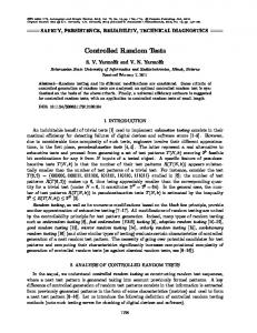
Fig. 2. Register file cell. The read current does not pass through the storage nodes, so the SNM is not impacted by reading the cell. The storage node does not rise when this cell is read
(a) 1.2 1
N1 (V)
0.8 0.6 0.4
V(N2) rises during read
0.2 0 0
0.2
0.4
0.6
0.8
1
1.2
N2 (V) (b)
Fig. 1. Conventional 6-T SRAM cell (a) and simulated SNM during a read operation, which is clearly attenuated in (b)
that manipulate the cell VSS have also been proposed [8][9]. In [10] IZENER currents are reduced in SRAM cells by use of a steeper halo angle and longer channel length, which provides a less abrupt doping transition and hence, reduced fields at the drain/source to bulk interfaces. This keeps IZENER low enough so that it is not dominant while the SRAM IOFF and IGATE are reduced through RBB and supply voltage collapse. Since SRAMs often employ nonminimum channel lengths to improve matching and reduce leakage currents, there is no area penalty for the longer channel length. In contrast, logic circuits can use other methods to retain state, i.e., thick-gate shadow latches [11]. It has been suggested that in sub-90 nm IC manufacturing processes and particularly those that are aggressively targeted, the efficacy of RBB may be decreased [12]. Again, since SRAMs often use less aggressive transistor lengths, this analysis may not apply to them. Additionally, IGATE may comprise a very significant percentage of the total transistor leakage. Only reduced voltage biases appear effective at mitigating increased IGATE due to transistor oxide scaling, at least until high-k gate dielectrics become common. C. SRAM read stability The current through the series transistors in the conventional 6-transistor (6-T) SRAM cell (see Fig. 1(a)) reduces the static noise margin (SNM) during a read. For example, if node N2 is at logic “0” and the WL is asserted high, the read current is passed through © 2008 ACADEMY PUBLISHER
transistors M5 and M1. M5 is saturated, but M1 is in the linear region of operation. Node N2 rises above VSS due to voltage division through the access and inverter pull down devices, i.e., between the pre-charged bit-line and the VSS terminal of the cell. This rise decreases the SNM during a read (see Fig. 1b). The voltage rise in the N2 storage node is determined by the cell ratio defined as the ratio of the gate width/length of the pull down transistors to that of the access transistors. The higher the cell ratio, the smaller the voltage drop across the pull down transistor and greater the SNM of the cell [13]. SRAM stability is usually ensured by appropriate transistor sizing to provide sufficient SNM during a read [13] but this is increasingly difficult for low-voltage designs. This has led to the use of level shifters and separate SRAM supplies to provide margin in SOC ICs that employ dynamic VDD scaling [14]. Transistors M1 and M3 must be stronger than M5 and M6, so that the logic low of the cell is not raised too high during read. Transistors M2 and M4 must however, be weaker than M5 and M6 to ensure write-ability, constraining the design space. Increasing mismatch due to lithographic and processing variations, including random dopant fluctuations (RDF) [15] and well proximity effects [16] has made SRAM stability problematic in modern highly scaled processes. The large number of cells per die enabled by Moore’s law requires consideration of statistics beyond six-sigma. Limiting lithographic mismatch has led to new SRAM cell layouts [17], further enabled by process features such as rectangular and unlanded contacts. These provide improved matching by analog design techniques, e.g., the use of rectangular diffusions and straight polysilicon runs. These geometries maintain transistor matching when the poly alignment to diffusion is imperfect. Such lithographically symmetrical cells improve SNM at low voltages, but do not improve random mismatch due to RDF. As VDD scales, the SNM reduces and in the presence of manufacturing variation, the SNM for a significant portion of the SRAM cells can vanish, significantly impacting IC yield. Register file (RF) cells decouple the read current path from the storage nodes, increasing SNM at the expense of area by using two additional transistors (see Fig. 2). In the RF cell shown in Fig. 2, transistors M7 and M8 provide a read current path that does not pass through the
JOURNAL OF COMPUTERS, VOL. 3, NO. 4, APRIL 2008
41
Fig. 3. Proposed 6-T LCSRAM cell with peripheral circuits, i.e., read and write WL and BL drivers, showing supplies
latch storage nodes. Consequently, the read current does not negatively affect the cell SNM.
in [20]. The read transistor, M6 is connected to the storage node through its gate as in an RF cell.
D. Paper organization This paper is organized as follows: Section 1 has provided a brief outline of the problems facing future SRAM designs, namely leakage mitigation and cell stability. In Section 2 a 6-T SRAM cell is described that intrinsically operates with reduced VDD when it is not being accessed and has improved read stability since it utilizes a single transistor read current path analogous to that of the 8-T RF cell. Basic memory design requirements and simulated operation are presented. Section 3 introduces 7-T SRAM cells which have better write margin than the 6-T cell. Two variations are examined, one of which has significantly better leakage mitigation characteristics. Section 4 presents results on more advanced CMOS processes to explore the leakage reduction and performance on future processes. Section 5 discusses static noise margin and process variation and shows the new cell has a good read stability over process variations. Section 6 gives measurement results of both 6T and 7-T cells on 130 nm process. Section 7 provides two methods to improve the read margin of 7-T cell. Section 8 concludes.
A. Read operation The 6-T LCSRAM cell supply voltage is raised from VCC = 0.3 V by the RWL driver during a read access, providing the full VDD power supply voltage to the cell (see Fig. 4). The RWL low voltage of VCC is apparent as the source voltage of the RWL driving inverter NMOS transistor in Fig. 3. The bit lines are pre-charged high by assertion of signal PCHN until a read or write operation. The energy required to move the supply of a cell row is similar to that in the drowsy memories mentioned above—here, the supply movement is integral to the read operation, but the energy required is similar. Moving the read path outside the cell storage nodes however, allows good read stability at much lower VDD. Depending on the cell state, i.e., logic “0” or logic “1”, the voltage on the gate of transistor M6 (node N1) in Fig. 3 is raised to VDD by the rising RWL voltage or maintained at VCC. In the former case, the BL (labeled BL_TOP in Fig. 3) is discharged low to VCC. The VCC bias at the source of transistor M6 isolates cells from one another. Biasing the source of M6 to VSS would allow sub-threshold conduction from non-accessed cells with VCC on node N1, i.e., a stored logic “1” at node N1, to participate in the discharge process. SRAM bit-line leakage is already a serious issue in modern CMOS fabrication technologies [21] which particularly impacts single-ended sense schemes such as the one used here. Cells storing a logic “0” at node N1 drive M6 with VGS = -VCC, greatly suppressing BL leakage, but without applying a high field that would increase IGATE through M6.
II. SIX-TRANSISTOR LEAKAGE-CONTROLLED SRAM The 6-T leakage controlled SRAM (LCSRAM) cell along with read and write circuits is shown in Fig. 3 [19]. Cell power is provided by the read word-line (RWL) signal as shown. When not accessed, the storage nodes have a reduced voltage labeled VCC (see Fig. 3) defined to be larger than the minimum data retention voltage DRVmin, e.g., 0.3 V, for the cells. The DRVmin is derived
© 2008 ACADEMY PUBLISHER
42
JOURNAL OF COMPUTERS, VOL. 3, NO. 4, APRIL 2008
1.25 CLK
0 1.25
WREN
V (V)
0 1.25
BL
0 1.25 WWL 0 1.25
VCC
0 1.25
RWL N1 N2
0 1.25
RD_OUT 0 1.8
2.44
3.08
3.72
4.36
5.0
Time (ns)
Fig. 4. 6-T LCSRAM write and read operation
The LCSRAM cell design in Fig. 3 uses a single BL for both read and write. This was chosen to optimize the layout area [19]. A single-ended sense is thus required. Sensing is accomplished with a high P to N ratio, i.e., skewed, static gate to provide the best speed. The complex CMOS gate provides an OR function of the bit lines above or below the sense and write circuits (see Fig. 3 where the BLs are labeled BL_TOP and BL_BOTTOM). Simulated write and read operation of a 32b x 128 LCSRAM sub-array at a clock speed of 700 MHz on the target foundry 0.13 µm process is shown in Fig. 4. Each BL has 64 cells attached to it. Higher performance can be supported by clocking at the local, rather than the global RWL, which adds two inversions to the timing critical path, or by shorter bit-lines. High speed single ended SRAM readout has been reported in [21]. Fig. 4 shows the RWL rise from the leakage controlled state (0.3 V) to the full voltage (1.2 V). The logic “1” LCSRAM cell internal storage node N1 rises with it. As a consequence, the BL discharges and the sense amplifier asserts the output RD_OUT high. The complimentary node, N2 remains low. The 6-T LCSRAM memory scheme does not require extra supply gating transistors to make the transition between active and drowsy mode—it is intrinsic to the operation so no additional control circuitry is required. No additional time is required to apply appropriate biases before reading and no additional energy is expended powering up un-selected rows or partial banks. Bias at VCC also applies back bias to the PMOS transistors of the unselected cells, further limiting their leakage. The scheme does require separate read and write BL drivers. B. Write operation Writing is single ended and is provided through transistor M5 (see Fig. 3). The data to be written is combined with the WRENN signal, which is the combination of write enable and clock. Asserting the write word line (WWL) high then begins the write to the storage node N1 as shown in Fig. 4. Since the cell is nominally operating in sub-threshold when not accessed, it is easy for a full voltage on the writing BL and WWL to overpower the cell voltage. However, the feedback transistors are operating in sub-threshold, resulting in a slow transition on complementary node N2. The cell write is accelerated by asserting RWL after the WWL
© 2008 ACADEMY PUBLISHER
Fig. 5. Butterfly curves showing conventional 6-T SRAM SNM cell and measured, non-degraded SNM of the LCSRAM when read
VCC
RWL
VSS
BL WWL
(a)
VDD
VCC
VSS
BL
VCC
RWL
WWL
(b)
Fig. 6. 6-T LCSRAM cell layout up to first level metal (M1) (a) and showing M2 and M3 only (b).
drives node N1 to the correct value, similar to the scheme proposed in [8]. Read operations require more time than write operation.. The delay between the WWL and the RWL signals is important to ensure writing the correct value to the cell. Using simulation, we have determined that a delay of 250 ps is adequate for all process corners, temperatures and VDD as low as 0.5 V on the target 130 nm process. The polarity of read and write are complementary when the BL is shared. This is easily handled by inverting the write logic. The BL is discharged when the RWL is asserted, removing the value to be written from the BL or alternatively, creating a contention state. Setting the BL high before writing, but not actively driving the BL during a write operation, alleviates the potential contention. Another complication of the LCSRAM is that the layout for the cells places adjacent cells from the same word next to each other instead of interleaved as in a conventional design. This is due to the separate WWL, and necessitates a hierarchical WL scheme to support a fine write granularity.
43
LBL
RBL
JOURNAL OF COMPUTERS, VOL. 3, NO. 4, APRIL 2008
Fig. 7. 7-T pwrt leakage controlled SRAM (LCSRAM) cell. 1.25
RWL
0 1.25 0 1.25
VCC VTP VCC
0 1.25
VDD -VTN
WWL
LBL RBL
V (V)
V (V)
0 1.25 0 1.25
0 1.25
VDD -VTNL
VCC
RBL
1.25
VCC
LBL 0 1.25
Fig. 9. 7-T nwrt leakage controlled SRAM cell.
VCC
0 1.25
VCC
0 1.25
N2 N1
VTPL
WWL
0 1.25
RWL
N1 N2
VCC
RD_OUT 0 0.8
1.5
2.2
2.9 Time (ns)
3.6
4.3
RD_OUT 5.0
Fig. 8. 7-T pwrt LCSRAM write and read operations.
C. 6-T LCSRAM read stability and BL slew rate SRAM SNM is often characterized by the “butterfly curve,” which consists of the inverter characteristics of the two SRAM storage nodes during a read operation. Local variation and mismatch cause the SNM curves to be asymmetrical. The diagonal of the maximum nested square measures the SNM [13]. As mentioned, in the proposed 6-T LCSRAM read current flow is decoupled from the storage node by the read transistor. Since the cell drives only the M6 gate, so there is no possibility of upsetting the storage nodes during the read operation. Fig. 5 shows the SNM measured on a fabricated cell with all nodes made probe-able. It is clear that the SNM of the 6-T LCSRAM is very good, essentially that obtained in flip-flops or other robust storage circuits. Since read path is through a single transistor, commensurately higher SRAM read currents might be expected. Unfortunately, the read current and hence BL slew rate (which impact read delay) are not greatly improved over that provided by the conventional SRAM cell, due to the RBB and reduced bias applied to M6 by the elevated source voltage. However, there is no restriction on the sizing of the read transistor M6. It can be made larger and consequently, a high read current can be obtained at a lower area penalty than in a conventional 6-T cell. D. 6-T LCSRAM physical design The cell layout uses 0.13 µm design rules. SRAM cells are generally designed using special, denser “array” design rules, which require close integration with the technology development and numerous fabrication runs
© 2008 ACADEMY PUBLISHER
0 4.0
8.0
12.0
16.0
20.0
24.0
Time (ns)
Fig. 10. 7-T nwrt LCSRAM write and read operations. Vwell = 2.0 V.
to verify manufacturability. Here, both the conventional and proposed 6-T SRAM are designed using the logic design rules. The symmetry of the conventional cell allows improved density, which is difficult to recover when the cell is not perfectly symmetric. Thus, the proposed 6-T LCSRAM design, which is non-symmetric, incurs an area cost. The cell layout is shown in Fig. 6(a), and is 11.3% larger than the conventional cell drawn to the same rules. The cell is wider than it is tall and all polysilicon gates are oriented in the horizontal direction. The metal routes are shown in Fig. 6(b) for clarity. VCC, RWL, and WWL are routed horizontally in M3. The BL is routed vertically in M2. VCC and VSS are also routed in M2. III. SEVEN-TRANSISTOR LCSRAM DESIGNS A. 7-T pwrt LCSRAM circuit and operation The write margin of the single ended 6-T LCSRAM is diminished from that of a conventional SRAM—it trades some write margin for improved read SNM. Fig. 7 illustrates a 7-transistor leakage controlled SRAM that has both improved read stability and write margin. The read transistor, M7 is in source follower configuration and there is no bit-line contention during write. The access transistors are PMOS to support this and require pre-discharged bit-lines prior to a write or a read. The cell is 11.5% larger than a conventional 6-T SRAM—nearly identical to that of the 6-T cell. The source-follower readout configuration provides improved leakage reduction over the 6-T LCSRAM. In the 7-T LCSRAM
44
JOURNAL OF COMPUTERS, VOL. 3, NO. 4, APRIL 2008
(a)
(b) Fig. 11. Monte Carlo simulations of SNM plots with five sigma variation in doping density and channel length at VDD=0.5V (a) 6-T LCSRAM (b) Conventional 6-T cell
design the polysilicon is oriented vertically. The cells are not rectangular, and vertically adjacent cells alternate the read BL connections [22]. The single-ended read is retained in the 7-T LCSRAM. While reading, the pre-discharged BL either rises from VCC towards VDD or remains at VCC depending on the data stored. In case of stored “1”, the BL rise is sensed and the output is latched. A simulated write followed by a read is shown in Fig. 8. The read transistor, M7 does not contribute to leakage due to the source-follower configuration. Consequently, a low Vt transistor can be used to improve the bit-line swing (shown by VDD – VTNL in Fig. 8) and the read delay. Writing is differential in this cell design. During a write access, one of the BLs is driven to VDD and the other is held at VCC. Writes are initiated by asserting the WWL signal low and accelerated by asserting RWL as before. There is no requirement to assert RWL as in the 6-T LCSRAM cell since there is write margin even in sub-threshold operation. B. 7-T nwrt LCSRAM circuit and operation Fig. 9 presents another 7-transistor SRAM cell variation. Again, this cell retains the full read SNM of the
© 2008 ACADEMY PUBLISHER
Fig. 12. Comparison of read SNM for conventional SRAM and LCSRAM at different supply voltages. Both mean value and five sigma value are given in the plot.
previous cell designs. Both NMOS and PMOS are reverse body biased in this cell to provide maximum leakage reduction. The RWL signal drives the NMOS sources instead of PMOS sources. PMOS RBB is provided by connecting N wells to a higher fixed supply voltage. NMOS RBB is applied by the cells’ raised NMOS source when unselected, i.e., when RWL is de-asserted high to VDD - DRVmin. The bit-line is pre-charged to VCC = 0.9 V and VDD = 1.2 V (DRVmin of 0.3 V is assumed here) prior to a read operation. The operation is shown in Fig. 10. The RWL signal is asserted low to VSS to initiate a read. A discharged bit-line is then sensed by the read out circuitry. To write this 7-T LCSRAM cell, one of the bitlines is discharged to VSS and the other is driven high to VCC as in a conventional SRAM cell. As before, the write is accelerated by the assertion of the RWL signal (see Fig. 10) but it is not required as in the 6-T LCSRAM. Applying RBB to both NMOS and PMOS transistors reduces the leakage by 52x over the conventional cell at VDD = 1.2 V. This is a considerable improvement over the previous two LCSRAM cell types that apply RBB to only the PMOS transistors. However, since back-bias is also applied to the PMOS source follower read transistor, read performance is diminished. The read transistor, M7 can again be low Vt to improve the speed (as shown by improved bit-line swing—see node VTPL in Fig. 10) without affecting the BL leakage currents substantially. IV. SLEW RATE AND LEAKAGE SIMULATION A. 6-T LCSRAM on 90 and 65 nm foundry processes The read speed (as measured by BL slew rate) and leakage suppression performance on foundry bulk 90 and 65 nm processes has been simulated. Transistor dimensions were scaled by 0.7x for each generation. The leakage currents at full VDD allow determination of the leakage power savings in the low power mode. The total leakage current of the 6-T LCSRAM cell in standby i.e., when RWL is driven to VCC, is reduced by 6.9x and 4.7x, respectively, on the 90 and 65 nm processes. VCC is 0.3 V for all cases, as the DRVmin is not expected to scale with
JOURNAL OF COMPUTERS, VOL. 3, NO. 4, APRIL 2008
45
0.80
0.90
1.00
0.80
0.90
1.00
0.70
0.60
0.50
0.40
0.30
1.5 1.45 1.4 1.35 1.3 1.25 1.2 1.15 1.1 1.05 1 0.95 0.9 0.85 0.8 0.75
(a)
0.70
0.60
0.50
0.40
1.5 1.45 1.4 1.35 1.3 1.25 1.2 1.15 1.1 1.05 1 0.95 0.9 0.85 0.8 0.75 0.30
Fig. 13. Chip micrograph with an overlay of one 0.5kB LCSRAM block.
(b) Fig. 14. Measured read access time from global WL enable to data out vs. VDD. VCC = 0.3 V in the measurements.
process or VDD. If the RBL is biased at VDD, i.e., they are left pre-charged in an always ready to read condition, the total cell leakage is dominated by leakage through the read transistor (M6 in Fig. 3). If the RBL is allowed to float, i.e., leak to VCC, the M6 leakage becomes negligible—this is the condition used in the simulations. In a large SRAM, this can be controlled by the bank select, given that there is sufficient time to precharge the BLs before a read. Since the cell is not symmetric, the leakage varies with the stored value. Consequently, the average values are shown. The PMOS RBB applied naturally by the scheme results in significant PMOS IOFF reduction, essentially eliminating this leakage component. The reduction is highly sensitive to the relative contributions of IGATE vs. IOFF as well as the relative leakages of NMOS vs. PMOS. On processes with very different PMOS vs. NMOS IOFF characteristics (such as that used in [19]) very high leakage reduction could be achieved. In most processes, NMOS IOFF has generally been dominant, to the point where PMOS RBB may not be applied [6]. The simulated BL slew rates with 64 cells per RBL give 1.78 V/ns for 90 nm and 1.48 V/ns for 65 nm process . These numbers
© 2008 ACADEMY PUBLISHER
Fig. 15. Shmoo plot of measured 6-T LCSRAM operation with VDD vs. VCC. Blanks indicate fails, while grey indicates full functionality. The read operation is shown in (a) and write operation in (b).
are comparable to those obtained with conventional SRAM cells. B. 6-T LCSRAM performance on a 45 nm double gate SOI process The 6-T cell is also simulated on a 45 nm double gate silicon on insulator (DG-SOI) process using the predictive technology models [23][24]. The 45 nm DGSOI transistors have essentially intrinsic channel doping, and hence low susceptibility to RDF. Additionally, the second, or back gate, can be used to change the apparent Vt of the controlling (or front) gate. The IOFF of the PMOS transistors on this technology is considerably lower than that of the NMOS transistors, similar to the technology used in [6]. Consequently, leakage control is only required for the NMOS transistors. The NMOS IDS leakage current (IOFF + IGATE) is 266 nA/Pm. Referring to Fig. 3, the storage pull down transistors M1, M3 and write transistor M5 require this back gate leakage control. The back gate of these transistors is driven to -1 V. Other transistors in the cell are connected so that both gates are controlling. The
46
JOURNAL OF COMPUTERS, VOL. 3, NO. 4, APRIL 2008
1E-10
VDD = 1.4V, 1.2V, 1.0 V, 0.8 V
Icc (A/cell)
1E-11
1E-12
1E-13 0.2
0.4
0.6
0.8
Vcc (V)
Fig. 16. Measured leakage current per LCSRAM cell at different VCC and VDD voltages. The BLs are connected to VDD in the measurements.
40 35
Power (uW)
30
40 MHz
25 20
20 MHz
15 10
10 MHz
5 0 0.95
1.05
1.15
1.25
1.35
VDD (V)
Fig. 17. Measured 6-T LCSRAM read power at different clock frequencies
leakage reduction provided with this configuration in the RWL = VCC = 0.3 V is 320x over the full RWL = VDD = 0.9 V condition. The SNM of the cell is improved by the reduced IDSAT of the back-gated NMOS transistors. The RWL to sense amplifier output delay is 54 ps. V. STATIC NOISE MARGIN AND PROCESS VARIATION The SRAM SNM is highly dependent on the transistor matching achieved. As process technologies move to the nanometer regime, the variation in CMOS transistor parameters, especially Vt increases drastically. The effect is particularly evident in minimum sized transistors as used in SRAMs to achieve the best possible density. In Fig. 11 Monte Carlo simulations run with sufficient trials to determine 5ı statistics for both the conventional 6-T SRAM and the proposed 6-T LCSRAM cell are shown. The 130 nm process variation parameters as supplied by the foundry are used, with VDD = 0.5 V. The simulations model Vt variation due to RDF and well proximity effects, as well as the variations in channel length and width. Local across-chip line width variation parameters are used. The envelope of SNM for both cells are shown as the grey area in Fig. 11. The 5 V worst-case
© 2008 ACADEMY PUBLISHER
for each cell is shown in the bold black lines. The same Monte Carlo simulations were run for different supply voltages starting from 1.2 V, which is the nominal VDD, down to 0.3 V, which is the minimum voltage we have assumed here can statically retain SRAM data. For a conventional 6-T SRAM cell, the read SNM is limited to approximately 100 mV even at VDD = 1.2 V. At VDD = 0.5 V, it has a nearly vanishing read SNM (see Fig. 11(b)). Only the 6-T LCSRAM cell is results are shown here, but the SNM is essentially the same for all configurations. Fig. 12 compares the read SNM of the conventional SRAM cell and LCSRAM at different supply voltages. The LCSRAM has a larger SNM than the conventional 6-T cell at every supply bias. Since the supply collapse is key to not only the low leakage in the LCSRAM designs, but also the read function, a fair comparison is between the SNM of the LCSRAM at RWL = VCC, e.g., at VCC = 300 to 400 mV, and the conventional SRAM at VDD = 1.2 V. The LCSRAM, with the transistor widths chosen here, has similar noise margin to the conventional SRAM in this comparison. Different P/N ratios can increase this value. Additionally, VDD cannot be very aggressively reduced for the conventional SRAM, while it can be when using the LCSRAM approach. This is important for ICs intended for low power, handheld devices, which now frequently employ dynamic VDD scaling to optimize power dissipation. VI. MEASURED RESULTS Three test SRAMs have been fabricated on two different 130 nm foundry fabrication runs, one SRAM array for each of the LCSRAM cell designs described. A. 7-T LCSRAM The LCSRAM test chip implementation uses hierarchical word lines. The global word line, combined with the sub bank select signal, activates the desired sub bank. Each sub-bank has a local WL decoder at the center of the sub-bank memory arrays. The test chip photomicrograph and the basic global decoder, local decoder and sub-bank blocks are shown in Fig. 13. The 130 nm memory array test chip has 64 LCSRAM cells per BL. Read and write accesses are 32 bits wide. The read access delay at 27oC vs. VDD comprises Fig. 14. The read path includes the global and local WL drivers, BL discharge, and sense circuit delays. The measured delay from global WL enable is 1.75 ns at 1.2 V and 572 ps at 1.7 V supply voltage. Faster access times are possible by clocking the sub-banks locally—the WLEN here is at the global WL. 6-T LCSRAM operation depends both on the supply voltage, VDD and on the storage voltage, VCC. The shmoo plot in Fig. 15 shows the usable VDD and corresponding VCC range for read and write operations. The read operation is functional at VDD as low as 0.78 V at 27oC with the corresponding VCC. At high VCC and low VDD the read operations fail due to the input logic threshold of
JOURNAL OF COMPUTERS, VOL. 3, NO. 4, APRIL 2008
47
1.30
1.20
1.10
1.00
0.90
0.80
0.70
0.60
0.50
0.40
0.30
0.20
0.10
1.5 1.4 1.3 1.2 1.1 1 0.9 0.8 0.7 0.6 0.5
(a) 1.5 1.4 1.3 1.2 1.1 1 0.9
Fig. 20. DC transfer curves of the highly low-skewd sense inverter with different NMOS source connections. The sense amplifier DC transfer characteristics with different VCC are shown. The BL swing for three VCC values is also shown as the shaded regions.
1.30
1.20
1.10
1.00
0.90
0.80
0.70
0.60
0.50
0.40
0.30
0.20
0.10
0.8 0.7 0.6 0.5
(b)
B. 7-T LCSRAM
Fig. 18. Measured 7-T pwrt LCSRAM read operation with VDD vs VCC.
1.30
1.20
1.10
1.00
0.90
0.80
0.70
0.60
0.50
0.40
0.30
0.20
1.5 1.4 1.3 1.2 1.1 1 0.9 0.8 0.7 0.6 0.5 0.10
operation power at three different clock frequencies. In these measurements, the BLs are pre-charged to VDD. Simulations indicate that floating the BL’s in inactive sub-banks reduces ISB substantially [22]. This capability was not provided in the test circuits.
(a) 1.5 1.4 1.3 1.2 1.1 1 0.9 0.8 0.7 0.6 0.5
Another 0.13 Pm test die similar to that shown in Fig. 13 utilizes the two 7-T LCSRAM cells described above. Fig. 18 shows the read and write operation shmoo plot of the 7-T pwrt LCSRAM test array. This cell can read and write at as low as 0.5 V at 27oC. The read operating region is narrow due to the narrow usable input range of the single-ended sense amplifier used in the test array and the low BL swing provided (see Fig. 8). Methods to widen single-ended sense amplifier input range are given in Section VII. The write operation region is much wider than that of the 6-T LCSRAM cell as expected. Write failures are only due to the data retention voltages. The shmoo plot for the 7-T nwrt LCSRAM comprises Fig. 19. This array can read at VDD as low as 0.5 V and can write at VDD as low as 0.58 V. High VCC failures during read are attributed to DRVmin violations. The same narrow single-ended sense range as the 7-T pwrt cell is the cause of the narrow read range for this cell as well. The write margin is the same as a conventional 6-T SRAM in this cell, as expected.
1.30
1.20
1.10
1.00
0.90
0.80
0.70
0.60
0.50
0.40
0.30
0.20
0.10
VII. 7-T LCSRAM WITH IMPROVED READOUT
(b) Fig. 19. Measured 7-T nwrt LCSRAM read operation with VDD vs VCC.
the single-ended sense amplifier. The write operation shmoo is similar but the single-ended write is clearly limiting. Fig. 16 illustrates the measured standby leakage power at different VDD. Fig. 17 shows the same measured © 2008 ACADEMY PUBLISHER
The read transistor (M7 in Fig. 7) in the 7-T pwrt LCSRAM is in source follower configuration and thus doesn’t contribute to the leakage power component. However, this also changes the read scheme. Instead of pre-charging the BL and discharging it through the read transistor as in both the conventional SRAM and 6-T LCSRAM designs, 7-T pwrt LCSRAM cell predischarges the BL and charges it when a logic one is stored in the cell (see Fig. 8). The BL rises slowly from VCC and slews to VDD-VTN. A high N/P skew sense amplifier improves the read delay. But, as evident in the shmoo plots of Fig. 18(a) and 19(a) this also narrows the
48
JOURNAL OF COMPUTERS, VOL. 3, NO. 4, APRIL 2008
RWL
within the BL swing across the usable VCC and thus provides adequate sense margins. As the output range of the sense inverter is from VCC to VDD, a level shifter is required in the following stage to prevent any possible leakage and restore the full voltage swing.
`
VDD
BLL
M7 M4
M2
BLR
VDD
VCC M5
N2
N1
M6
M1
M3
WWL
Fig. 21. Modified 7-T pwrt LCSRAM cell with common source read transistor 1.25 RWL
VCC 0 1.25
N1
V (V)
N2 -0.25 1.25 BLR
0 1.25 RD_OUT 0 5.0
6.0
5.5
6.5
7.0
Time (ns)
Fig. 22. Simulated read “1” from 7-T pwrt common source readout LCSRAM cell.
read operationg region. At higher VCC biases, the sense amplifer is triggered without a rise in the BL due to the increased VGS (VCC-VSS) and strong drive ability of the NMOS in the low-skewed sense amplifier. This results in the “skinny” shmoo plot for read operations in Fig. 18. Two approaches can be used to improve the read sense margin of 7-T LCSRAM. A. Improved sense gate logic threshold Fig. 20 compares the voltage transfer curve (VTC) of the sense gate at different VCC. The left most VTC corresponds to that used in the 7-T pwrt cell test chip in which the source of NMOS is connected to VSS. The dashed VTC in Fig. 20 shows that a better choice of P/N skew in the sense gate can provide functionality across a wider range of VDD and VCC values. In [25] a static inverter with virtual ground is used as sense amplifier to achieve a better single-ended BL sensing margin. Here, the NMOS transistor source in the sense gate is connected to VCC. Therefore, VGS (in this case VCC-VCC) of the NMOS transistor is always zero unless there is a rise in the BL. The solid curves in Fig. 20 are the inverter transfer charateristics with VCC biases ranging from 0.3 V to 0.5 V. The grey bars mark the BL swing, i.e., from VCC to VDD-VtN, for each case. The dots show the logic threshold of the sensing gate. In the orginal design, the sense inverter logic threshold is less than the lower end of the BL swing when VCC exceeds 0.4 V. Connecting the sense inverter NMOS transistor source node to VCC moves the logic threshold to lie
© 2008 ACADEMY PUBLISHER
B. Common-source read transistor Another approach to fix the narrow read margin is to alter the read transistor topology back to the common source used in the original 6-T cell as shown in Fig. 21. The source of the read NMOS transistor (M7) is connected to the fixed stand by voltage VCC instread of RWL. In the read operation, the BLL and BLR are precharged, and BLR either discharges to VCC through the read transistor or remains at VDD depending on the logic value stored in the cell. A larger BL swing is obtained. Fig. 22 shows the read operation in this 7-T pwrt LCSRAM configuration on the 0.13 Pm process. The interleaved read BL connections are retained, as is the non-rectangular cell layout. Each BL has 32 read transistors attached to it for a total BL height of 64 cells. The read operation is very similar to that of 6-T LCSRAM cell (see Fig. 4) as the read transistor topology is the same. However, the 7-T cell sacrifices some read out delay due to increased BL loading for larger PMOS access transistors. By changing the corresponding nodes and transistor connections, the same methods can be applied to 7-T nwrt cell as well. VIII. CONCLUSIONS In this paper, novel 6-T and 7-T leakage-controlled SRAM cells that maintain full static noise margin when reading have been presented. All are powered directly by the read word lines—instead of gating the cell supplies using separate circuitry, they intrinsically reside in a low voltage, leakage-controlled mode when not being accessed.. Both the 6-T and 7-T LCSRAM cells are less than 13% larger than a conventional 6-T SRAM cell drawn to the same rules. The leakage control is limited by the application of reverse body bias to only the NMOS transistors in two of the designs, but application of RBB to all of the transistors allows a 57x improvement in the 7-T nwrt design. Many processes appear to have very different NMOS and PMOS IOFF (c.f., [6] and [26]). The LCSRAM cell designs may provide sufficient leakage reduction on such processes. Judicious use of a controlling second gate bias on double gate SOI transistors, combined with the LCSRAM topology, provides excellent leakage control. Monte Carlo simulations using the foundry supplied variation parameters has been used to show the LCSRAM vs. the conventional 6-T SRAM SNM. The limiting LCSRAM SNM is that while the cell is biased at low voltage. For the conventional cell the SNM during reads is the limiting case. The reduced voltage LCSRAM SNM has been shown to be similar to the conventional cell read SNM at full VDD. The LCSRAM allows improved VDD scaling of the surrounding circuits without affecting the SNM.
JOURNAL OF COMPUTERS, VOL. 3, NO. 4, APRIL 2008
Fabricated LCSRAM circuit measurements on three of the many possible schemes have been presented. While the read sense margins in the 7-T test chips are marginal, this characteristic is due to poor PMOS to NMOS width selection and is readily improved. Circuit changes to effect this improvement have also been described.
49
[18]
[19]
ACKNOWLEDGMENT
[20]
This work was funded by SRC under task 1398.001. Test chip fabrication support was provided by AFRL/VSSE in Albuquerque, NM.
[21]
REFERENCES
[22]
[1] International Technology Roadmap for Semiconductors, 2003. http://www.itrs.org [online]. [2] D. Frank et al., “Device Scaling Limits of Si MOSFET’s and Their Application Dependencies,” Proc. IEEE, 89, pp. 259-288, March, 2001. [3] H. Mizuno et al., “An 18ȝA standby current 1.8V, 200 MHz microprocessor with self-substrate-biased dataretention mode,” IEEE J. Solid-state Circ., 34,pp. 14921500, Nov., 1999. [4] L. Clark et al., “Standby Power Management for a 0.18µm Microprocessor,” ISLPED Proc., pp. 7-12, 2002. [5] L. Clark, M. Morrow, and W. Brown, “Reverse Body Bias and Supply Collapse for Low Effective Standby Power,” IEEE Trans. VLSI Sys., 12, pp. 947-956, Sept., 2004. [6] K. Osada et al., “16.7fA/cell tunnel-leakage-suppressed 16Mb SRAM for handling cosmic-ray-induced multierrors,” ISSCC Proc., pp. 302-303, 2003. [7] K. Flautner, et al., “Drowsy caches: Simple techniques for reducing leakage power,” Proc. ISCA, pp. 148-156, 2002. [8] H. Mizuno and T. Nagano, “Driving Source-Line Cell Architecture for Sub-1V High-Speed Low-Power Applications,” IEEE J. Solid-state Circ., 31, pp. 552-557, April, 1996. [9] K. Min, K. Kanda, and T. Sakurai, “Row-by-row dynamic source-line voltage control (RRDSV) scheme for two orders of magnitude leakage current reduction of sub-1VVDD SRAM’s,” ISLPED Proc., pp. 66-71, 2003. [10] S. Zhao, et al., “Transistor optimization for leakage power management in a 65 nm CMOS technology for wireless and mobile applications,” VLSI Symp. Tech. Dig., pp. 1415, 2004. [11] L. Clark, F. Ricci, and M. Biyani, “Low Standby Power State Storage for Sub-130-nm Technologies,” IEEE J. Solid-state Circ., 40, pp. 498-506, Feb., 2005. [12] A. Keshavarzi, et al., “Technology Scaling Behavior of Optimum Reverse Body Bias for Leakage Power Reduction in CMOS IC’s,” ISLPED Proc., pp. 252-254, 1999. [13] E. Seevinck, F. List, and J. Lohstroh, “Static-noise margin analysis of MOS SRAM cells,” IEEE J. Solid-state Circ., SC-22, pp. 748-754, Oct., 1987. [14] L. Clark, US Patent #6,650,589, 2003. [15] A. Bhavnagarwala, T. Xinghai, and J. Meindl, “The impact of intrinsic device fluctuations on CMOS SRAM cell stability,” IEEE J. Solid-state Circ., 36, pp. 658-665, April, 2001. [16] Y. Sheu, et al., “Modeling the well-edge proximity effect in highly scaled MOSFETs,” IEEE Trans. on Electron Devices, Vol. 53, 11, pp. 2792-2798, Nov., 2006. [17] K. Kim, et al., “A novel 6.4 ȝm2 full-CMOS SRAM cell with aspect ratio of 0.63 in a high-performance 0.25 ȝm-
© 2008 ACADEMY PUBLISHER
[23] [24]
[25]
[26]
generation CMOS technology,” VLSI Tech. Symp. Dig., pp. 68-69, 1998. E. Morifuji, et al, “Supply and Threshold-Voltage Trends for Scaled Logic and SRAM MOSFETS,” IEEE Trans. Electron Devices, 53, pp. 1427 - 1432, Jun., 2006. S. Badrudduza, G. Samson, and L. Clark, “LCSRAM: Static Random Access Memory Cells with High Stability and Low Standby Power,” Proc. Int. VLSI Conf., pp. 2007. H. Qin, et al., “SRAM Leakage Suppression by Minimizing Standby Supply Voltage,” Proc. ISQED, pp. 55-60, 2004. S. Hsu, et al., "A 4.5-GHz 130-nm 32-KB L0 cache with a leakage-tolerant self reverse-bias bitline scheme,” IEEE J. Solid-state Circ., 38, pp. 755-761, May, 2003. S. Badrudduza, G. Samson, and L. Clark, “Static Random Access Memory Cells with Intrinsic High Stability and Low Standby Power,” J. Low Power Electronics, 2, 3, pp. 412-424, Dec. 2006. http://www.eas.asu.edu/~ptm, [online]. Y. Cao, et al., "New paradigm of predictive MOSFET and interconnect modeling for early circuit design," Proc. CICC, pp. 201-204, 2000. T. Kim, J Liu, J. Keane and C. Kim, “A high-density subthreshold SRAM with data-independent bitline leakage and virtual ground replica scheme,” Proc. ISSCC. pp. 329331, 2007. B. Calhoun and A. Chandrakasan, “A 256kb sub-threshold SRAM in 65nm CMOS,” Proc. IEEE ISSCC, pp. 628-629, 2006.
Sayeed A. Badrudduza received the B.S. degree in Electrical and Electronic Engineering from Bangladesh University of Engineering and Technology in 2000 and M.S. degree in Electrical Engineering from Arizona State University in 2002. He completed the PhD. degree from ASU in 2007. He has interned with Intel Corp. in Chandler, AZ, and Austin, TX. He is presently with Freescale Semiconductor in New York. Ziyan Wang received the B.S. degree in electrical and informatics engineering from Beijing Forestry University, Beijing, China in 2005. Since 2005, he has been working towards the master’s degree at Arizona State University. Giby Samson received the B.Tech degree in electronics and communication engineering from Regional Engineering College, Calicut, India in 1999 and M.S degree in Electrical Engineering from Arizona State University (ASU), Tempe, Arizona in 2004. Since 2004, he has been pursuing the Ph.D degree at ASU. He has interned with the Circuit Research Labs at Intel Corp. in Portland OR. Lawrence T. Clark received the B.S. degree in computer science from Northern Arizona University, Flagstaff, in 1984, and the M.S. and Ph.D. degrees in electrical engineering from Arizona State University, Tempe, in 1987 and 1992, respectively. He has over 15 years of semiconductor industry experience at Intel and at VLSI Tech. Inc. from 1982 to 2003 in positions ranging from microprocessor and chipset design to compact modeling. He contributed to Pentium, Itanium, and XScale processor designs. Most recently, he was a Principal Engineer and Circuit Design Manager for the XScale Microprocessors. Prof. Clark joined the Department of Electrical Engineering at Arizona State University, Tempe, AZ in 2004. He has been awarded over 55 patents.