M. Janaki Rani et al / Indian Journal of Computer Science and Engineering (IJCSE)
LEAKAGE POWER OPTIMIZED SEQUENTIAL CIRCUITS FOR USE IN NANOSCALE VLSI SYSTEMS M. Janaki Rani Faculty, ECE Department, Dr. M. G. R University, Maduravoyal, Chennai-95, India Research Scholar, Sathyabama University, Chennai – 600119, India
[email protected]
Dr. S. Malarkkan Principal, Manakula Vinayagar Institute of Technology, Puducherry, India
[email protected] Abstract As the density and operating speed of CMOS VLSI chips increases, leakage power dissipation becomes more and more significant. Therefore it is necessary to reduce the leakage power of portable battery operated devices. This paper proposes three power reduction techniques such as transistor stacking, self-adjustable voltage level circuit and reverse body bias for use in sequential circuits like D flip-flops and shift register. This work analyses the power of three different implementations of D flip-flops using pass transistors, transmission gates and gate diffusion input gates. All the designs are simulated with and without the application of leakage reduction techniques and the readings are presented. Also two bit, four bit and eight bit shift registers are simulated with stack and reverse body bias leakage reduction techniques. The circuits are simulated with MOSFET models of level 54 using HSPICE in 65 nm process technology with a supply voltage of 1 volt. Simulation results show that the proposed pass transistor based D flip-flop circuit has the least leakage power dissipation. In the case of shift registers the combined stack and reverse body bias method gives minimum leakage power of 19.51nW, 32.16nW and 98.34nW for two bit, four bit and eight bit shift registers respectively. Keywords: Leakage power, pass transistors, process technology, stacking effect, transmission gates. 1. Introduction Increasing demand for mobile electronic devices such as cellular phones, laptop computers and personal digital assistants requires the use of power efficient VLSI circuits. To minimize the power consumption and to increase the battery life time, the supply voltage Vdd has been scaled down continuously. But the propagation delay Tpd of a circuit is inversely proportional to the square of the difference between the supply voltage Vdd and the threshold voltage Vt of the transistors. So scaling down the supply voltage, without scaling down the threshold voltage increases the propagation delay. However the threshold voltage scaling results in substantial increase of sub-threshold leakage current, which increases the leakage or static power dissipation of the VLSI circuits [1]. Leakage power dissipation is the power dissipated by the circuit when it is in sleep mode or standby mode. Leakage power is given by [2] Pleak = Ileak * Vdd (1) where Ileak is the leakage current that flows in a transistor when it is in off state. This power dominates dynamic power especially in deep submicron circuits and also in circuits that remains in idle mode for a long time such as cell phones. Therefore in this paper the focus is on the reduction of leakage power dissipation. The leakage current consists of various components, such as sub-threshold leakage, gate leakage, reverse-biased junction leakage, gate-induced drain leakage [3]. Among these, sub-threshold leakage and gate leakage are dominant. The sub-threshold leakage current of a MOS device can be modeled as follows [2]:
ISSN : 0976-5166
Isubth=I0 exp[(Vgs-Vt) / (n VT) ] [1- exp (-Vds/VT)]
(2)
And I0=eff Cox (W/L)VT2
(3)
Vol. 3 No. 1 Feb -Mar 2012
32
M. Janaki Rani et al / Indian Journal of Computer Science and Engineering (IJCSE)
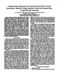
where eff is the electron/hole mobility, Cox is the gate capacitance per unit area, W and L are width and length of the channel respectively, Vt is the threshold voltage, n is the sub-threshold swing co-efficient, VT is the thermal voltage, Vgs is the transistor gate to source voltage and Vds is the drain to source voltage. This paper is organized as follows: Section 2 gives the related work in the area of flip-flop design. In section 3 we present three different designs of D flip-flops using pass transistors, transmission gates and Gate-Diffusion Input (GDI) gates. Section 4 describes three leakage reduction techniques such as transistor stacking, self-adjustable voltage level circuit and reverse body bias that are applied to the above designs. Section 5 presents the simulation results of the flip-flops and shift registers with and without the leakage reduction techniques and section 6 gives the conclusion. 2. Related Work In [4] Hamid et al. proposes a conventional data-retention scheme which uses a balloon latch applied to a transmission gate flip-flop. In this the balloon latch and some switches which are not in the critical paths use high threshold voltage transistors to reduce their leakage power. This scheme requires extra data-preserving balloon latches and complicated timing for transferring data back and forth between balloon latches and flipflops on any transition from power down to active mode and vice versa. In [5] David Levacq designed an ultra low power flip-flop using two ultra-low leakage diodes and analysis of master slave latches and flip-flops is discussed in [6]. In [7] Linfeng et al. proposes a new transmission gate flip-flop based on dual threshold CMOS technique to reduce it’s leakage power. In this low threshold transistors are assigned to critical paths of the circuits to enhance the performance, while high threshold transistors are assigned to non-critical paths to reduce the leakage current. In [8] Morgenstein et al. describes the implementation of D flip –flop using GDI gates. The analysis of single edge triggered flip flops is presented by D. Markovic et al. in [9] and Nedovic et al. in [10] describes the design of dual edge triggered flip-flops. Sagi Fisher et al. in [11] proposes two architectures for implementing flip-flop cells by integrating a GDI multiplexer in their design. 3. CMOS Implementation of D flip flops In this section three different implementations of D flip-flops in CMOS logic are presented. The D flip-flop combines a pair of master and slave D latch. Design – I uses pass transistors and inverters for the master-slave latches [12] as shown in figure 1. The two chained inverters are in memory state when the PMOS loop transistor is on, that is when clk = 0.Other two chain inverters on the right hand side acts in the opposite way. The flipflop changes its state during the falling edge of the clock. Figure 2 shows the design – II that uses transmission gates and inverters [12]. At the negative edge of the clock, transmission gates T1 and T4 are ON and transmission gates T2 and T3 are OFF. During this time the slave maintains a loop through two inverters P3, P4 and T4. Now the previous triggered value from Din is stored in the slave. At the same time master latches next state but as T3 is OFF it is not passed to slave. At the positive clock edge T2 and T3 are turned ON and the new latched value passes to slave through the loop of two inverters P1, P2 and T2. Figure 3 shows design –III with master-slave connection of two GDI D-latches [8]. In this the body gates are responsible for the state of the circuit. These gates are controlled by the clock (clk) signal and create two alternative paths. One for transparent state of the latch ,when the clk is low and the signals are propagating through PMOS transistors .The other one is for the holding state of the latch ,when the clk signal is high and internal values are maintained due to conduction of the NMOS transistors. The inverters are responsible for maintaining the complementary values of the internal signals and the circuit outputs.
ISSN : 0976-5166
Vol. 3 No. 1 Feb -Mar 2012
33
M. Janaki Rani et al / Indian Journal of Computer Science and Engineering (IJCSE)
Fig. 2. D flip-flop using transmission gates
Fig. 1. D flip-flop using pass transistors
Fig. 2. D flip-flop using transmission gates
Fig. 3. D flip-flop using GDI gates
4. Proposed Leakage Current Reduction Techniques In this section three leakage reduction techniques namely transistor stacking, self-adjustable voltage level circuit and reverse body bias that are applied to the above circuits are described. 4.1. Leakage current control using transistor stack The leakage current flowing through a stack of series connected transistors reduces when more than one transistor of the stack is turned OFF. This effect is known as the “Stacking Effect” [13]. When two or more transistors that are switched OFF are stacked on top of each other [refer figure 4(a)], then they dissipate less
ISSN : 0976-5166
Vol. 3 No. 1 Feb -Mar 2012
34
M. Janaki Rani et al / Indian Journal of Computer Science and Engineering (IJCSE)
leakage power than a single transistor that is turned OFF [refer figure 4(b)]. This is because each transistor in the stack induces a slight reverse bias between the gate and source of the transistor right below it, and this increases the threshold voltage of the bottom transistor making it more resistant to leakage. Therefore in figure 4(a) transistor T2 leaks less current than transistor T1 and T3 leaks less than T2. Hence the total leakage current through the transistors T, T2 andT3 is decreased as it flows from Vdd to Gnd. So Ileak1 is less than Ileak2. If natural stacking of transistors do not exist in a circuit, then to utilize the stacking effect a single transistor of width W is replaced by two transistors each of width W/2 [refer figure 4(c)].
(a)
(b)
(c)
Fig. 4. Transistor stacking effect
4.2. Self-adjustable voltage level circuit Figure 5 shows the general self-adjustable voltage level circuit [14], where Vdd is the supply voltage and VL is the output voltage of this circuit, which is applied to any load circuit. (In this paper D flip-flop is the load circuit). During the active mode (when SL=0), this circuit supplies maximum supply voltage to the load circuit through the ON PMOS transistor (P1) so that the load circuit can operate quickly. During the standby mode (SL=1), it provides slightly lower supply voltage to the load circuit through the weakly ON NMOS transistors (N1, N2, N3, ---Nm). So the voltage applied to the load circuit is given by VL = Vdd – Vn
(4)
where Vn is the voltage drop of m weakly ON NMOS transistors. The drain to source voltage Vdsn of the OFF NMOS in the standby mode is expressed as (5) Vdsn = VL - Vss = VL Vdsn can be decreased by increasing Vn that is increasing m, the number of NMOS transistors. When Vdsn is decreased, the drain- induced – barrier-lowering (DIBL) effect is decreased and this in turn increases the threshold voltage Vtn of NMOS transistors. Consequently the sub- threshold leakage current of the OFF MOSFETs decreases, so leakage power is minimized, while data are retained.
Fig. 5. D flip-flop with self-adjustable voltage level (SAL) circuit
ISSN : 0976-5166
Vol. 3 No. 1 Feb -Mar 2012
35
M. Janaki Rani et al / Indian Journal of Computer Science and Engineering (IJCSE)
4.3. Reverse body bias (RBB) This is an effective approach to reduce leakage power. In this method, when the circuit enters the standby mode, RBB is applied to increase the threshold voltage Vt of the transistors and this decreases the sub-threshold leakage current. Vt is related to the reverse bias voltage between the source and body Vsb by the following equation [15]: Vt = Vto + { (
)–(
)}
(6)
where Vto is the zero bias Vt for Vsb = 0volt, f is a physical parameter and is a fabrication-process parameter. Modification of Vt can be achieved by changing |Vsb| .This method can be either applied at the full chip level or a finer granularity. The advantage of this method is that it can be implemented without incurring any delay penalty. The key issue is that the range of threshold adjustment is limited, which in turn limits the amount of leakage reduction. 5. Simulation Results and Discussion In this work three designs of D flip-flops have been implemented in 65 nm CMOS process technology. The leakage power dissipation of the above circuits are compared with and without the power reduction techniques. The net lists of the circuits are extracted and simulated with BSIM4 models of MOSFET [16]. The simulations are done in HSPICE with a supply voltage of 1 volt, at a temperature of 27º C with a load capacitance of 50fF. The figure 6 shows the input-output waveforms of D flip-flop. The simulation results of D flip-flop with and without transistor stacking technique is presented in table 1. In this the leakage power reduction is more (13.05%) in D flip-flop designed using transmission gates. Table 2 shows the leakage power reduction using SAL technique and the reduction is maximum (34.67%) in transmission gate based D flip-flop. The design of D flip flops using pass transistors gives the minimum leakage current and using this flip flop 2-bit, 4-bit and 8-bit shift registers are implemented. The leakage power of the shift registers are compared with and without the stack and reverse body bias reduction techniques. The simulation results are shown in table 3 and for the shift registers the combined effect of RBB and stack method gives the least leakage power. Figure 7 shows the percentage reduction of leakage power in flip flops and figure 8 shows the leakage power in shift registers. 6. Conclusion Low leakage power D flip-flop circuits are proposed in this work. The leakage power of three designs of D flipflops are analyzed in 65 nm process technology. The percentage reduction of leakage power is more with the proposed SAL technique. The design of D flip-flop using pass transistors with SAL technique gives the minimum leakage power. Therefore for low leakage power applications D flip flop design using pass transistors can be used. In the case of shift registers leakage reduction is more for the combined approach of stacking and RBB technique.
Fig. 6. Input –output waveforms of D FF
ISSN : 0976-5166
Vol. 3 No. 1 Feb -Mar 2012
36
M. Janaki Rani et al / Indian Journal of Computer Science and Engineering (IJCSE)
Table 1. Leakage power of D flip-flops with stacking. Pleak (nW)
D FF Circuit
% Reduction in Pleak
Without stack
With stack
Pass transistors
16.42
14.95
8.95
Transmission gates
29.65
25.78
13.05
25.74
23.06
10.41
GDI gates
Table 2. Leakage power of D flip-flops with SAL circuit. Pleak (nW) D FF Circuit
% Reduction in Pleak
Without SAL
With SAL
16.42
13.46
18.03
29.65
19.37
34.67
25.74
20.94
18.64
Pass transistors
Transmission gates GDI gates
Table 3. Leakage power of shift registers with leakage reduction techniques Pleak of shift register (nW) S.No.
Reduction Technique used
1
2-bit
4-bit
8-bit
Base Case
26.43
51.84
119.92
2
Stack
23.94
38.56
107.65
3
RBB
25.17
49.35
114.18
4
RBB + Stack
19.51
32.16
98.34
35 30 25 %Reduction in 20 Pleak 15
PT
10
GDI
TG
5 0 Stack
SAL Reduction technique
Fig. 7. % Leakage reduction in flip flops
ISSN : 0976-5166
Vol. 3 No. 1 Feb -Mar 2012
37
M. Janaki Rani et al / Indian Journal of Computer Science and Engineering (IJCSE)
120 100 80 Basecase
Pleak in nW 60
stack
40
RBB
20
RBB+Stack
0 2-Bit
4-Bit
8-Bit
Shift register
Fig. 8. Leakage power in shift registers
References [1] [2] [3] [4] [5] [6] [7] [8] [9] [10] [11] [12] [13] [14] [15] [16]
International Technology Roadmap for Semiconductors (2005) Available at: http://www.itrs.net/Links/2005ITRS/Design2005.pdf Borivoje Nikolic (2008): Design in the Power–Limited Scaling Regime, IEEE transactions on Electron Devices, Vol. 55, No. 1, pp. 71-83. Yongpan Liu, Robert P. Dick, Li Shang, and Huazhong (2007): Accurate Temperature Dependent Integrated Circuit Leakage Power Estimation is Easy, EDAA 2007. Hamid Mahmoodi-Meimand and Kaushik Roy (2004): Data-Retention Flip-Flops for Power-Down Applications, Proceedings of IEEE International Symposium on Circuits and Systems (ISCAS 2004) , pp.677-680. David Levacq, Vincent Dessard, and Denis Flandre (2005): Ultra-Low Power Flip-Flops for MTCMOS Circuits, IEEE 2005. Stojanovic .V and Oklobdzija V.G. , (1999): Comparitive Analysis of Master Slave Latches and Flip-Flops for High-performance and Low-Power systems, IEEE Journal of Solid State Circuits, vol. 34, no.4, pp. 536-548. Linfeng Li and Jianping Hu (2009): A Transmission Gate Flip-Flop Based on Dual-Threshold CMOS Techniques, IEEE 2009. Morgenstein A., Fish A. , Wagner I. (2004): A Efficient Implementation of D Flip- Flop Using the GDI Technique, ISCAS’04, pp.673-676. Markovic D., Nikolic B., and Brodersen R.W. (2001): Analysis and Design of Low Energy Flip-Flops, International Symposium on Low Power Electronics and Design Tech. Dig., pp.52-55. Nedovic N. and Oklobdzija V.G.. (2005): Dual Edge Triggered Storage Elements and Clocking Strategy for Low Power Systems, IEEE Transactions on VLSI Systems, Vol. 13, No. 5, pp. 577-590. Sagi Fisher, Adam Teman, Dmitry vaysman, Alexander Gertsman, Orly Yadid-Pecht, and Alexander Fish (2009): Ultra Low Power Sub-Threshold Flip- Flop design, IEEE 2009. Doshi N. A, Dhobale S. B, and Kakade S.R (2008): LFSR Counter Implementation in CMOS VLSI, World Academy of Science, Engineering and Technology. Johnson M.C., Somasekhar D., Chiou L.Y., and Roy (2002): Leakage Control with Efficient Use of Transistor Stacks in Single threshold CMOS, IEEE Trans. VLSI, vol. 10, no.1, pp. 1-5. Tadayoshi Enomoto, Yoshinori Oka, and Hiroaki Shikano (2003): A Self-Controllable Voltage Level (SVL) Circuit and its LowPower High-Speed CMOS Circuit Applications, IEEE Journal of Solid State Circuits, vol. 38, no.7, pp.1220-1226. Liang yu Loy, Weijia Zhang, Zhi-Hui Kong, Wang-Ling Goh and Kiat-seg-Yeo (2008) : Body-Boootstrapped Buffer Circuit for CMOS Static Power Reduction, IEEE 2008. http://www- device.eecs.Berkeley.edu/~ptm/mosfet.
ISSN : 0976-5166
Vol. 3 No. 1 Feb -Mar 2012
38